In this post I have explained the datasheet, specifications, pinout configurations and a few application circuit for the IC IRS2153 which is a half-bridge IC from Texas Instruments. The unique feature of this half bridge driver is that it does not have to depend on external logic sources for the operations, rather allows configuring its own oscillator through a simple RC network.
The IC IRS2153(1)D which is fundamentally a half-bridge mosfet driver chip can be actually used for a number of different interesting circuit applications such as boost converters, solar compact inverters, and if two of them are coupled can be even configured as a full bridge mosfet driver circuit. I have explained more about this interesting device.
Main Electrical Specifications
Before I have explained the potential applications of this chip, I have explained a few of its main features first:
- The chip is designed to withstand and operate with voltages as high as 600V DC (15.4 V Zener clamp on VCC).
- Consists of an internal built-in oscillator circuit with a 50% fixed duty cycle, while its frequency can be simply determined through two external R/C components (CT, RT programmable oscillator).
- Consists of a built-in high side driver network which allows a fail-proof conduction of the high-side mosfet (upper mosfet) with the required essential boot-strapped gate voltage.
- Allows an external shut-down feature to be enforced just by adding an additional transistor stage with the IC (Non-latched shutdown on CT pin (1/6th VCC). This feature can be very useful for applications where an automatic current or voltage regulation is crucial.
- The chip also includes a Micropower start-up feature which assures guaranteed initialization even under relatively minimal voltage and current conditions.
- An internal dead time feature ensures perfect separation between the outputs for fail proof operations.
- All the the pinouts are ESD protected internally for safeguarding the chip against static voltages during packaging and handling.
Basic Circuit Configuration of the IC

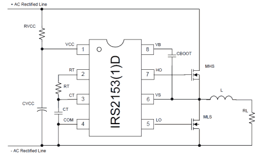
Understanding Pinouts of the Half-Bridge Driver IC IRS2153(1)D
The figure above shows the standard circuit configuration of the proposed half bridge IC. The pinout functions may be understood as follows:
Pin#1 is the Vcc of the IC and is internally clamped to 15.4V for safeguarding the IC from high supply voltages.
The RC network made from RVCC and CVCC has two important functions, the resistor hleps to control the current to the internal zener while the capacitor provides a start up delay to the chip so that the outputs are able to initiate with zero logic until the built-in oscillator has begun oscillating.
The resistor Rt and Ct across pin#2,3,4 is the external RC network which determine the oscillator frequency (duty cycle being fixed to 50% internally).
The following formula can be used for determining the oscillator frequency:
f = 1/1.453× Rt x Ct
Pin#4 is the ground terminal of the IC.
Pin#7 and pin#5 are the High and Low side outputs of the IC, meaning pin#7 drives the mosfet which is connected with the supply voltage while pin#5 is responsible for driving the mosfet connected with the ground rail.
Pin#8 is terminated with a Cboot capacitor which ensures that the HO and LO never conduct together and also steps-up the required bootstrapped voltage for the HO pinout of the IC.
Application Note:
The main application of this IC hovers around inverters and converter topologies.
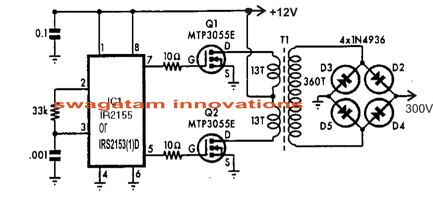
One standard inverter application design can be seen in the below given diagram:

The simple inverter design shown above using the IC IRS2153 can be used for driving mains CFL lamps from 12V supplies.
Here the Cboot feature is eliminated because the configuration is an ordinary center tap type inverter which does not call for boot-strapped supply due to the absence of high side mosfet network here.
The transformer may be wound over any standard 27mm E-core type ferrite assembly, as shown below.
For the complete datasheet you may refer to the following post:
irf.com/product-info/datasheets/data/irs2153d.pdf