In this post I have explained how to make a high current boost converter circuit which will step up a 12 V DC to any higher level up to 30 V maximum, and at an impressive 3 amp current rate. This high current output can be further enhanced by suitably upgrading the inductor wire gauge specifications.
Another great feature of this converter is that the output can be linearly varied through a potentiometer, from the minimum possible range to the maximum range.
Indroduction
DC -DC converters intended for stepping up car battery voltage are often configured around a switched mode type of power supply (SMPSU) or a power multivibrator, driving a transformer.
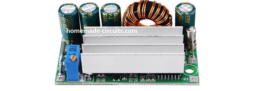
The 12V to 30 V power converter I have explained in this article employs the device TL 497A integrated circuit from Texas Instruments. This particular IC facilitates excellent voltage regulation with minimal output noise to be accomplished pretty conveniently, and likewise ensures high conversion performance.
How the Circuit Works
The high current converter circuit detailed here uses a flyback topology. The flyback theory appears to be the most suitable and functional technique of getting an immediate output voltage originating from a lower direct input voltage.
The main switching component in this boost converter circuit is actually a power SIPMOS transistor T1 (see Fig. 1). During its conduction period, the current passing through L1 increases exponentially with time.
During the ON time of the switching cycle, the inductor stores the induced magnetic energy.
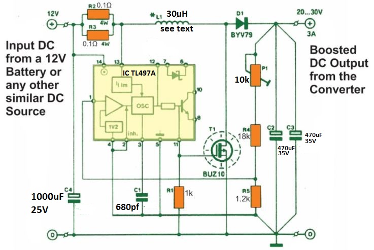
As soon as the transistor is switched off, the inductor reverts the stored magnetic energy, converting it into an electric current across the connected load via D1.
During this procedure, it is crucial to ensure that the transistor continues to be switched OFF for the period while the magnetic field on the inductor decays to zero.
In case this condition fails to implement, the current via the inductor soars up to the saturation level. An avalanche effect subsequently results in the current to maximize pretty quickly.
The relative transistor control trigger ON time, or duty factor thus, should not be allowed to get to the unity level. The maximum allowable duty factor relies, on various other aspects, around the output voltage.
This is because it decides the decaying rate of the magnetic field strength. The highest output power that could be achieved from the converter is determined by the highest allowable peak current processed by the inductor, and the switching frequency of the driving signal.
The restricting elements here are primarily the saturation instant and the inductor's maximum tolerable ratings for the copper losses, as well as the peak current via the switching transistor (do not forget that a spike of a specific electrical energy level comes to the output during each switching pulse).
Using IC TL497A for the PWM
The working of this IC is quite non-traditional, which could be understood from a short explanation below. Unlike the conventional fixed frequency implementation, variable duty factor SMPSU controller ICs, the TL497A is certified as a fixed on-time, adjustable frequency device.
Therefore the duty factor is controlled through adjustment in frequency to ensure a consistent output voltage.
This approach brings into reality a pretty straightforward circuit, nevertheless provides the downside of the switching frequency attaining to a lower range which may be audible to the human ear for loads working with lower current.
In reality, the switching frequency gets under 1 Hz once the load is removed from the converter. The slow clicks audible due to the charge pulses connected to the output capacitors to hold a fixed output voltage.
When there's no load attached, the output capacitors tend to get, obviously, gradually discharged through the voltage sensing resistor.
The internal oscillator on-time of IC TL497A is constant, and decided by C1. The oscillator could be deactivated in three methods:
- 1st, when the voltage on pin 1 increases beyond the reference voltage (1.2 V);
- 2nd, when the inductor current surpasses a specific highest value;
- And 3rd, by means of the inhibit input (although not utilized in this circuit).
While in standard working process, the internal oscillator allows the switching of T1 in such a way that the inductor current increases linearly.
When T1 is turned off, the magnetic energy accumulated inside the inductor is kicked back across the capacitor which are charged through this back emf energy.
The output voltage, along with pin 1 voltage of the IC TL497A, goes up slightly, which causes the oscillator to get deactivated. This continues until the output voltage has fallen to some significantly lower level This technique is executed in a cyclic manner, as far as theoretical assumption is concerned.
However, in an arrangement using actual components, the increase in voltage induced with the charging of the capacitors in a single oscillator interval is actually so tiny that the oscillator stays activated until the inductor current attains the highest value, as determined by the components R2 and R3 (the drop in voltage around R1 and R3 is usually 0.7 V at this point).
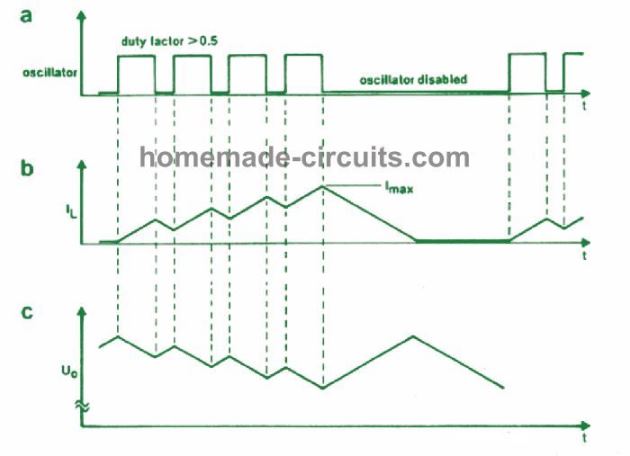
The step wise increase in the current as indicated in Fig. 2b is because of the oscillator signal duty factor which happens to be higher than 0.5.
As soon as the attained optimum current is reached, the oscillator gets deactivated, allowing the inductor to transfer its energy across the capacitors.
In this particular situation, the output voltage soars to a magnitude which is just high to ensure that the oscillator is switched OFF by means of IC pin 1. The output voltage now quickly falls, so that a fresh charge cycle is able to start and repeat the procedure.
However, sadly, the switching procedures discussed above will be combined with a comparatively large losses.
In a real life implementation, this issue can be remedied by setting up the on time (via C1) high enough to make sure that the current through the inductor never extends to the highest level in a single oscillator interval (see Fig. 3).
The remedy in such cases may be the incorporation of an air cored inductor, that features a reasonably minimal self-inductance.
Waveform Charateristics
The timing charts in Fig. 3 demonstrate signal waveforms on the key factors from the boost converter circuit. The main oscillator inside the TL497A works with a reduced frequency (below 1 Hz when the there's no load at te converter output).
The instantaneous time during switch-on, indicated as the rectangular pulse in Fig. 3a, depends upon the value of capacitor C1. The switch-off time is established by the load current. During the on-time switching, transistor T1 switches ON causing the inductor current to increase (Fig. 3b).
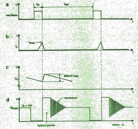
During the switch OFF period of time following the current pulse, the inductor works like a current source.
The TL497A analyzes the attenuated output voltage at pin 1 with its internal reference voltage of 1.2 V. In case the assessed voltage is lower than the reference voltage, T1 is biased harder so that the inductor adequately stores the energy.
This repeated charge and discharge cycles triggers a certain level of ripple voltage across the output capacitors (Fig. 3c). The feedback option allows adjusting of the oscillator frequency to ensure a the best possible compensation of voltage deficits caused by the load current.
The timing pulse diagram in Fig. 3d reveals substantial movement of the drain voltage because of the relatively high Q (quality) factor of the inductor.
Even though the stray ripple oscillations usually do not impact the regular functioning of this DC to DC power converter, these could be suppressed using a parallel 1 k resistor across the inductor.
Practical Considerations
Normally, an SMPS circuit is developed for achieving a maximum output current instead of quiescent output current.
High efficiency along with a steady output voltage together with minimum ripple are additionally become the key design objectives. On the whole, the load regulation features of a flyback based SMPS provide hardly any reason for concerns.
Throughout each switching cycle, the on/off ratio or the duty cycle is tweaked relative to the load current, in order that the output voltage continues to be relatively steady despite substantial load current fluctuations.
The scenario appears slightly different in terms of the general efficiency. A step-up converter based on the flyback topology typically produces fairly substantial current spikes, which may trigger significant loss of energy (do not forget that power increases exponentially as current increases).
In real life operation, however, the recommended high power boost solar converter circuit provides an overall efficiency better than 70% with optimum output current, and that looks pretty impressive with regards to the the simplicity of the layout.
This, consequently, demands it to get powered into saturation, leading to a reasonably extended turn-off time. Naturally, the more time it requires for the transistor to cut off the inductor current, the lesser will be the all round efficiency of the design.
In quite an unconventional manner, the MOSFET BUZ10 is switched through the pin 11 of the oscillator test output, instead of the internal output transistor.
Diode D1 is yet another crucial component inside the circuit. The necessities for this unit are an potential to endure high current spikes, and sluggish forward drop. The Type B5V79 fulfills all these requirements, and should not be substituted with some other variant.
Going back to the main circuit diagram of Fig. 1, it must be carefully noted that current highs of 15-20 A are generally not abnormal in the circuit. In order to avoid issues developing with batteries having a comparatively higher internal resistance, capacitor C4 is introduced like a buffer at the input of the converter.
Considering that the output capacitors are charged by the converter through quick, pulses like current spikes, a couple of capacitors are hooked up in parallel to make sure that run-a-way capacitance stays as minimal as it can be.
The high power DC converter actually does not feature not short-circuit protection. Short-circuiting the output terminals will be exactly like short circuiting the battery through D1 and L1. The self-inductance of L1 may not be not high enough to restrict the current for the period necessary to enable a fuse to blow.
Inductor Constructional Details
L1 is created by winding 33 and half turns of enameled copper wire. Figure 5 exhibits the proportions. The majority of companies provide enameled copper wire over an ABS roll, which usually works like the former for building the inductor.
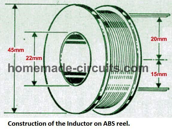
Drill a couple of 2 mm holes in the lower edge to slip the inductor wires. One of the holes will be near the cylinder while the other on the outer circumference of the former.
It may not be useful to consider thick wire to construct the inductor, due to the the skin-effect phenomenon, that causes the shift of charge carriers along the outer surface of the wire or the skin of the wire. This should be evaluated with regard to the magnitude of frequencies employed in the converter.
To guarantee a minimal resistance within the necessary inductance, it's advocated to work with a couple of wires of 1 mm diameter, or even 3 or 4 wires having 0.8 mm diameter in bunch.
About three 0.8 min wires will allow us to get a total dimension which may be approximately identical to two 1 mm wires, yet provides the an effective 20% higher surface area.
The inductor is tightly wound and could be sealed using an appropriate resin or epoxy based compound to control or suppress the audible noise leakage (remember that the frequency of operation is within the audible range).
Construction and alignment
The printed circuit board or the PCB design intended for the proposed high current 12 V to 30 V converter circuit is presented below.
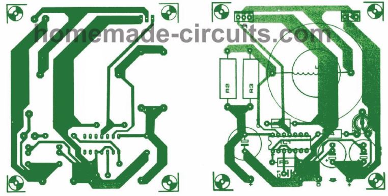
Several constructional factors needs to have some considerations. Resistors R2 and R3 might turn quite hot and therefore should be installed at the few mm elevated above the PCB surface.
The maximum current moving by means of these resistors could reach as large as 15 A.
The power-FET will also become substantially hot, and will demand a reasonably sized heatsink and the standard mica insulating kit.
The diode may possibly work without cooling down, though it may be ideally clamped over a common heatsink used for the power FET (do remember to insulate the devices electrically). While in usual functioning, the inductor may show fair amount of heating up.
Heavy-duty connectors and cables should be incorporated at the input and output of this converter. The battery is guarded with a 16 A delayed action fuse introduced within the input supply line.
Beware of the fact that the fuse will not provide any form of protection to the converter during output short circuits! The circuit is rather easy to set up, and may be done in the following manner:
Adjust R1 to achieve the intended output voltage which nay range between 20 and 30 V. The output voltage could be reduced below this, although must not be less than the input voltage.
This may be done by inserting a smaller resistor in place of R4. The highest output current can be expected to be approximately 3 A.
Parts List
| Component | Values/Details |
|---|---|
| Resistors (±5%) | |
| R1 | 1 kΩ |
| R2, R3 | 0.2 Ω; 4 W |
| R4 | 18 kΩ |
| R5 | 1.2 kΩ |
| P1 | 10 kΩ preset (H) |
| Capacitors | |
| C1 | 680 pF |
| C2, C3 | 470 µF; 35 V; radial |
| C4 | 1000 µF; 16 V; radial |
| Inductor | |
| L1 | 30 µH (home-made, see text) |
| Semiconductors | |
| D1 | BYV79 |
| T1 | BUZ10 or BUZ10A |
| IC1 | TL497A |
| Miscellaneous | |
| Heat-sink for T1 | |
| PCB Type 890030 |
Using IC SG3525 Boost Converter
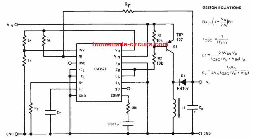
The popular IC SG3525 PWM IC could be used as high power DC 12 V to 30 V boost converter circuit application as shown above.
All the relevant circulations for determining the L1 coil details, the RF feedback resistor value and the output capacitor values are all furnished in the diagram itself.