We all are pretty familiar with the 78XX voltage regulator ICs or the adjustable types such as LM317, LM338 etc. Though these regulators are outstanding with their specified functioning and reliability, these regulators have one big disadvantage.... they won't control anything above 35V.
Circuit Operation
The circuit presented in the following article introduces a DC regulator design which effectively counters the above issue and is able handle voltages as high as 100V.
I am a great admirer of the above mentioned types of ICs simply because they are easy to understand easy to configure and require bare minimum number of components, and are also relatively cheap to build.
However in areas where input voltages can be higher than 35 or 40 volts, things become difficult with these ICs.
While designing a solar controller for panels which produces in excess of 40 volts, I searched a lot over the net for some circuit that would control the 40+ volts from the panel to the desired output levels, say to 14V, but was quite disappointed as I couldn't find a single circuit which could fulfill the required specifications.
All I could find was a 2N3055 regulator circuit which couldn't supply even 1 amp current.
Failing to find a suitable match I had to advise the customer to go for a panel that would not generate anything above 30 volts...that's the compromise the customer had to make using a LM338 charger regulator.
However after some thinking I could finally come up with a design which is able to tackle high input voltages (DC) and is a lot better than the LM338/LM317 counterparts.
Let's try to understand my design in details with the following points:
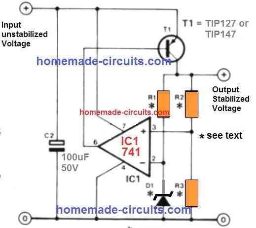
Referring to the circuit diagram, the IC 741 becomes the heart of the entire regulator circuit.
Basically it has been set up as a comparator.
Pin#2 is provided with t a fixed reference voltage, decided by the value of the zener diode.
Pin#3 is clamped with a potential divider network which is appropriately calculated for sensing the voltages exceeding the specified output limit of the circuit.
Initially when the power is switched ON, R1 triggers the power transistor which tries to transfer the voltage at its source (input voltage) across the other side of its drain pin.
The moment voltage hits the Rb/Rc network, it senses the rising voltage conditions and within a fraction of a second the situation triggers the IC whose output instantaneously goes high, switching off the power transistor.
This instantly tends to switch OFF the voltage at the output reducing the voltage across Rb/Rc, prompting the IC output to go low again, turning ON the power trasistor so that the cycle locks in and repeats, initiating an output level that's just exactly equal to the desired value set by the user.
Circuit Diagram

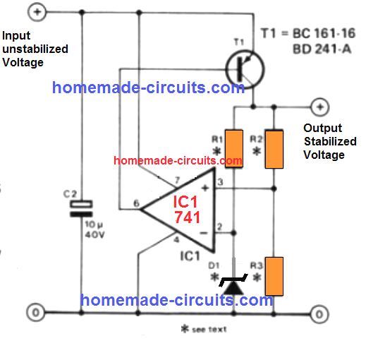
The values of the unspecified components in the circuit may be calculated by the following formulas and the desired output voltages may be fixed and set up:
R1 = 0.2 x R2 (k Ohms)
R2 = (Output V - D1 voltage) x 1k Ohm
R3 = D1 voltage x 1k Ohm.
The power transistor is a PNP, should be suitably selected which can handle the required high voltage, high current in order to regulate and convert the input source to desired levels.
You can also try replacing the power transistor with a P-channel MOSFET for even higher power output.
The maximum output voltage should not be set above 20 volts if a 741 IC is used. With 1/4 IC 324, the maximum output voltage can be exceeded up to 30 volts.
High Current Regulator with Low Dissipation
Power supply have been taken for granted since the introduction of the now-famous three-pin voltage regulators. However, there are times when such a regulator is insufficient. This sort of regulator requires a significant potential drop across it (usually greater than 3 V) and a high quiescent current (typically 6 mA for a 78xx). The regulator shown here is very appealing for battery-operated devices, as it provides:
- The output voltage is variable and highly steady.
- Reduced potential drop (some tenths of a volt).
- Quiescent current of a very small magnitude (20-30 uA).

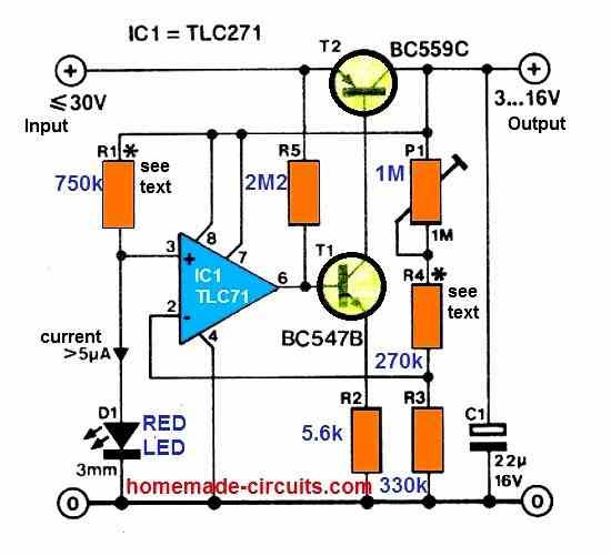
The regulator is a typical series type in theory. A common or garden red LED with a current demand of not less than 5uA is used as a voltage reference. An LED has a rather constant voltage drop at this modest current. The current is taken from the regulated output through R1. This improves the stability.
The TLC271 CMOS opamp provides regulation. By connecting pin 8 to the positive output terminal, this amplifier runs in the low bias mode, which assures extremely low current usage. The opamp's output is utilized as the basis drive for series regulator T2, which is driven by current source T1. This arrangement allows for good control of a tiny voltage swing at the opamp's output.
This is important because the opamp's slew rate in low-bias mode is rather low. The opamp gets its power from the regulator output as well. Capacitor C1 acts as a decoupling element for the opamp as a result. A type of bootstrap resistor, R5, was determined to be required for efficient control.
The settings of R1 and R4 in the diagram result in a 3 to 8 V adjustable output voltage. R4 can be increased by 200 k / V to get higher output voltages of up to 16 V. As long as the current through D1 does not decrease under 5uA, the value of resistor R1 must be raised as well.
Long connections in this sort of circuit should be avoided at all costs to avoid parasitic capacitances. The regulation would deteriorate as a result of this. The peak output current is primarily determined by the allowable dissipation in T2 and, to a minor extent, by the voltage difference between the input and output.
