This versatile Brushless (BLDC) motor controller IC is featured to control any desired high voltage, high current, hall effect sensor equipped 3-phase BLDC motor with extreme accuracy and safety. I have explained the details in depth.

Using the IC MC33035
The "hero" of the circuit is the single chip controller MC33035 which is a high performance second generation IC module, featuring all the required active functions that may be required to run most high current, high voltage, 3-phase or 4-phase BLDC motors with an open loop or a closed loop configuration.

The IC is equipped with a rotor position decoder for enabling an accurate commutation sequencing, temperature compensated reference for facilitating correct sensor voltage, a programmable frequency sawtooth oscillator, three in-built open collector high-side driver stages, and three high current totem-pole type low-side drivers, specifically designed to operate an 3-phase H-bridge high power mosfet motor controller stage.
The chip is also internally bolstered with high end protection features, and foolproof controls stages such as under-voltage lockout, cycle-by-cycle current limiting through an option of adjustable delay latched shutdown, internal IC high temperature shut down, and an exclusively devised fault output pinout which may be interfaced with an MCU for a preferred advanced processing and feed backs.
Typical functions that can be executed with this IC are, open loop speed control, forward reverse direction control, "run enable", an emergency dynamic brake feature.
The IC is designed to work with motor sensors having phases of 60 to 300 degrees or 120 to 240 degrees, as a bonus the IC can eb also used for controlling the traditional brushed motors.
How the IC Works
The MC33035 is amongst several high efficiency monolithic DC brushless motor controllers created by Motorola.
It's made up of just about the capabilities necessary to instigate a full−featured, open loop, three or four phase motor control system.
Furthermore, the controller can be accomplished to control DC brush motors. Designed with Bipolar Analog technology, it features a superior level of efficiency and durability in ruthless industrialized surroundings.
The MC33035 carries a rotor position decoder for accurate commutation sequencing, a environment reimbursed reference competent at delivering a sensor power, a frequency programmable sawtooth oscillator, a fully accessible error amplifier, a pulse width modulator comparator, 3 open collector top drive outputs, and 3 high current totem pole lower driver outputs just right for operating power MOSFETs.
Built into the MC33035 are shielding capabilities which includes undervoltage lockout, cycle−by−cycle current limiting with a selectable time delayed latched shutdown mode, in-built thermal shutdown, along with a exclusive fault output that will conveniently be interfaced to a microprocessor controller.
Standard motor control attributes incorporate open loop speed control, forward or reverse rotation, run enable, and dynamic braking. On top of that, the MC33035 has a 60°/120° select pin which configures the rotor situation decoder for either 60° or 120° sensor electrical phasing inputs.

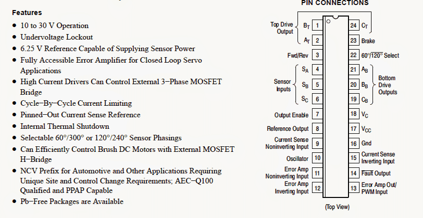
PIN OUT Functions:
Pin1, 2, 24 (Bt, At, Ct) = These are the three upper drive outputs of the IC specified to operate the externally configured power devices such as BJTs. These pinouts are internally configured as open collector mode.
Pin#3 (Fwd, Rev) = This pinout is intended to be used for controlling the direction of the motor rotation.
Pin#4, 5, 6 (Sa, Sb, Sc) = These are 3 sensor outputs of the IC assigned to command the control sequence of the motor.
Pin#7 (Output Enable) = This pin of the IC is assigned to enable the motor operation as long as a high logic is maintained here, while a low logic is for enabling a coasting of the motor.
Pin#8 ( Reference Output) = This pin is enabled with a supply current for charging the oscillator timing capacitor Ct as well as provide a reference level for the error amplifier. It can be also used for providing supply power to the motor Hall effect sensor ICs.
Pin#9 (Current Sense non-inverting Input): The signal output of 100mV may be achieved from this pinout with reference to pin#15 and is used for cancelling the output switch conduction during a specified oscillator cycle. This pinout normally links up with the upper side of the current sensing resistor.
Pin#10 (Oscillator): This pinout determines the oscillator frequency for the IC with the help of the RC network Rt, and Ct.
Pin#11 (Error amp non-inverting Input): This pinout is used with the speed control potentiometer.
Pin#12 (Error amp inverting Input): This pin is internally hooked up with the above mentioned error amp output for enabling the open loop applications.
Pin#13 (Error amp output/PWM Input): The function of this pinout is to provide compensation during closed loop applications.
Pin#14 (Fault Output): This fault indicator output may become an active logic low during a few critical conditions such as: Invalid Input code for the sensor, Enable pinout fed with a zero logic, Current sense input pinout getting higher than 100mV (@ pin9 with reference to pin15), triggering of the under voltage lockout, or a thermal shutdown situation).
Pin#15 (Current sense inverting input): This pin is set for providing the reference level for the internal 100mV threshold, and may be seen connected with the lower side current sense resistor.
Pin#16 (GND): This is the ground pin of the IC and is designated to provide the ground signal to the control circuit and is required to be referenced back to the power source ground.
Pin#17: (Vcc): This is the supply positive pin specified to the provide the positive voltage to the control circuit of the IC. The minimum range of operation of this pin being 10V and the max at 30V.
Pin#18 (Vc): This pinout sets the high state (Voh) for the lower drive outputs through the power attributed to this pin. The stage works with the range of 10 to 30V.
Pin#19, 20, 21 (Cb, Bb, Ab): These three pinouts are internally arranged in the form of totem pole outputs and are assigned to drive the lower drive output power devices.
Pin#22 (60 D, 120D phase shift select): The status attributed to this pinout configures the control circuit operation with the Hall effect sensors for either a 60 degrees (high logic) or 120 degrees (low logic) phase angle inputs.
Pin#23 (Brake): A logic low at this pinout will allow the BLDC motor to run smoothly while a logic high will instantly stop the motor operation through a rapid deceleration.
FUNCTIONAL DESCRIPTION
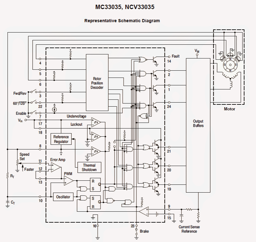
A representative internal block diagram is demonstrated in the above figure. A discourse of the benefits and working of each one of the central blocks enumerated below.
Rotor Position Decoder
An inner rotor position decoder meters the 3 sensor inputs (Pins 4, 5, 6) to render the the right sequencing of the upper and lower drive pinouts. The sensor inputs are manufactured to interface straight with open collector type Hall Effect switches or opto slotted couplers.
In-built pull−up resistors are classified to curtail the necessary amount of external parts. The inputs are TTL compatible, with their thresholds characteristically at 2.2 V.
The MC33035 range of ICs is intended to control 3 phase motors and run with 4 of the most popular conventions of sensor phasing. A 60°/120° Select (Pin 22) is expediently supplied and furnishes the MC33035 to configure on its own to regulate motors having either 60°, 120°, 240° or 300° electrical sensor phasing.
With 3 sensor inputs you will discover 8 potential input code formations, 6 of which are legitimate rotor placements.
The other two codes are outdated as they are generally a result of an open or shorted sensor connection.
With 6 justifiable input codes, the decoder may possibly take care of the motor rotor position to within a spectrum of 60 electrical degrees.
The Forward/Reverse input (Pin 3) is used as a tool to modify the course of motor schedule by reversing the voltage across the stator winding.
As soon as the input alters state, from high to low using a assigned sensor input program code (for instance 100), the facilitated top and base drive outputs using the same alpha status are swapped (AT to AB, BT to BB, CT to CB).
Essentially, the changeable string is changed direction and the motor reverses directional sequence. Motor on/off control is achieved by the Output Enable (Pin 7).
Whenever left disconnected, an internal 25 μA current supply permits sequencing of the leading and base drive outputs. When grounded, the top part drive outputs switch off and the base drives are pushed to low, evoking the motor to coast and the Fault output to trigger.
Dynamic motor braking makes it possible for a surplus margin of protection to be developed into the final device. Braking system is achieved by putting your Brake Input (Pin 23) within a higher status.
This leads to the top drive outputs to switch off and the underside drives to activate, shorting the motor−generated again EMF. The brake input possesses absolute, wholehearted consideration over all other inputs. The inner 40 kΩ pull−up resistor streeamlines interfacing using the program safety−switch by guaranteeing brake activation in case opened up or shut off.
The commutation logic truth table is shown in below. A 4 input NOR gate is employed to examine the brake input and the inputs to the 3 top drive output BJTs.

The objective is usually to turn off braking before the top drive outputs accomplish a high status. This allows you to avoid synchronized leasing of the the top and base power switches.
In half wave motor drive programs, the top drive components are generally not needed and they are in most cases kept detached. With these types of circumstances braking is still going to be attained because the NOR gate detects the base voltage to the top drive output BJTs.
Error-Amplifier
An improved efficiency, fully compensated error amplifier with active access to each inputs and output (Pins#11, 12, 13) is offered to assist in the execution of closed-loop-motor speed control.
The amplifier comes with a standard DC voltage gain of 80 dB, 0.6 MHz gain bandwidth, along with a wide input common mode voltage range that stretches from ground to Vref.
In the majority of open loop speed control programs, the amplifier is set up as a unity gain voltage follower with the noninverting input coupled to the speed set voltage supply.
Oscillator The frequency of the inner ramp oscillator is hard-wired through the values decided on for timing elements RT and CT.
Capacitor CT will be charged through the Reference Output (Pin 8) by means of resistor RT and discharged through an inner discharge transistor.
The ramp peak and pit voltages are normally 4.1 V and 1.5 V correspondingly. To offer a decent skimp on among audible noise and output switching performance, an oscillator frequency in the selection of 20 to 30 kHz is suggested. Make reference to Figure 1 for component selection.
Pulse Width Modulator
The integrated pulse-width-modulation offers an power effective approach to governing the motor speed by altering the standard voltage ascribed to every stator winding throughout the commutation series.
As CT discharges, the oscillator models each latches, enabling conduction of the uppper and lower drive outputs. The PWM comparator resets the top latch, terminating the lower drive output leasing once the positive−going ramp of CT turns into in excess of the error amplifier outcome.
The pulse-width-modulator timing diagram is demonstrated in Figure 21.
Pulse width modulation for speed management presents itself exclusively at the lower drive outputs. Current Limit Constant functioning of a motor that may be significantly over−loaded leads to overheating and inevitable malfunction.
This detrimental situation can easily best be averted together with the use of cycle−by−cycle current restriction.
That is, every on−cycle is dealt with as being a independent function. Cycle−by−cycle current restriction is achieved by tracking the stator current build−up everytime an output switch triggers, and after sensing a high current situation, instantly disabling the switch and retaining it off for the outstanding period of oscillator ramp−up interval.
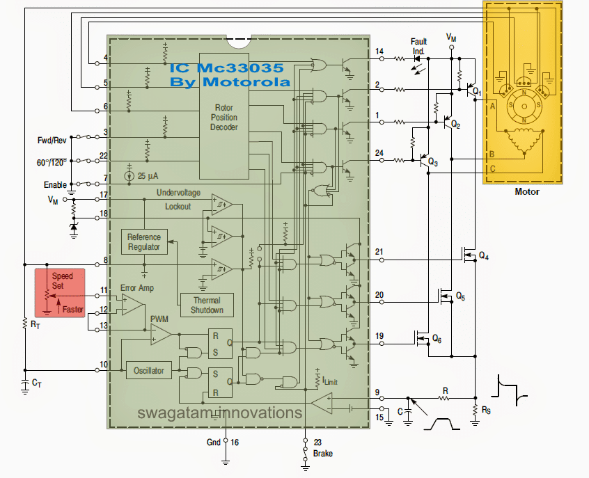
The stator current is transformed into a voltage through applying a ground−referenced sensing resistor RS (Figure 36) in line with the 3 lower part switch transistors (Q4, Q5, Q6).
The voltage established along the anticipating resistor is supervised with the Current Sense Input (Pins 9 and 15), and compared with the inner 100 mV reference point.
The current sense comparator inputs come with an input common mode range of roughly 3.0 V.
In the event the 100 mV current sense tolerance is surpassed, the comparator resets the lower sense lock and ends output switch conduction. The value for the current sensing resistor is actually:
Rs = 0.1/Istator(max)
The Fault output initiates while in an high amp situation. The dual−latch PWM setting makes certain that just one single output trigger pulse arises in the course of a certain oscillator routine, whether or not ended by way of the output of the error amplifier or the current limit comparator.
The on−chip 6.25 V regulator (Pin 8) offers charging current for the oscillator timing capacitor, a reference point for the error amplifier, which enable it to supply 20 mA of current appropriate for specifically powering sensors in low voltage programs.
In larger voltage purposes, this could grow to be important to exchange the power emitted from the regulator off the IC. This is definitely achieved with the help of another pass transistor as demonstrated in Figure 22.
A 6.25 V benchmark point seemed to be decided to enable rendering of the straightforward NPN circuit, wheresoever Vref − VBE surpasses the minimal voltage essential by Hall Effect sensors over heat.
Having proper transistor assortment and sufficient heatsinking, as much as 1 amp of load current can be purchased.
Undervoltage-Lockout
A three-way Undervoltage Lockout have been integrated to reduce harm to the IC and the alternative power switch transistors. During low power supply factors, it ensures the fact that IC and sensors are completely functional, and that there is adequate base drive output voltage.
The positive power supplies to the IC (VCC) and the low drives (VC) are each examined by independent comparators that get their thresholds at 9.1 V. This particular stage guarantees adequate gate commute required to attain low RDS(on) whenever driving ordinary power MOSFET equipment.
Whenever directly energizing the Hall sensors from the reference, inappropriate sensor operation appear in the event the reference point output voltage drops underneath 4.5 V.
A 3rd comparator can be used to recognize this issue.
When more than one of the comparators picks up an undervoltage situation, the Fault Output is turned on, the top runs are put off and the base drive outputs are organised in a low point out.
Each one of the comparators incorporate hysteresis to protect against amplitudes when bridging their individual thresholds.
Fault Output
The open collector Fault Output (Pin 14) had been intended to offer analysis details in case of a process breakdown. It has a sink current ability of 16 mA and may specifically drive a light emitting diode for visible signal. Furthermore, it is actually conveniently interfaced with TTL/CMOS logic for use in a microprocessor governed program.
The Fault Output is effective low while more than one of the subsequent situations take place:
1) Invalid Sensor Input codes
2) Output Enable at logic [0]
3) Current Sense Input more than 100 mV
4) Undervoltage Lockout, activation of 1 or higher of the comparators
5) Heat Shutdown, optimum junction temp getting maxed This exclusive output may also be used to tell apart between motor start−up or endured functioning within an inundated situation.
With the help of an RC network amongst the Fault Output and the enable input, this means you can develop a time−delayed latched shutdown with regard to overcurrent.
Additional circuitry displayed in Figure 23 helps make effortless starting up of motor systems that are fitted with higher inertial loads by giving supplemental pick-up torque, whilst still safe guarding overcurrent protection. This task is achieved by placing the current restrict to the next than minimal value for a established period. In the course of an exceedingly lengthy overcurrent situation, capacitor CDLY will charge, evoking the enable input to get across its tolerance to a low condition.
A latch can now be shaped by the positive feedback cycle from the Fault Output to the Output Enable. When set, by the Current Sense Input, it could only be reset by shorting CDLY or cycling the power supplies.
Fully Functional High Wattage BLDC Schematic
A Fully functional high wattage, high current BLDC controller circuit using the above explained device can eb witnessed below, it's configured as a full-wave, 3-phase, 6-step mode:

