The article below presents a comprehensive know how regarding how buck converters work.
As the name suggests, a buck converter is designed to oppose or restrict an input current causing an output that may be much lower than the supplied input.
In other words it can be considered a step down converter which could be used for acquiring calculated voltages or currents lower than the input voltage.
I have explained more regarding the working of buck converters in electronic circuits through the following discussion:

For a practical buck converter design you may want to read this article
The Buck Converter
Typically you may find a buck converter being used in SMPS and MPPT circuits which specifically require the output voltage to be reduced significantly than the input source power, without affecting or altering the power output, that is the V x I value.
The supply source to a buck converter could be from an AC outlet or from a DC power supply.
A buck converter is used only for those application where an electrical isolation may not be critically required across the input power source and the load, however for applications where the input may be at mains levels then a flyback topology is normally used through an isolating transformer.
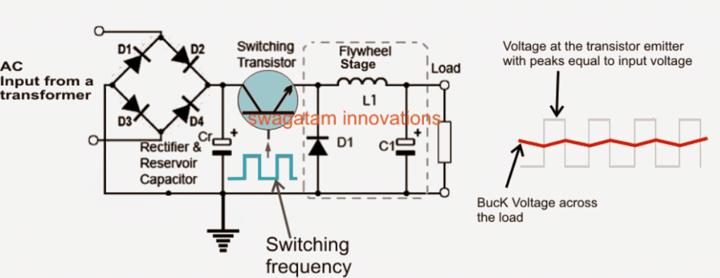
The main device which is used as the switching agent in a buck converter could be in the form of a mosfet or a power BJT (such as a 2N3055), which is configured to switch or oscillate at a rapid rate through an integrated oscillator stage with its base or gate.
The second important element in a buck converter is the inductor L, which stores the electricity from the transistor during its ON periods and releases it during its OFF periods maintaining a continuous supply to the load at the specified level.
This stage is also referred to as the "Flywheel" stage since its function resembles a mechanical flywheel which is able to sustain a continuous and steady rotation with the help of regular pushes from an external source.
Input AC or DC?
A buck converter is basically a DC to DC converter circuit that is designed to acquire a supply from a DC source, which may be a battery or a solar panel.
This could also be from an AC to DC adapter output achieved through a bridge rectifier and a filter capacitor.
No matter what may be the source of the input DC to the buck converter, it is invariably converted into a high frequency using a chopper oscillator circuit along with a PWM stage.
This frequency is then fed to the switching device for the required buck converter actions.
Buck Converter Operation
As discussed in the above section regarding how a buck converter works, and as may be seen the following diagram, the buck converter circuit includes a switching transistor and an associated Flywheel circuit which includes the diode D1, the inductor L1 and the capacitor C1.
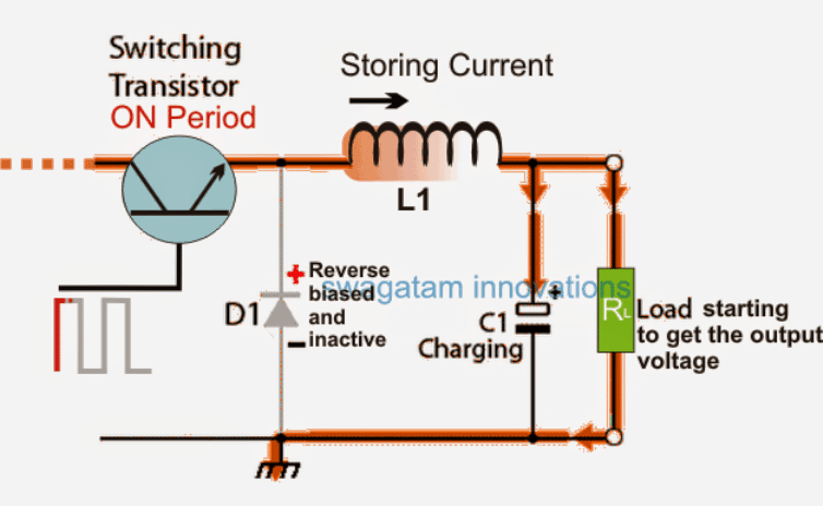
During the periods when the transistor is ON, the power passes first through the transistor and then through the inductor L1 and finally to the load. In the process, the inductor due to its inherent property tries to oppose the sudden introduction of current by storing the energy in it.
This opposition by L1 inhibits the current from the applied input to reach the load and reaching the peak value for the initial switching instants.
However in the meantime the transistor enters its switch OFF phase, cutting off the input supply to the inductor.
With the supply switched OFF L1 again faces a sudden change in the current, and to compensate the change it flushes out the stored energy across the connected load

Transistor Switch ‘on’ Period
Referring to the above figure, while the transistor is in the switch on phase, it allows the current to reach the load, but during the initial instants of the switch ON the current is heavily restricted due to the inductors opposition to the sudden application of the current through it.
However in the process the inductor responds and compensates the behavior by storing the current in it, and in the course some portion the supply is allowed to reach the load and also to the capacitor C1, which also stores the allowed portion of the supply in it.
It should also be taken into account that while the above happens, D1 cathode experiences a full positive potential which keeps it reverse biased, making it impossible for the L1's stored energy to get a return path across the load via the load. This situation allows the inductor to keep on storing the energy into it without any leakages.

Transistor Switch ‘off’ Period
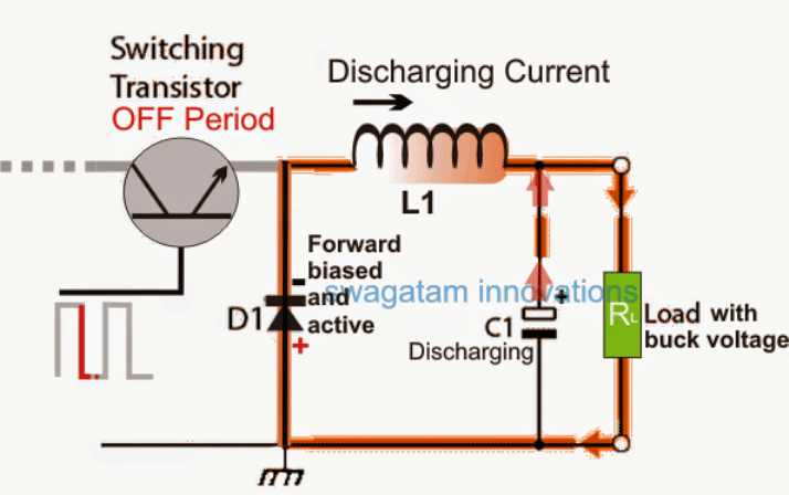
Now referring to the above figure, when the transistor reverts its switching action, that is as soon as it's turned OFF, the L1 is yet again introduced with a sudden void of current, to which it responds by releasing the stored energy towards the load in the form of an equivalent potential difference.
Now, since the T1 is switched OFF, the cathode of D1 is relieved from the positive potential and it's enabled with a forward based condition.
Due to the forward biased condition of D1, the released L1 energy or the back EMF kicked by the L1 is allowed to complete the cycle through the load, D1 and back to L1.
While the process is being completed the L1 energy goes through an exponential drop due to the load's consumption. C1 now comes to the rescue and assists or aids the L1 EMF by adding its own stored current to the load, thereby ensuring a reasonably stable instantaneous voltage to the load...until the transistor switches ON again to refresh the cycle back.
The whole procedure enables the execution of the desired buck converter application wherein only a calculated portion of the supply voltage and current is allowed for the load, instead of the relatively bigger peak voltage from the input source.
This may be seen in the form of a smaller ripple waveform instead of the huge square waves from the input source.
In the above section I have explained exactly how buck converters work, in the following discussion we'll delve deeper and learn the relevant formula of determining the various parameters related to buck converters.
Formula for Calculating the Buck Voltage in a Buck Converter Circuit
From the above decision we can conclude that the maximum stored current inside L1 depends on the ON time of the transistor, or the back EMF of L1 can be dimensioned by appropriately dimensioning the ON, and OFF time of L, it also implies that the output voltage in a buck converter can be predetermined by calculating the ON time of T1.
The formula for expressing the buck converter output may be witnessed in the below given relationship:
V(out) = {V(in) x t(ON)}/T
where V (in) is the source voltage, t(ON) is the ON time of the transistor,
and T is the "periodic time" or the period of one full cycle of the PWM, that is the time taken for completing one full ON time + one full OFF time.
Solved Example:
Let's try to understand the above formula with a solved example:
Let's assume a situation where a buck converter is operated with V(in) = 24V
T = 2ms + 2ms (ON time + OFF time)
t(ON) = 1ms
Substituting these in the above formula we get:
V(out) = 24 x 0.001/0.004 = 6V
Therefore V(out) = 6V
Now let's increase the transistor time by making t(ON) = 1.5ms
Therefore, V(out) = 24 x 0.0015/0.004 = 9V
From the above examples it becomes pretty clear that in a buck converter switching time t(ON) of the transistor governs the output voltage or the required Buck voltage, thus any value between 0 and V(in) could be achieved simply by appropriately dimensioning the ON time of the switching transistor.

Buck Converter for Negative Supplies
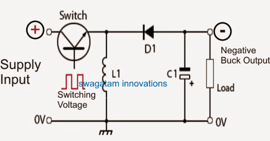
The buck converter circuit I have explained so far is designed to suit positive supply applications, since the output is able to generate a positive potential with reference to the input ground.
However for applications which might require a negative supply, the design could be slightly modified and made compatible with such applications.
The figure above shows that by simply swapping the positions of the inductor and the diode, the output from the buck converter may be inverted or made negative with respect to the available common ground input.