
In this post I will talk about the function of an interesting voltage regulator device: The LM337, which is basically the negative complementary device for the popular LM317 IC.
Built with an adjustable 3-terminal negative voltage, this regulator can conveniently supply around 1.5 A with an output voltage range of -1.2 V to -37 V.
It is incredibly easy to use and only needs two external resistors to configure the output voltage. Other cool features like internal current limiting, thermal shutdown and safe area compensation make the LM337 exceptionally robust.
This device caters to the various application including local and on-the-board voltage regulation. Further, the LM337 can be employed to construct a programmable output regulator. If you attach a permanent resistor between the adjustment and the output, the electronic component is transformed into a precision current regulator.
Being a complementary device for the IC LM317, which is a positive voltage regulator, the two are often used for making highly versatile dual voltage regulator power supplies.
Main Features
Some of the main features of the IC LM337 are:
- An additional 1.5 A output current
- Variable output voltage in the range of -1.2 V and -37 V.
- Built-in thermal overload guard
- Built-in short circuit, over current-limiting and over heat protection.
- Output transistor safe-area return
- An unrestricted operation for high-voltage applications
- Alleviates stocking of permanent voltages
- Available in surface mount D2PAK and typical 3-Lead transistor pack
- Lead-free and RoHS compliant
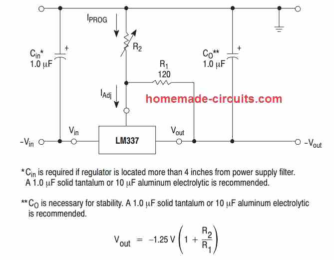
LM337 Variable Voltage Circuit Diagram
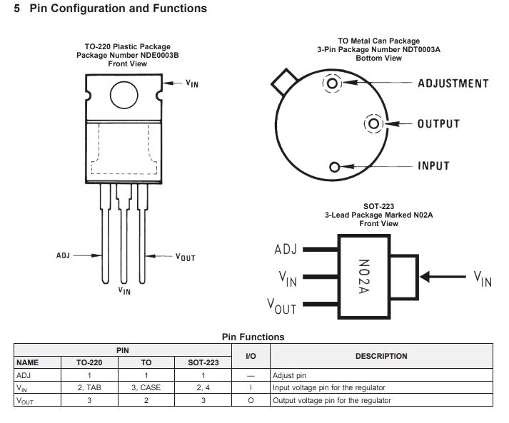
Pinout Details and Working
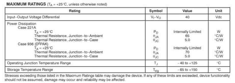
LM337 Absolute Maximum Rating
LM337 Electrical Characteristics
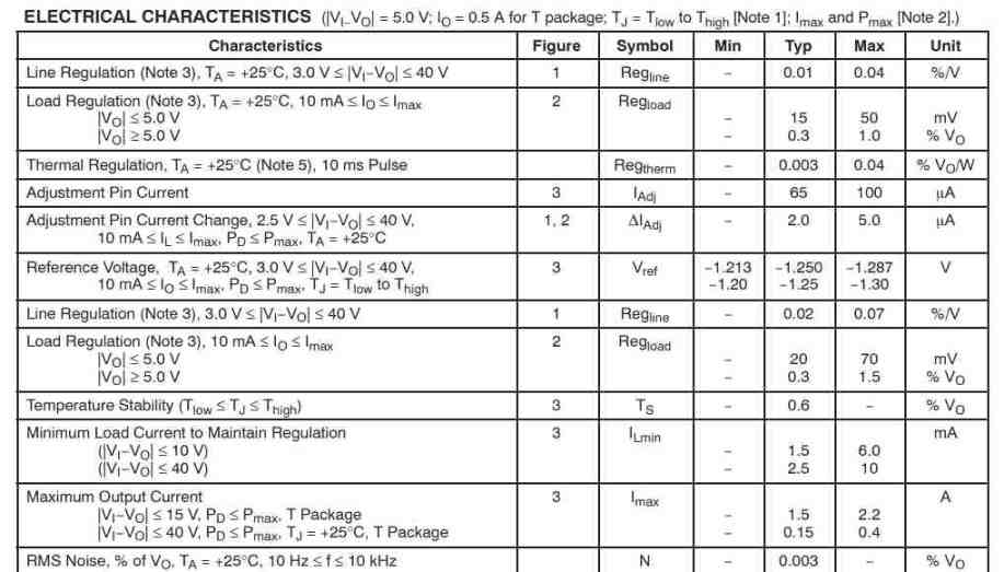
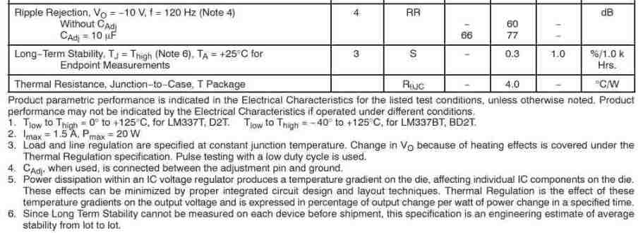
In the Electrical Characteristics for the listed test scenarios, the product parametric performance is shown, unless otherwise described.
There are a few exceptions where product performance may not be displayed in the Electrical Characteristics, as given below.
- Tlow to Thigh = 0° to 125°C, for LM337T, D2T. Tlow to Thigh = -40° to +125°C, for LM337BT, BD2T.
- Imax = 1.5 A, Pmax = 20 W
- The load and line regulation are noted at a constant junction temperature. There may be a change in VO due to the heating implications which is described under the Thermal Regulation specification. Here, a low duty cycle pulse testing is used.
- Cadj, if applied, is linked between the adjustment pin and ground.
- A temperature curve on the die is generated if there is power dissipation inside an IC voltage regulator. This affects the separate IC components on the die and its effects can be mitigated by good circuit design and layout methods. The effect of these temperature curves on the output voltage is given under Thermal Regulation, as the percentage of output change per watt of power change within a specified interval.
- Because Long Term Stability cannot be quantified on every component before shipment, this specification serves as a rough estimate of average stability.
Basic Circuit Operation and Working
The LM337 is a floating regulator with three terminals. It basically works by generating a precise -1.25 V reference (Vref) between its output and the regulation terminals.
This reference voltage is transformed to a programming current (IPROG) by R, as shown in Figure 17. As a result, this constant current travels via R2 from the ground.
The equation below describes the regulated output voltage:
Vout = Vref ( 1 + R2/R1) + IAdj R2
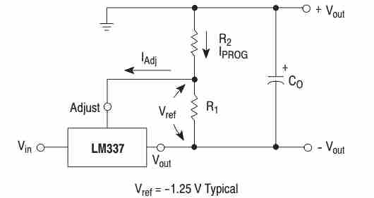
The LM337 can be used to regulate the adjustment terminal (IAdj) to lower than 100 µA and hold it constant, due to the fact that the current flowing into IAdj pin signifies an error term in the above formula. In order to implement this, all idle state operating current is sent back to the output terminal.
This forces the need for a minimum load current. As soon as the load current is at a lower level than this minimum, the output voltage will increase.
Moreover, because the LM337 works like a floating regulator, the most important characteristic that needs to perform is the voltage differential across the circuit. Additionally, it is also crucial that operation at high voltages relative to ground is achievable.
Load Regulation
The IC LM337 is versatile and will deliver an excellent load regulation, provided certain preventive measures are ensured for obtained best performance.
One example is that the programming resistor (R1) must be attached as near as possible to the regulator chip, to reduce line voltage drops which can easily join in series with the reference potential, seriously affecting the regulation efficiency.
The ground terminal of the R2 can be returned near the load ground to enable remote ground sensing and enhance load regulation.
External Capacitors
We recommend employing a 1.0 µF tantalum input bypass capacitor (Cin) to minimize the sensitivity to the input line impedance.
You can bypass the adjustment terminal to ground to enhance ripple rejection. This capacitor (Cadj) limits ripple from being boosted as the output voltage is adjusted towards higher levels.
Using a 10 µF capacitor can improve ripple rejection about 15 dB at 120 Hz when working with a 10 V application.
An output capacitance (CO) is supplied by a tantalum or 10 µF aluminium electrolytic capacitor is compulsory for stability.
Choosing either one of them with non-reduced ESR (Equivalent Series Resistance) value is also a must.
Low-ESR or capacitor rated with low ESR value and ceramic capacitors may lead to instability or permanent oscillations in the application.
Protection Diodes
If you are using external capacitors with any regulator IC, you might want to heavily consider including protection diodes to avoid the capacitors from discharging via low current points into the regulator.
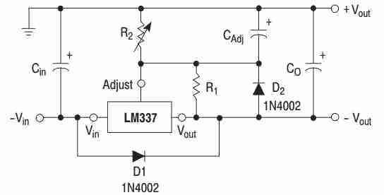
As shown in Figure above, the LM337 with some suggested protection diodes for output voltages more than -25 V or high capacitance values (CO > 25 µF, CAdj > 10 µF).
Diode D1 stops CO from discharging through the IC in the event of an input short circuit. Diode D2 safeguards capacitor CAdj discharging through the IC when an output short circuit occurs.
The combination of diodes D1 and D2 avoids CAdj from discharging via the IC if at all an input short circuit happens.
Reference: Datasheet