
IGBT stands for Insulated-gate-Bipolar-Transistor, a power semiconductor which includes the features of a MOSFET's high speed, voltage dependent gate switching, and the minimal ON resistance (low saturation voltage) properties of a BJT.
Figure 1 exhibits IGBT equivalent circuit, where a bipolar transistor works with a MOS gate architect, while the similar IGBT circuit is actually a mixture of a MOS transistor and a bipolar transistor.
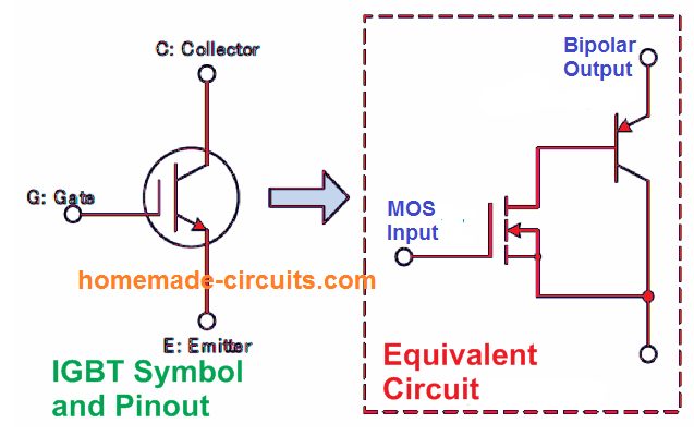
IGBTs, promising fast switching speed along with minimal saturation voltage characteristics, are being used in a extensive range, from commercial applications like in solar energy harnessing units and uninterruptible power supply (UPS), to consumer electronic fields, like temperature control for induction heater cooktops, air conditioning equipment PFC, inverters, and digital camera stroboscopes.
Figure 2 below reveals an evaluation between IGBT, bipolar transistor, and MOSFET internal layouts and attributes. The fundamental framework of the IGBT is same as that of a MOSFET having a p+ layer put into the drain (collector) section, and also an extra pn junction.
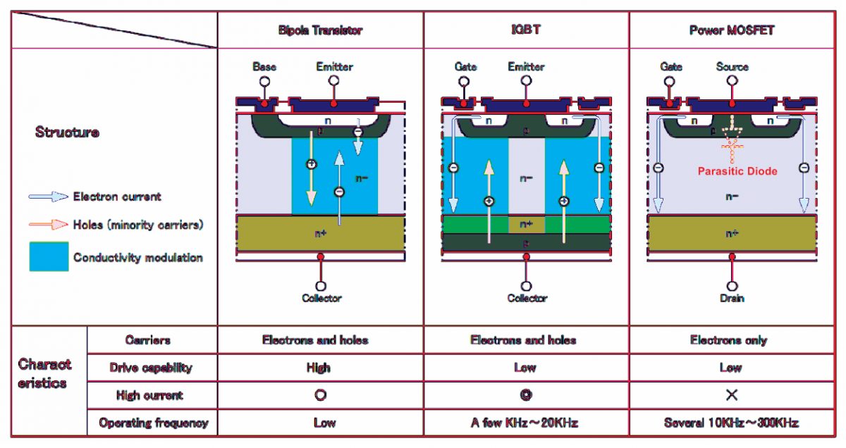
Due to this , whenever minority carriers (holes) tend to be inserted through the p+ layer on to the n- layer with conductivity modulation, the n- layer resistance gets reduced dramatically.
Consequently, the IGBT provides a reduced saturation voltage (smaller ON resistance) compared to a MOSFET when coping with huge current, thus enabling minimal conduction losses.
Having said that, considering that for the output flow path of holes, the accumulation of minority carriers at the turn-off periods, is prohibited due to the particular IGBT design.
This situation gives rise to a phenomenon known as tail current, wherein the turn-off is slowed down. When tail current develops, the switching period gets delayed and late, more than that of a MOSFET, resulting in an increase in the switching time losses, during the IGBT turn-off periods.
Absolute Maximum Ratings
Absolute maximum specifications are the values designated to guarantee safe and sound application of IGBT.
Crossing these specified absolute maximum values even momentarily may result in destruction or break down of the device, therefore please make sure to work with IGBTs inside the maximum tolerable ratings as suggested below.

Application Insights
Even if the recommended application parameters such as working temperature / current / voltage etc are maintained within the absolute maximum ratings, in case the IGBT is frequently subjected to excessive load (extreme temperature, large current/voltage supply, extreme temperature swings etc.), the durability of the device might get severely affected.
Electrical Characteristics
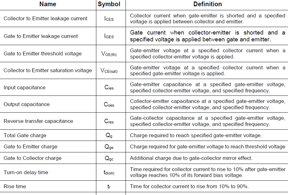
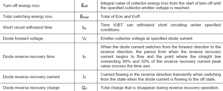
The following data informs us regarding the various terminologies and parameters involved with IGBT, which are normally used for explaining and understanding the working of an IGBT in detail.
Collector current, Collector Dissipation: Figure 3 demonstrates the collector dissipation temperature waveform of the IGBT RBN40H125S1FPQ. The maximum tolerable collector dissipation is displayed for various different case temperatures.
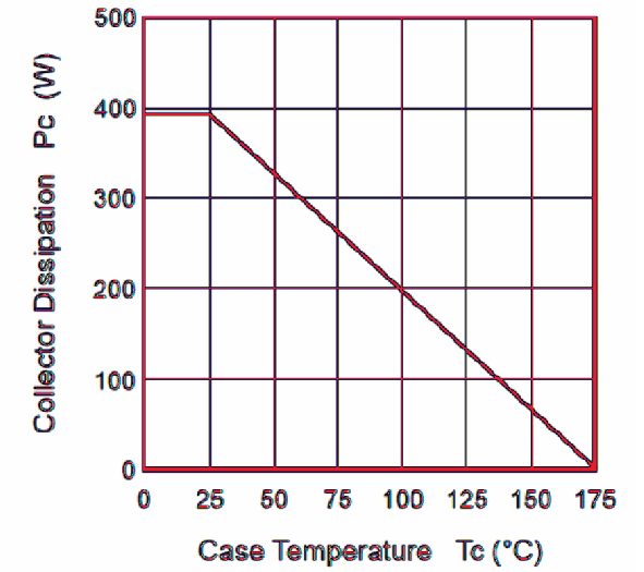
The below shown formula becomes applicable in situations when the ambient temperature TC = 25 degrees Celsius or more.
Pc = (Tjmax - Tc) / Rth(j - c)
For conditions where the ambient temperature TC is = 25℃ or lower, the IGBT collector dissipation is applied in accordance with their absolute maximum rating.
The formula for calculating the collector current of an IGBT is:
Ic = (Tjmax - Tc) / Rth(j − c)×VCE(sat)
However the above is the general formula, is simply a temperature dependent computation of the device.
Collector current of IGBTs is determined by their collector/emitter saturation voltage VCE(sat), and also depending on their current and temperature conditions.
Additionally, the collector current (peak) of an IGBT is defined by the amount of current it can handle which is in turn dependent on the way it is installed and its reliability.
For that reason, users are advised never to exceed the maximum tolerable limit of IGBTs while using them in a given circuit application.
On the other hand even if the collector current may be lower than the maximum rating of the device, it could get restricted by the unit's junction temperature or the safe operation area.
Therefore make sure you consider these scenarios while implementing an IGBT. Both the parameters, collector current and collector dissipation are usually designated as the maximum ratings of the device.
Safe Operating Area
The safe operating area (SOA) is dependent on the factors which ensure that the IGBT working condition (while being switched) is well inside the tolerable range of voltage, current and power magnitudes.
It is important to set up the layout of the circuit to ensure that the switching trajectory of the device during ON and OFF are always within the tolerable SOA (Figure 4).
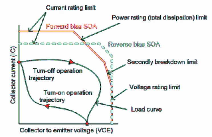
The SOA of an IGBT consists of a forward bias SOA and a reverse bias SOA, however since the particular range of values could differ in accordance with device specs, users are advised to verify the facts equivalent in the data sheet.
Forward Bias Safe Operating Area
Figure 5 illustrates the forward bias safe operation area (FBSOA) of the IGBT RBN50H65T1FPQ.
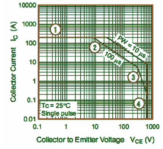
The SOA is split into 4 regions depending on particular limitations, as outlined below:
- Area restricted by the highest rated collector pulse current IC(peak).
- Area restricted by collector dissipation region
- Area restricted by the secondary breakdown. Remember that this kind of malfunction causes the safe operating area of an IGBT to get narrower, except when the device features a secondary breakdown margin.
- Area restricted by maximum collector to emitter voltage VCES rating.
Reverse Bias Safe Operating Area
Figure 6 demonstrates the reverse bias safe operation area (RBSOA) of the IGBT RBN50H65T1FPQ.
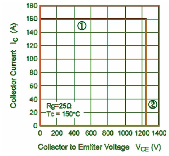
This particular characteristic works in accordance with the reverse bias SOA of the bipolar transistor.
Whenever a reverse bias, which includes no bias, is supplied across the gate and the emitter of the IGBT during its turn-off period for an inductive load, we find a high voltage being delivered to the IGBT’s collector-emitter.
Simultaneously, a large current constantly moves as a result of residual hole.
Having said that, in this functioning the forward bias SOA cannot be used, while the reverse bias SOA can be utilized.
The reverse bias SOA is divided into 2 restricted areas, as explained in the following points; eventually the area is established by validating the real functioning procedures of the IGBT.
- Area restricted by the maximum peak collector current Ic(peak).
- Area restricted by the maximum collector-emitter voltage breakdown rating VCES. Observe that the IGBT may get damaged if a specified VCEIC operation trajectory strays away from the device's SOA specifications.
Hence, while designing an IGBT based circuit, it must be ensured that the dissipation and other performance issues are as per the recommended boundaries, and also the specific characteristics and circuit breakdown constants relevant to breakdown tolerance must be taken care of.
For instance, reverse bias SOA carries a temperature characteristic which dips at extreme temperatures, and the VCE/IC operating locus shifts in accordance with the IGBT's gate resistance Rg and gate voltage VGE.
That is why, it is vital to determine the Rg and VGE parameters with respect to the working ecosystem and lowest gate resistance value during switch off periods.
In addition, a snubber circuit could be helpful for controlling the dv/dt VCE.
Static Characteristics
Figure 7 indicates the output characteristics of IGBT RBN40H125S1FPQ. The picture represents the collector-emitter voltage while the collector current passes within a random gate voltage situation.
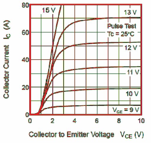
The collector-emitter voltage, that impacts the current handling efficiency and loss during switch ON condition, varies according to the gate voltage and body temperature.
All these parameters needs to be taken into account while designing an IGBT driver circuit.
The current goes up whenever VCE reaches the values of 0.7 to 0.8 V, although this is because of the forward voltage of the PN collector-emitter PN junction.
Figure 8 demonstrates the collector-emitter saturation voltage vs. gate voltage characteristics of IGBt RBN40H125S1FPQ.
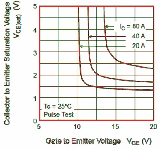
Essentially, VCE (sat) begins dropping as the gate-emitter voltage VGE rises, although the change is nominal while VGE = 15 V or higher. Therefore, it is advised working with a gate/emitter voltage VGE that's around 15 V, whenever possible.
Figure 9 exhibits the collector current vs. gate voltage characteristics of IGBT RBN40H125S1FPQ.
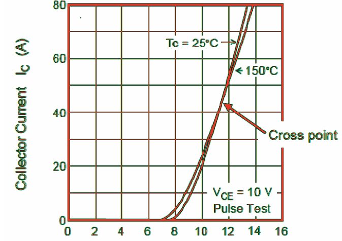
The IC/VGE characteristics are based on temperature changes, however the region of low gate voltage towards the intersection point, tend to be negative temperature coefficient, while the high gate voltage region signifies positive temperature coefficients.
Considering that power IGBTs will generate heat while in operation, it is actually more advantageous to pay attention to the positive temperature coefficient region particularly when the devices are operated in parallel.
The recommended gate voltage condition using VGE = 15V exhibits the positive temperature characteristics.
Figures 10 and 11 demonstrate how the performance of the collector-emitter saturation voltage, along with gate threshold voltage
of an IGBT are dependent on temperature.
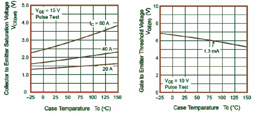
Due to the fact that the collector-emitter saturation voltage features a positive temperature coefficient characteristics, it is not easy for current to pass while the IGBT operation is dissipating high amount of temperature, which becomes responsible for blocking the effective current during parallel IGBT operation.
On the contrary, the operation of gate-emitter threshold voltage relies on negative temperature characteristics.
During high heat dissipation, the threshold voltage falls downward, causing a higher possibility of malfunctioning of the device resulting from noise generation.
Therefore, mindful testing, centered around the above specified characteristics may be crucial.
Gate Capacitance Characteristics
Charge Characteristics: Figure 12 demonstrates the gate charge characteristics of a stabdard IGBT device.
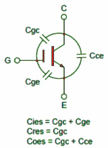
IGBT gate characteristics are essentially in line with the very same principles applied for power MOSFETs and provide as the variables that decide the device's drive current and drive dissipation.
Figure 13 reveals the characteristic curve, divided into Periods 1 to 3.
The working procedures related with each period are I have explained below.
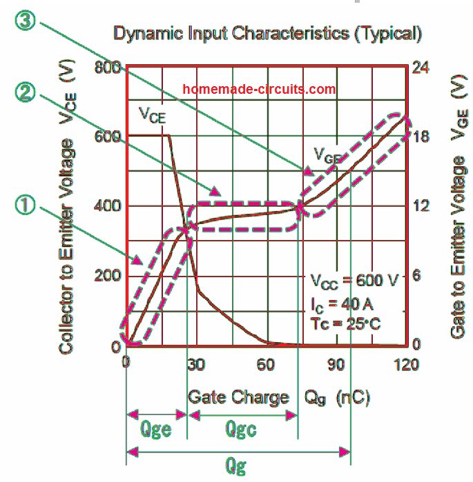
Period 1: Gate voltage is raised up to threshold voltage where current just starts to stream.
The section ascending from VGE = 0V is the portion responsible for charging the gate-emitter capacitance Cge.
Period 2: While the transition from the active region to the saturation region transpires, the collector-emitter voltage begins altering and gate-collector capacitance Cgc gets charged.
This particular period comes with a noticeable increase in capacitance because of the mirror effect, which causes VGE to become constant.
On the other hand while an IGBT is entirely in the ON state, the change in the voltage across collector-emitter (VCE) and the mirror effect vanish.
Period 3: In this particular period the IGBT gets into a completely saturated condition and the VCE shows no changes. Now, the gate-emitter voltage VGE begins increasing with time.
How to Determine Gate Drive Current
The IGBT gate drive current depends upon the internal gate series resistance Rg, signal source resistance Rs of the driver circuit, the rg element which is the internal resistance of the device, and the drive voltage VGE(ON).
The gate drive current is calculated using the following formula.
IG(peak) = VGE(on) / Rg + Rs + rg
Keeping the above in mind, the IGBT the driver output circuit should be created ensuring a current drive potential equivalent to, or bigger than IG(peak).
Typically, the peak current happens to be smaller than the value determined using formula, because of the delay involved in a driver circuit and also the delay in the dIG/dt rise of the gate current.
These may occur on account of aspects such as wiring inductance from the drive circuit to the gate connection point of the IGBT device.
Additionally, the switching properties for each turn-on and turn-off may be hugely dependent on Rg.
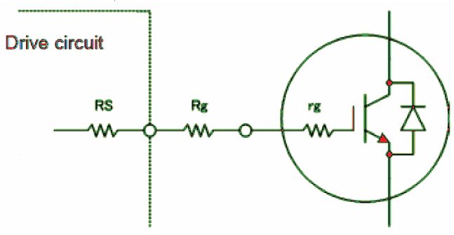
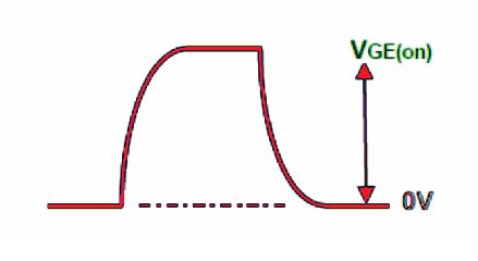
This eventually may be impacting switching time and switching deficits. It is crucial to choose a suitable Rg with respect to the device's characteristics in use.
Drive Loss Calculation
The losses occurring in IGBT driver circuit can be depicted through the below given formula if all of the losses developed from the driver circuit are absorbed by the above discussed resistance factors. (f indicates the switching frequency).
P(Drive Loss) = VGE(on) × Qg × f
Switching Characteristics
Considering that the IGBT is a switching component, its switch ON, switch OFF speed is among the main factors impacting its operating efficiency (loss).
Figure 16 demonstrates the circuit which can be used for measuring the Inductance Load switching of an IGBT.
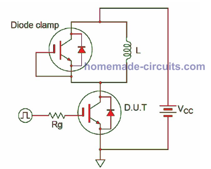
Because the diode clamp is hooked up in parallel to inductive load L, the delay of the IGBT turn-on (or the turn-on loss) is usually afflicted by the diode’s recovery time characteristics.
Switching Time
The Switching time of an IGBT, as displayed in Figure 17, can be categorized into 4 measurement periods.
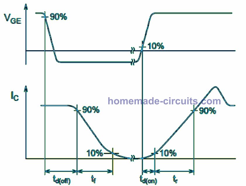
Due to the fact that the time changes drastically for every single period with respect to Tj, IC, VCE, VGE, and Rg situations, this period is assessed with the following outlined conditions.
- td(on) (turn-on delay time): The point of time from where the gate-emitter voltage extends to 10% of forward bias voltage to a level until the collector current increases to 10%.
- tr (rise time): The point of time from where the collector current increases from 10% to 90%.
- td(off) (turn-off delay time): The point of time from where gate-emitter voltage attains 90% of forward bias voltage to a level until the collector current drops to 90%.
- tf (fall time): The point of time from where the collector current reduces from 90% to 10%.
- ttail(tail time): The IGBT turn-off period consists of a tail time (ttail). This can be defined as the time consumed by the excess carriers leftover on the IGBT's collector side to recede through recombination despite of the IGBT getting shut off and causing the collector-emitter voltage to increase.
Built-in Diode Characteristics
In contrast to power MOSFETs, the IGBT doesn't involve a parasitic diode.
As a result, an integrated IGBT that comes with a pre-installed Fast Recovery Diode (FRD) chip is employed for inductance charge control in motors and identical applications.
In these types of equipment, the working efficiency of both the IGBT and the pre-installed diode significantly impacts the equipment working efficiency and noise interference generation.
Additionally, reverse recovery and forward voltage qualities are crucial parameters related to the in-built diode.
Built-in Diode Reverse Recovery Characteristics
The concentrated minority carriers are discharged during the switching state just when forward current passes via the diode until the reverse element state is attained.
The time needed for these minority carriers to be fully released is known as the reverse recovery time (trr).
The operational current involved throughout this time is termed as reverse recovery current (Irr), and the integral value of both of these intervals is known as the reverse recovery charge (Qrr).
Qrr = 1/2(Irr x trr)
Considering that the trr time period is equivalently short circuited, it involves a huge loss.
Additionally, it restricts the frequency throughout the switching process. On the whole, fast trr and reduced Irr (Qrris small) is deemed optimal.
These qualities are greatly dependent on the forward bias current IF, diF/dt, and junction temperature Tj of the IGBT.
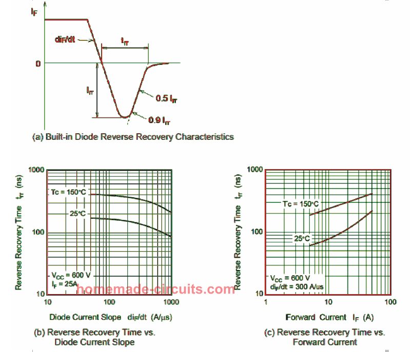
On the other hand, if trr gets faster, di/dt results in being steeper around the recovery period, as happens with the corresponding collector-emitter voltage dv/dt, which causes an increase in the propensity for noise generation.
Following are the examples which provides the ways through which noise generation can be countered.
- Decrease diF/dt (reduce IGBT switch-ON time).
- Include a snubber capacitor across the collector and emitter of the device to minimize collector-emitter voltage dv/dt.
- Replace the built-in diode with some soft recovery diode.
The reverse recovery property significantly relies on the voltage/current tolerance capacity of the device.
This feature could be enhanced using lifetime management, hefty metallic diffusion, and various other techniques.
Built-in Diode Forward Voltage Characteristics
Figure 19 exhibits the output characteristics of in-built diode of a standard IGBT.
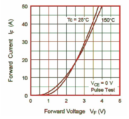
Diode forward voltage VF signifies declining voltage produced when current IF through the diode runs in the direction of the diode's forward voltage drop.
Since this characteristic may result in power loss in the course of back EMF generation (free-wheeling diode) in motor or inductive applications, selecting smaller VF is recommended.
Additionally, as depicted in Figure 19, the positive and negative temperature coefficient characteristics is determined by the diode's forward current magnitude IF.
Thermal Resistance Characteristics
Figure 20 depicts the resistance characteristics of the IGBT against thermal transients and integrated diode.
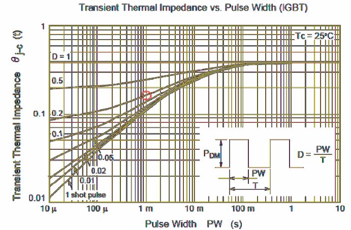
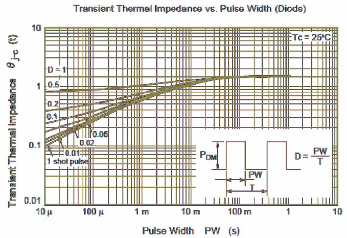
This characteristic is used for determining junction temperature Tj of the IGBT. The pulse width (PW) shown over the horizontal axis signifies the switching time, which defines the single one shot pulse and the results of repetitive operations.
For instance, PW = 1ms and D = 0.2 (duty cycle = 20%) signifies that the repetition frequency is 200Hz since the repetition period is T = 5ms.
If we imagine PW = 1ms and D = 0.2, and dissipation power Pd = 60W, it is possible to determine the increase in IGBT junction temperature ΔTj in the following manner:
ΔTj = Pd × θj - c(t) = 60 × 0.17 = 10.2
Load Short Circuit Characteristics
Applications that require bridged IGBT switching circuits like inverters, a short circuit (overcurrent) protection circuit becomes imperative for withstanding and protecting against damage during the time until the IGBT gate voltage is switched OFF, even in a situation of an output short circuit of the unit.
Figure 21 and 22 indicate the short circuit bearing time and short circuit current handling capacity of the IGBT RBN40H125S1FPQ.
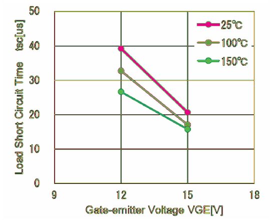
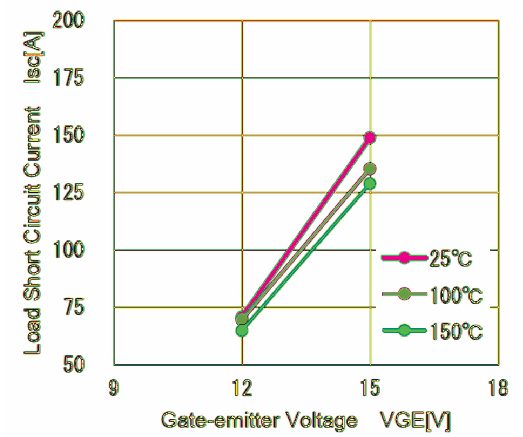
This short circuit withstanding capacity of an IGBT is commonly expressed with regard to time tSC.
This withstanding capability is determined mainly based on the IGBT's gate-emitter voltage, body temperature, and power supply voltage.
This ought to be looked at while designing a critical H-bridge IGBT circuit design.
Additionally make sure to opt for an optimally rated IGBT device in terms of the following parameters.
- Gate-emitter voltage VGE: With an increase in the gate voltage, the short circuit current also rises and the current handling capacity of the device decreases.
- Case temperature: With an increase in the case temperature ΔTj of the IGBT, the current withstanding capacity declines, until the device reaches the breaks down situation. Power supply voltage
- VCC: As the input supply voltage to the device increases the short circuit current also increases causing the current withstand capacity of the device to deteriorate.
Furthermore, during the instant when the short circuit or over-load protection circuit senses the short circuit current and shuts down the gate voltage, the short circuit current is actually incredibly large than the standard operational current magnitude of the IGBT.
During the turning off process with this substantial current using standard gate resistance Rg, it might cause the development of big surge voltage, exceeding the IGBT rating.
For this reason, you must appropriately select the IGBT gate resistance suitable for tackling the short circuit conditions, having at least 10-times higher than the normal gate resistance value (yet remain inside the forward bias SOA value).
This is to counteract surge voltage generation across collector-emitter ledas of the IGBT during the periods when short circuit current is cut-off.
Additionally, the short circuit withstand time tSC may cause distribution of the surge across the other associate devices.
Care must be taken to ensure adequate margin of a minimum of 2 times the standard time-frame needed for the short-circuit protection circuit to begin operating.
Maximum Junction Temperature Tjmax for 175℃
The absolute maximum rating for most semiconductor device's junction temperature Tj is 150℃, but Tjmax = 175℃ is set as per the requirement for new generation devices in order to withstand the increased temperature specifications.
.
Table 3 displays a good example of the test conditions for the IGBT RBN40H125S1FPQ which is designed to withstand 175℃ while operating at high case tempeatures.

In order to guarantee effective operations at Tjmax = 175℃, many of the parameters for the standard consistency test at 150℃ had been improved and operational verification performed.
Having said that, testing grounds range with respect to the device specs.
Make sure you validate the reliability data related to the device you might be applying, for added information.
Likewise remember that the Tjmax value isn't just a restriction for constant working, rather also a specification for the regulation which should not be surpassed even for a moment.
Safety against high temperature dissipation, even for a brief moment for an IGBT, during ON/OFF switching must be strictly considered.
Make sure to work with IGBT in an environment which in no way exceeds the max breakdown case temperature of Tj = 175℃.
IGBT Losses
Conduction Loss: While powering an inductive load through an IGBT, the incurred losses is basically categorized into conduction loss and switching loss.
The loss happening as soon as the IGBT is completely switched ON is called conduction loss, while the loss taking place during the time of IGBT's switching from ON to OFF or OFF to ON is known as switching loss.
Due to the fact, loss depends upon implementation of voltage and current as demonstrated in the below given formula, loss arises as a result of the impact of collector-emitter saturation voltage VCE(sat), even while the device is conducting.
VCE(sat) should be minimal, since the loss may cause heat generation within the IGBT.
Loss (P) = voltage (V) × current (I)
Turn-on loss: P(turn ON) = VCE(sat) × IC
Switching Loss: As IGBT loss can be challenging to estimate using switching time, reference tables are incorporated in the relevant datasheets to assist the circuit designers to determine switching loss.
Figure 24 below demonstrates the switching loss characteristics for the IGBT RBN40H125S1FPQ.
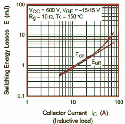
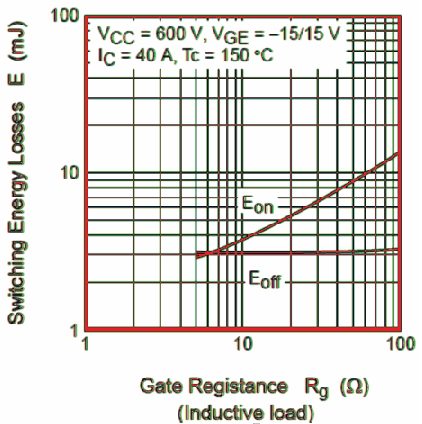
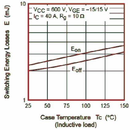
The factors Eon and Eoff are heavily influenced by the collector current, gate resistance, and operating temperature.
Eon (Turn-on energy loss)
The volume of loss developed during the turn-on process of the IGBT for an inductive load, along with the recovery loss at reverse recovery of the diode.
Eon is calculated from the point when gate voltage is powered to the IGBT and the collector current begins travelling, until the point of time when the IGBT is completely transited to the switched ON state
Eoff (Turn-off energy loss
It is the magnitude of loss resulting during the turn-off period for inductive loads, which includes the tail current.
Eoff is measured from the point where the gate current is just cut off and the collector-emitter voltage begins climbing, until the point of time where the IGBT reaches a complete switched OFF state.
How IGBTs are Categorized
IGBTs can be categorized into two types: N-channel and P-channel. Let's discuss each type and their operation:
N-Channel IGBT (Enhancement Mode): In an N-channel IGBT, the main conduction path consists of an N-channel MOSFET and a PNP bipolar transistor.
The MOSFET section controls the IGBT's conductivity, while the bipolar transistor provides voltage amplification. The IGBT is normally in an off state when no voltage is applied to the gate terminal.
To turn on the IGBT, a positive voltage is applied to the gate terminal, which creates an electric field that allows the flow of majority charge carriers (electrons) in the N-channel, thus enabling current conduction.
This positive gate voltage enhances the conductivity of the N-channel, hence the term "enhancement mode."
P-Channel IGBT (Enhancement Mode): In a P-channel IGBT, the main conduction path consists of a P-channel MOSFET and an NPN bipolar transistor.
The MOSFET controls the conductivity, while the bipolar transistor provides voltage amplification. The P-channel IGBT is normally in an off state when no voltage is applied to the gate terminal.
To turn on the P-channel IGBT, a negative voltage is applied to the gate terminal.
The negative gate voltage enhances the conductivity of the P-channel, allowing current to flow through the device.
Both N-channel and P-channel IGBTs operate in enhancement mode, which means they require a gate voltage above a certain threshold to turn on and conduct current.
This characteristic allows for efficient control of the IGBT's switching behavior and power flow in various applications.
It's worth noting that enhancement mode IGBTs are voltage-controlled devices, meaning the gate voltage determines their operating state.
Other IGBT variants, such as depletion mode IGBTs, can operate without an external gate voltage but are less commonly used.
Overall, N-channel and P-channel IGBTs are important components in power electronics, providing high voltage and current capabilities with efficient switching characteristics.
Summary
The insulated-gate bipolar transistor (IGTB) device is a type of three-terminal power semiconductor device which are basically used as electronic switch and is also known for providing a combination of extremely fast switching and high efficiency in the more newer devices.
IGBTs for High Current Applications
A range of modern appliances such as VFDs (Vaiable Frequency Drives), VSFs (variable speed refrigerators), trains, stereo systems with switching amplifiers, electric cars, and air conditioners use insulated-gate bipolar transistor for switching the electric power.

Symbol of depletion mode IGBT
In case the amplifiers use insulated-gate bipolar transistor often synthesize waveforms which are complex in nature along with low-pass filters and pulse width modulation; as insulated-gate bipolar transistor are basically design to turn on and off on a fast and rapid pace.
The pulse repetition rates are boasted by the modern devices which consist of switching application and fall well within the ultrasonic range which are the frequencies which are ten times higher than the highest audio frequency handled by the device when the devices is used in the form of an analog audio amplifier.
The MOSFETs consisting of high current and characteristics of a simple gate-drive is combined with the bipolar transistors which has low-saturation-voltage capacity by the IGTB.
IGBTs are a Combination of BJT and Mosfet
A single device is made by IGBT by combining the bipolar power transistor which acts as a switch and an isolated gate FET which acts as the control input.
The insulated-gate bipolar transistor (IGTB) is majorly used in applications which consists of multiple devices which are placed in parallel to each other and most of the times have capacity of handling very high current which are in the range of hundreds of amperes along with a 6000V of blocking voltage, which in turn is equal to hundreds of kilowatts use medium to high power such as induction heating, switched-mode power supplies, and traction motor control. Insulated-gate bipolar transistors which are large in size.
IGBTs are the Most Advanced Transistors
Insulated-gate bipolar transistor (IGTB) is a new and recent invention of the time.
The first-generation devices which were invented and launched in 1980s and the early years of 1990s were found to have slow switching process relatively and are prone to failure through different modes such as latchup (where the device will continue to be switched on and not turn off till the current keeps on flowing through the device), and secondary breakdown (where when high current flows through the device, a localized hotspot present in the device goes into thermal runaway and as a result burns the device).
There was a lot of improvement observed in the second-generation devices and the most new devices on the block, the third-generation devices are considered even better than the first tow generation devices.
New Mosfets are Competing with IGBTs
The third-generation devices consist of MOSFETs with speed rivaling, and tolerance and ruggedness of excellent level.
The devices of second and third generation consists of pulse rating which are extremely high which make them very useful in order to generate large power pulses in various areas such as plasma physics and particle.
Thus the second and third generation devices have superseded mostly all the older devices such as triggered spark gaps and thyratrons used in these areas of plasma physics and particle.
These devices also hold attraction for the hobbyist of high-voltage due to their properties of high pulse ratings and availability in the market at low prices.
This enables the hobbyist to control huge amounts of power in order to drive devices such as coil-gums and Tesla coils.
Insulated-gate bipolar transistors are available at affordable price range and thus act as an important enabler for hybrid cars and electric vehicles.
Courtesy: Renesas


With over 50,000 comments answered so far, this is the only electronics website dedicated to solving all your circuit-related problems. If you’re stuck on a circuit, please leave your question in the comment box, and I will try to solve it ASAP!