In this post I will elaborately explain how to build a simple LM317 based adjustable power supply circuit using minimum number of external components.
As the name suggests a variable power supply circuit provides the user with a range of linearly varying output voltages through a manually controlled potentiometer rotation.
A LM317 is a versatile device which helps an electronic hobbyist to build a variable voltage power supply quickly, cheaply and very efficiently.
Introduction
Whether it’s an electronic noob or an expert professional, an adjustable power supply unit is required by everybody in the field.
It is the basic source of power that may be required for various electronic procedures, right from powering intricate electronic circuits to the robust electromechanical devices like motors, relays etc.
A variable power supply unit is a must for every electrical and electronic work bench and it’s available in a variety of shapes and sizes in the market and also in the form of schematics to us.
These may be built using discrete components like transistors, resistors etc. or incorporating a single chip for the active functions.
No matter what the type may be, a power supply unit should incorporate the following features to become a universal and reliable with its nature:
Essential Features
- It should be fully and continuously adjustable with its voltage and current outputs.
- Variable current feature can be taken as an optional feature because it’s not an absolute requirement with a power supply, unless the usage is in the range of critical evaluations.
- The voltage produced should be perfectly regulated.
With the advent of chips or ICs like LM317, L200, LM338, LM723, configuring power supply circuits with variable voltage output with the above exceptional qualities has become very easy nowadays.
How to Use LM317 for Producing a Variable Output
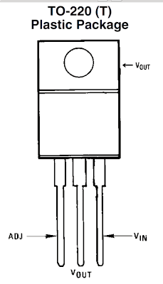
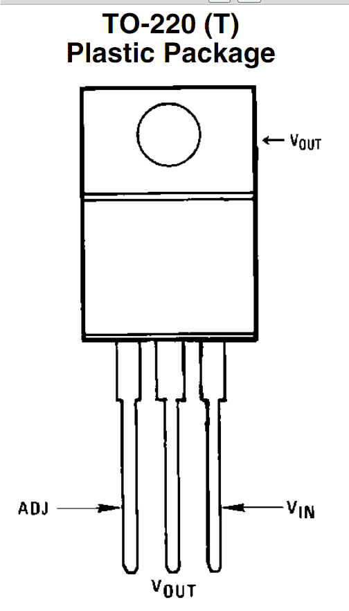
Here I have explained how to construct a simplest power supply circuit using the IC LM317. This IC is normally available in TO-220 package and has three pin outs.
The pin outs are very easy to understand, since it consists of an input, an output and an adjustment pins that just needs to be wired up with the relevant connections.
The input pin is applied with a rectified DC input, preferably with the maximum tolerable input, that’s 24 volts as per the specs of the IC.
The output is received from the “out” pin of the IC while the voltage setting components are connected around the adjustment pin.
How to Connect LM317 in a Adjustable Voltage Power Supply Design
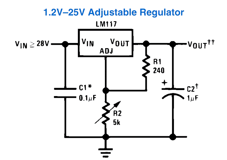
As can be seen the diagram, the assembly needs hardly any components and is in fact a child’s play to get everything in place.
Adjusting the pot produces a linearly varying voltage at the output that may be right from 1.25 volts to the maximum level supplied at the input of the Ic.
Though the shown design is the simplest one and therefore includes only a voltage control feature, a current control feature can also be included with the IC.
Output Voltage Formula
The output voltage (Vout) of the LM317 can be calculated through the two external resistors, R1 and R2, using the formula:
Vout = 1.25 * (1 + R2 / R1)
Where:
- 1.25V is the reference voltage between the Adjust and Output pins.
- R1 is the resistor between the Output pin and the Adjust pin (typically 240Ω).
- R2 is the resistor between the Adjust pin and ground.
Current Through Resistor R1
The current I1 through resistor R1 is approximately:
I1 = 1.25 / R1
If R1 = 240Ω, the current is:
I1 ≈ 5.21 mA
Adjusting the Output Voltage
To set a desired output voltage we can choose the resistors R1 and R2 accordingly. For example if R1 = 240Ω and you want Vout = 5V then you can rearrange the formula for Vout to solve for R2:
5V = 1.25V * (1 + R2 / 240Ω)
Solving for R2 gives:
R2 = 720Ω
Maximum Output Voltage
The output voltage is limited by the input voltage and the LM317's dropout voltage, which is typically around 3V. The maximum output voltage (V_out) is:
Vout = Vin - Vdropout
For example if Vin = 12V and the dropout voltage is 3V then maximum output voltage would be:
Vout = 12V - 3V = 9V
Power Dissipation in the LM317
The LM317 dissipates power as heat, and this power dissipation (Pdiss) is calculated as:
Pdiss = (Vin - Vout) * Iout
Where:
- Vin is the input voltage.
- Vout is the output voltage.
- Iout is the output current.
For example if Vin = 12V, Vout = 5V, and Iout = 1A, then power dissipated by the LM317 would be:
Pdiss = (12V - 5V) * 1A = 7W
Adding a Current Control Feature
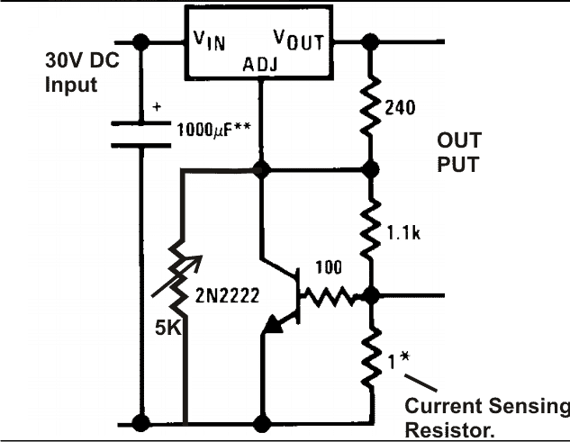
The figure above shows, how the IC LM317 can be effectively used for producing variable voltages and currents, as desired by the user.
The 5K pot is used for adjusting the voltage, whereas the 1 Ohm current sensing resistor is selected appropriately to acquire the desired current limit.
Enhancing with High Current Output Facility
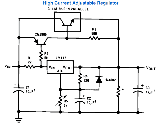
The IC can be further enhanced for producing currents higher than its rated values. The diagram below shows how the IC 317 can be used for producing more than 3 amps of current.
LM317 Variable Voltage, Current Regulator
Our versatile IC LM317/338/396 may be used as an adjustable voltage and current regulator through simple configurations.
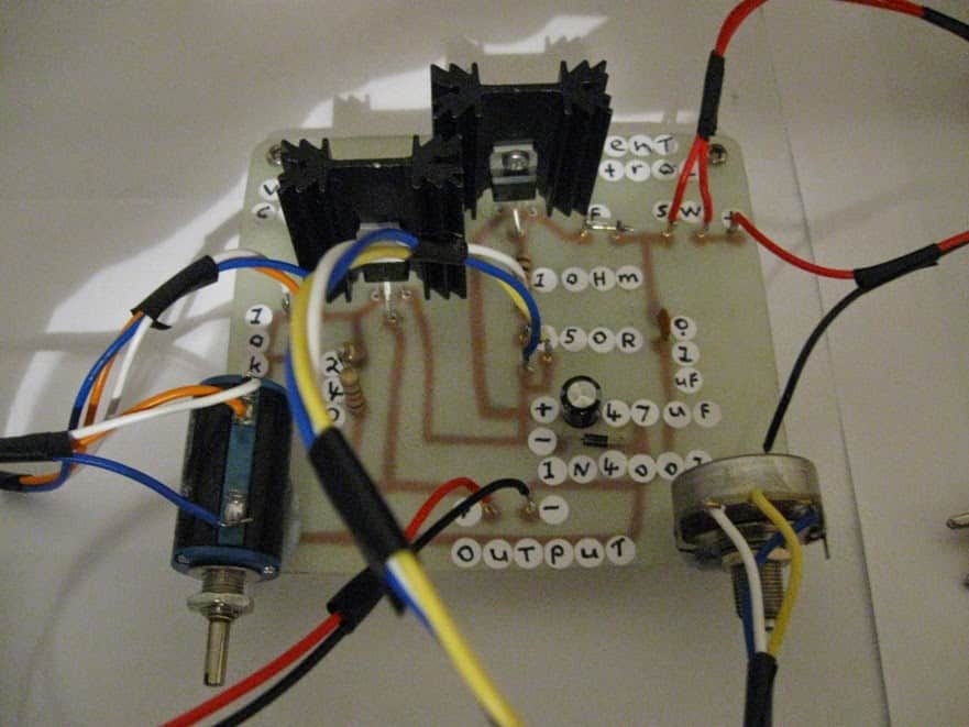
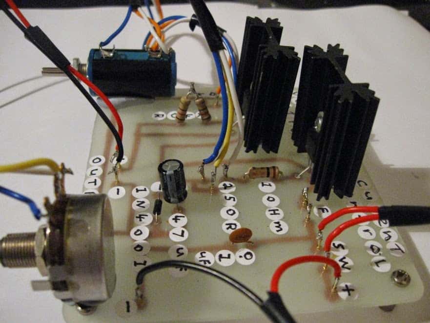
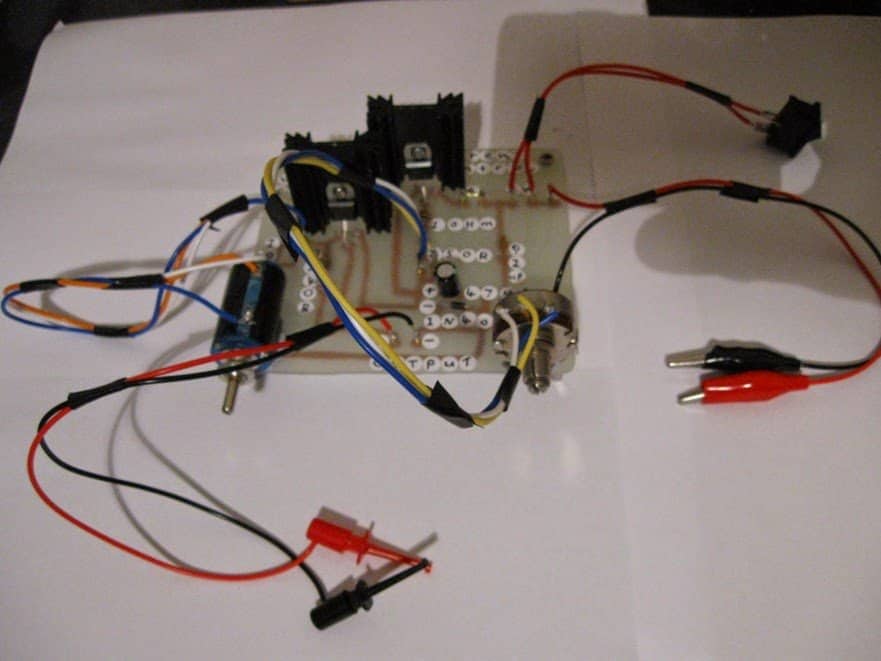
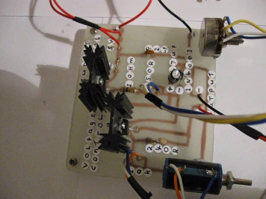
The idea was built and tested by one of the avid readers of this blog Mr. Steven Chiverton and used for driving special laser diodes which are known to have stringent operating specifications, and could be driven only through specialized driver circuits.
The discussed LM317 configuration is so accurate that it becomes ideally suitable for all such specialist current and voltage regulated applications.
Circuit Operation
Referring to the shown circuit diagram, the configuration looks pretty straightforward, two LM317 IC s can be seen, one configured in its standard voltage regulator mode and the other in a current control mode.
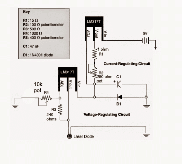
To be precise the upper LM317 forms the current regulator stage while the lower acts like a voltage controller stage.
The input supply source is connected across the Vin and ground of the upper current regulator circuit, the output from this stage goes to the input of the lower LM317 variable voltage regulator stage.
Basically both the stages are connected in series for implementing a complete foolproof voltage and current regulation for the connected load which is a laser diode in the present case.
R2 is selected to acquire a range of around 1.25A max current limit, the minimum allowable being 5mA when the full 250 ohms is set in the path, meaning the current to the laser may be set as desired, anywhere between 5mA to 1 amp.
Calculating the Output Voltage
The output voltage of a LM317 power supply circuit could be determined with the following formula:
VO = VREF (1 + R2 / R1) + (IADJ × R2)
where is = VREF = 1.25
Current ADJ is usually around 50 µA and therefore too negligible in most applications. You can ignore this.
Calculating Current Limit
The above is calculated by using the following formula:
R = 1.25/max allowable current
The current controlled voltage acquired from the upper stage is next applied to the lower LM317 voltage regulator circuit, which enables the desired voltage to be set anywhere from 1.25V to 30V, here the max range being 9V since the source is a 9V battery. This is achieved by adjusting R4.
The discussed circuit is assigned to handle not more than 1.5amps, if higher current is required, both the ICs may be replaced with LM338 for obtaining a max 5amp current or LM396 for a max of 10amp current.
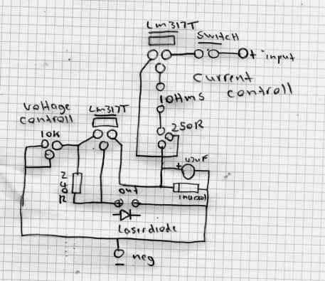
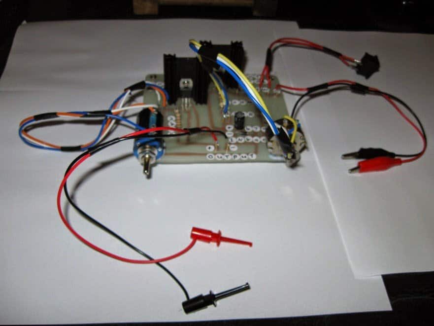
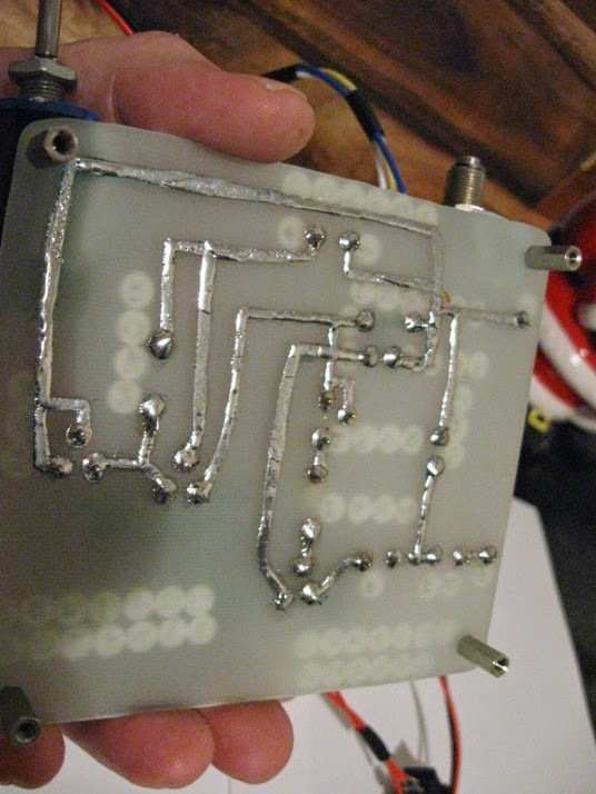
The following lovely pictures were sent by Mr. Steven Chiverton, after the circuit was built and verified successfully by him.
Prototype Images
Upgrading LM317 with Push Button Voltage Control
So far we have learned how to configure an LM317 for producing adjustable output using a pot, now I have explained how push buttons may be used for enabling digitally controlled voltage selection.
We eliminate the use of mechanical pot and replace it with a couple of push buttons for the up/down selection of the desired voltage levels.
The innovation converts the traditional LM317 power supply design into a digital power supply design, by eliminating the low tech potentiometer which might be prone to wear and tear in the long run resulting in erratic operations and incorrect voltage outputs.
The modified LM317 design which would be allow it to respond to the push button selections can be seen in the following diagram:
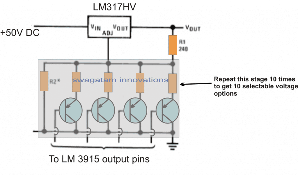
The R2 resistors associated need to be calculated with respect to R1 (240 ohms) for setting up the intended push button selected voltage outputs.
High Current LM317 Bench Power Supply
This high current LM317 power supply can be used universally for any application that requires a high quality regulated high current DC supply, such as car sub woofer amplifiers, battery charges etc.
This power supply is designed to be as versatile as feasible, while also ensuring that the parts count stays low and affordable.
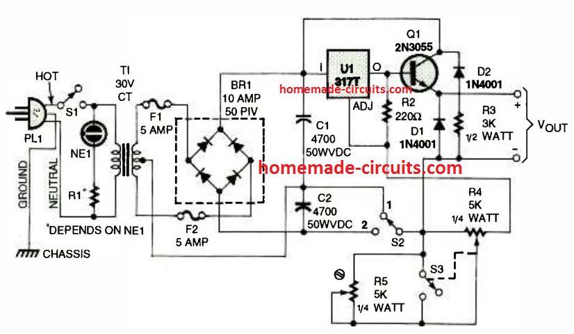
This simple LM317 fixed os adjustable voltage supply satisfies the conditions superbly and is capable of delivering up to 10 amps.
The voltage output is governed by the circuit stage containing R4, R5 and S3; observe that switch S3 is a part of R4.
For getting a fixed voltage output, R4 must be determined for getting zero ohms (fully counter-clockwise). In this situation, switch S3 should be in the open position.
The preset R5 should in that case be tweaked so that the circuit generates a 12 volt output (or anything your personal application requires).
To have an variable output, R4 can be flipped clockwise, with S3 in the closed position, and getting rid of R5 from the circuit.
The output voltage can now be operated by the R4 resistor solely. When the position of SPDT switch S2 is in 1, the highest output current can be accomplished having the two halves of T1 supplying current to the filter stage, in order to increase the overall current output 2 times more.
Having said that, the highest output voltage will be reduced by 50% in this position. It really is a much productive setting considering that the power transistor does not have to drop a significant amount of potential.
In position 2, the maximum voltage practically equals the power specifications of T1. Here, we employed a 24 volt center-tapped transformer for T1.
Lastly, D1 and D2 had been incorporated to safeguard the LM317 IC in case power was switched off with an inductive load at the output
References: http://www.ti.com/lit/ds/symlink/lm317.pdf
https://en.wikipedia.org/wiki/LM317
