In this post I have explained various parameters that must be considered while designing a MOSFET power amplifier circuit. We also analyze the difference between bipolar junction transistors (BJT) and MOSFET characteristics and understand why MOSFETS are more suitable and efficient for power amplifier applications.
Contributed by Daniel Schultz
Overview
When designing a power amplifier is considered in the range of 10 to 20 watts, integrated circuit or IC based designs are normally preferred due to their sleek size and low component count.
However, for higher power output ranges a discrete configuration is considered a much better choice, since they offer higher efficiency and flexibility for the designer with regards to power output selection.
Earlier, power amplifiers using discrete parts depended on bipolar transistors or the BJTs. However, with the advent of sophisticated MOSFETs, BJTs were slowly replaced with these advanced MOSFETs for achieving extremely high power output and amazingly limited space and scaled down PCBs.
Although, MOSFETs may look an overkill for designing medium sized power amplifiers, these can be effectively applied for any size and power amplifier specifications.
Disadvantages of using BJT in Power Amplifiers
Although bipolar devices work extremely well in high end audio power amplifiers, they include a few disadvantages that actually led to the introduction of advanced devices like MOSFETs.
Perhaps the biggest disadvantage of bipolar transistors in Class B output stages is the phenomenon referred to as the runaway situation.
BJTs include a positive temperature coefficient and this specifically gives rise to a phenomenon called thermal runaway, causing a potential damage of the power BJTs due to overheating.
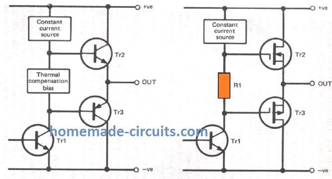
The left side figure above exhibits the essential set up of a standard Class B driver and output stage, employing TR1 like a common emitter driver stage and Tr2 along with Tr3 as the complementary emitter follower output stage.

Function of Amplifier Output Stage
To design a working power amplifier, it is important to configure its output stage correctly.
The objective of the output stage is primarily to provide current amplification (the voltage gain staying no more than unity) in order that the circuit may supply the high output currents essential for driving a loudspeaker in higher volume level.
- Referring to the left side BJT diagram above, Tr2 works like a output current source during the positive going output cycles while Tr3 supplies the output current during the negative output half cycles.
- The basic collector load for a BJT driver stage is designed with a constant current source, which provides enhanced linearity as opposed to the effects achieved with a simple load resistor.
- This occurs due to differences in gain (and accompanying distortion) that happen whenever a BJT works within a wide range of collector currents.
- Applying a load resistor inside a common emitter stage with large output voltage swings can undoubtedly trigger an extremely huge collector current range and large distortions.
- The application of a constant current load doesn't entirely get rid of distortion, because the collector voltage does naturally fluctuate, and the transistor gain might to some extent depend on the collector voltage.
- Nevertheless, as gain fluctuations due to collector voltage variations tend to be fairly minor, low distortion much lower than 1 percent is quite achievable.
- The bias circuit connected between the bases of the output transistors is necessary to take the output transistors to the position where they are just at the conducting threshold.
- In case this does not happen, little variations in the collector voltage of Tr1 might be unable to get the output transistors into conduction and may not allow any kind of improvement in output voltage!
- Higher voltage variations at Tr1’s collector might generate a corresponding changes in the output voltage, but this would likely miss out the starting and finishing portions of each half cycle of the frequency, giving rise to serious “crossover distortion" as it is normally referred to.
Crossover Distortion Issue
Even if the output transistors are taken to the conduction threshold doesn't completely remove crossover distortion since the output devices present relatively small amounts of gain while functioning at reduced collector currents.
This provides a moderate but undesirable kind of crossover distortion. Negative feedback could be utilized to beat crossover distortion naturally, however to achieve excellent results it is actually essential to employ a reasonably high quiescent bias over the output transistors.
It is this large bias current which causes complications with thermal runaway.
The bias current causes heating up of the output transistors, and because of their positive temperature coefficient this causes bias current to increase, generating even more heat and a resultant further elevation in the bias current.
This positive feedback thus supplies a gradual rise in bias until the output transistors get too hot and are eventually burned.
In an effort to protect against this the bias circuit is facilitated with an in-built temperature sensing system, which slows up the bias in case higher temperature is detected.
Therefore, as the output transistor warms up the bias circuit is impacted by the generated heat, which detects this and stops any consequent upsurge in the bias current.
Practically, the bias stabilization may not be ideal and you may find little variations, however, a properly configured circuit may normally exhibit quite a sufficiently enough bias stability.
Why MOSFETs Work more Efficiently than BJTs in Power Amplifiers
In the following discussion I will try to explain why MOSFETs work better in power amplifier designs, compared to BJTs.
Similar to BJTs, if employed in a Class B output stage, MOSFETs also demand a forward bias to overcome crossover distortion.
Having said that, because power MOSFETs possess a negative temperature coefficient at currents of close to 100 milliamps or more (and a slight positive temperature coefficient in lower currents) it allows a less complicated Class B driver and output stage, as demonstrated in the following figure.
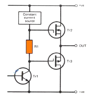
The thermally stabilized bias circuit could be substituted with a resistor because the temperature characteristics of power MOSFETs incorporates an in-built thermal control of the bias current at around 100 milliamps (which is approximately is the the best suited bias current).
An additional challenge experienced with BJTs is the rather low current gain of only 20 to 50. This can be quite insufficient for medium and high power amplifiers. Due to this it requires an extremely powerful driver stage.
The typical approach to solve this issue is to make use of a Darlington Pairs or an equivalent design to provide an adequately high current gain, so that it allows the employment of a low power driver stage.
Power MOSFETs, just like any FET device, tend to be voltage operated devices rather than current operated.
A power MOSFET's input impedance is typically very high which allows negligible input current draw with low working frequencies.
However, at high working frequencies the input impedance is a lot lower because of the relatively high input capacitance of approximately 500 pf.
Even with this high input capacitance a working current of hardly 10 milliamps becomes just enough through the driver stage, although the peak output current could be around one thousand times this quantity.
An additional problem with bipolar power devices (BJT) is their somewhat sluggish switching time. This tends to create a variety of issues, such as slew triggered distortion.
This is when a powerful high frequency signal could demand a switching output voltage of let's say 2 volts per microsecond, while the BJT output stage may possibly allow a slew rate of only a volt per microsecond.
Naturally, the output will struggle to deliver a decent reproduction of the input signal, leading to an unavoidable distortion.
An inferior slew rate may also give an amplifier an undesirable power bandwidth, with the highest achievable power output dropping significantly at higher audio frequencies.
Phase Lag and Oscillations
Another concern is the phase lag that takes place via the amplifier's output stage with high frequencies, and which could cause the feedback over the negative feedback system turning into positive instead of negative at extremely high frequencies.
Should the amplifier possess sufficient gain at such frequencies the amplifier may go into an oscillating mode, and lack of stability will continue to be noticeable even if the gain of the circuit is not ample to trigger an oscillation.
This issue could be corrected by adding elements to roll-off the circuit's high frequency response, and by incorporating phase compensation elements. However, these considerations cuts down the efficiency of the amplifier at high input signal frequencies.
MOSFETs are Faster than BJTs
While designing a power amplifier we must remember that the switching speed of power MOSFETs is generally around 50 to 100 times faster than a BJTs. Therefore, complications with inferior high frequency functionality is easily overcome by employing MOSFETs instead of BJTs.
It is actually possible to create configurations without any frequency or phase compensation parts yet still maintain excellent stability, and include a performance level that is retained for frequencies well past the high frequency audio limit.
Yet another difficulty experienced with bipolar power transistors is secondary breakdown. This refers to a kind of a specific thermal runaway that creates a “hot zone” within the device which results in a short circuit across its collector/emitter pins.
To ensure this does not happen, the BJT needs to be operated exclusively inside specific ranges of collector current and voltage. To any audio amplifier circuit this situation usually implies that the output transistors are forced
to work well inside their thermal restrictions, and the optimum output power obtainable from the power BJTs is thus significantly reduced, much lower than their highest dissipation values actually allow.
Thanks to MOSFET's negative temperature coefficient at high drain currents these devices do not have problems with secondary breakdown.
For MOSFETs, the maximum allowable drain current and drain voltage specs are practically just limited by their heat dissipation functionality. Hence, these devices become specifically well suited for high power audio amplifier applications.
MOSFET Disadvantages
Despite of the above facts, MOSFET also do have a few drawbacks, which are relatively less in number and insignificant. Initially MOSFETs had been highly expensive compared to a matching bipolar transistors.
However, the difference in the cost has gotten a lot smaller nowadays When we consider the fact that MOSFETs makes it possible for for complex circuitry to get much simpler and an indirect significant reduction in cost, makes the BJT counterpart quite trivial even with its low cost tag.
Power MOSFETs often feature an increased open loop distortion than BJTs.
However, due to their high gain and fast switching speeds, power MOSFETs allow the use of a high level of negative feedback across the whole audio frequency spectrum, offering unparalleled closed loop distortion efficiency.
An additional drawback involved with power MOSFETs is their lower efficiency compared to BJTs when employed in the output stages of standard amplifier.
The reason behind this is a high power emitter follower stage which generates a voltage drop as high as around 1 volt between the input and output, although there exists a loss of a some volts across the input/output of a source follower stage.
There isn't an easy approach to solve this problem, however this appears to be a small reduction in efficiency, which shouldn't be taken into account, and could be ignored.
Understanding a Practical MOSFET Amplifier Design
Figure below exhibits the circuit diagram of a functional 35 watt power MOSFET amplifier circuit. Except the MOSFET's application in the amplifier's output stage, everything basically looks quite like a very common MOSFET amplifier design.
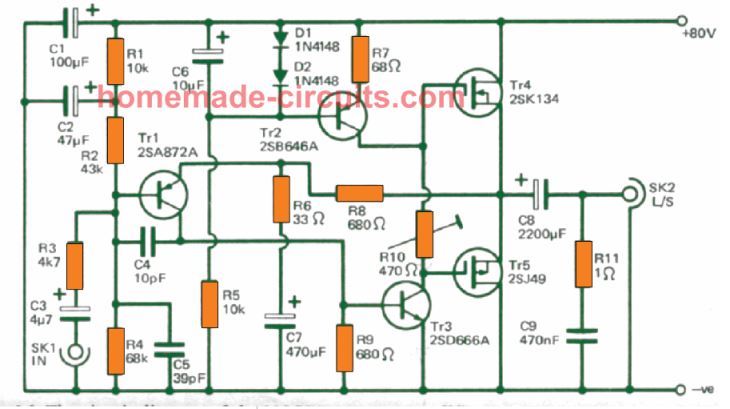
- Tr1 is rigged as a common emitter input stage, directly connected to the Tr3 common emitter driver stage. Both of these stages offer the total voltage gain of the amplifier, and include a extremely large total gain.
- Tr2 along with its attached parts create a simple constant current generator which has a marginal output current of 10 milliamps. This works like the main collector load for Tr3.
- R10 is employed to establish the correct quiescent bias current via the output transistors, and as discussed previously, the thermal stabilization for the bias current is not really accomplished in the bias circuit, but rather it is delivered by the output devices themselves.
- R8 delivers practically 100% negative feedback from the amplifier output to Tr1 emitter, allowing the circuit just around an unity voltage gain.
- Resistors R1, R2 and R4 work like a potential divider network for biasing the amplifier input stage, and consequently the output also, to roughly around half the supply voltage. This enables highest achievable output level before clipping and the start of critical distortion.
- R1 and C2 are used like a filter circuit that cancels hum frequency and other forms of potential noises on the supply lines from entering the amplifier input via the bias circuit.
- R3 and C5 act like an RF filter which prevents RF signals busting right from input to output, causing audible disturbances. C4 also aids to solving the same issue by rolling-off the amplifier's high frequency response effectively over the upper audio frequency limit.
- To ensure that the amplifier gets a good voltage gain at audible frequencies it becomes essential to decouple the negative feedback to some extent.
- C7 fulfils the role of the decoupling capacitor, while the R6 resistor limits the quantity of feedback which is cleaned up.
- The circuit's voltage gain is approximately determined by dividing R8 by R6, or around 20 times (26dB) with the assigned part values.
- The amplifier's maximum output voltage will be 16 volts RMS, which allows an input sensitivity of roughly around 777mV RMS for achieving a full output. The input impedance could be more than 20k.
- C3 and C8 are employed as the input and output coupling capacitors respectively. C1 enables decoupling for the supply DC.
- R11 and C9 exclusively serve to facilitate and control stability of the amplifier, by working like the popular Zobel network, which are often found around the output stages of most semiconductor power amplifiers designs.
Performance Analysis
The prototype amplifier appears to perform incredibly well, specifically only once we notice the fairly simple design of the unit.
The shown MOSFET amplifier design circuit will happily output a 35 watts RMS into an 8 ohm load.
- The total harmonic distortion will not be more than around 0.05%. The prototype was analyzed only for signal frequencies around 1 kHz.
- However the circuit's open loop gain was found to be practically constant within the entire audio frequency range.
- The closed loop frequency response was measured at -2 dB with approximately 20 Hz and 22 kHz signals.
- The amplifier's signal to noise ratio (without a speaker connected) had been higher than the figure of 80 dB, though actually there may be a possibility of a tiny quantity of mains hum from the power supply being detected on the speakers, but the level may be too small to hear in normal conditions.
Power Supply
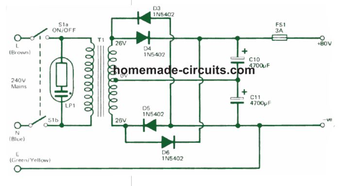
The image above demonstrates an appropriately configured power supply for the 35 watt MOSFET amplifier design. The power supply may be adequately powerful to handle a mono or a stereo model of the unit.
The power supply is actually made up of an efficient a couple of push-pull rectifier and smoothing circuits which have their outputs attached in series to provide a total output voltage corresponding to twice the potential applied by a individual rectifier and capacitive filter circuit.
Diodes D4, D6 and C10 constitute one particular portion of the power supply while the second section is delivered by D3, D5 and C11. Each of these offer slightly below 40 volts without a load connected, and a total voltage of 80 V unloaded.
This value may drop to approximately 77 volts when the amplifier is loaded by a stereo input signal with a quiescent state operational, and to just around 60 volts when two amplifier channels are operated at full or maximum power.
Construction Hints
An ideal PCB layout for the 35 watt MOSFET amplifier is demonstrated in the Figures below.
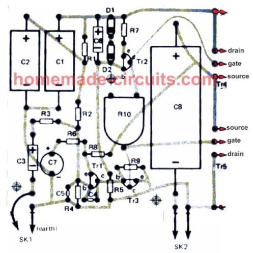

This is meant for one channel of the amplifier circuit, so naturally two such boards have to be assembled when a stereo amplifier becomes necessary.
The output transistors are certainly not fitted on the PCB, rather over a large finned type.
It is not necessary to use mica insulation kit for the transistors while fixing them on the heatsink.
This is because the MOSFET sources are directly connected to their metal tabs, and these source pins have to be anyway remain connected to each other.
However, since they are not insulated from the heatsink it may be truly vital to ensure that the heatsinks do not come into an electrical contact with various other parts of the amplifier.
Also, for a stereo implementation the individual heatsinks employed for the a pair of amplifiers should not be allowed to get into an electrical proximity with each other. Always make sure to employ use shorter leads of a maximum of around 50 mm to hook up the output transistors with the PCB.
This is specifically crucial for the leads that connect with the gate terminals of the output MOSFETs.
Due to the fact that Power MOSFETs have high gain at high frequencies, longer leads may severely affect the stability response of the amplifier, or even trigger an RF oscillation which may in turn cause a permanent damage to the power MOSFETs.
Having said that, practically you may find hardly any difficulty in preparing the design to ensure that these leads are effectively held shorter.
It may be important to note that C9 and R11 mounted outside the PCB, and are simply connected in series across the output socket.
Power Supply Construction Tips
The power supply circuit is built by applying a point-to-point type wiring, as indicated in the below figure.
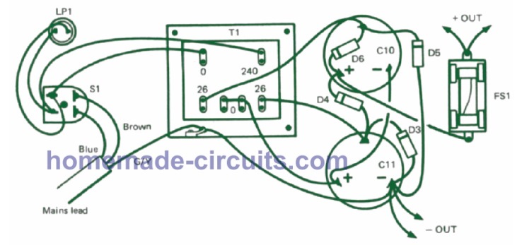
This actually looks pretty self-explanatory nevertheless it is ensured that the capacitors C10 and C11 both types consist of a dummy tag.
In case they aren't it can be crucial to employ a tag-strip to enable a few connection ports. A solder-tag is Clipped to one particular mounting bolts of T1, which offers a chassis connection point for the mains AC earth lead.
Adjustment and Settings
- Be sure to comprehensively examine the wiring connections prior to switching ON the power supply, because wiring mistakes could cause costly destruction and might certainly be hazardous.
- Before you switch on the circuit make sure to trim R10 to get minimal resistance (rotate in complete anticlockwise direction).
- With FS1 momentarily taken out and a multimeter fixed to measure 500mA FSD attached over the fuse holder, a reading of around 20mA must be seen on the meter while the amplifier is powered on (this may be 40mA when two channel stereo is employed).
- In case you find the meter reading substantially dissimilar to this switch off power immediately and re examine the entire wiring. On the contrary, if all is good, slowly move R10 to maximize the meter reading up to a value of 100mA.
- If a stereo amplifier is desired, R10 across both the channels must be tweaked to get the current draw up to 120mA, then R10 in the 2nd channel must be fine-tuned to increase the current usage to 200mA. Once these are accomplished, your MOSFET amplifier is ready to use.
- Take extreme care not to touch any of the AC mains connections while doing the setting up procedures for the amplifier.
- All the uncovered wiring or cable connections which may be at the AC mains potential should be properly insulated before linking the device to the mains supply.
- Needless to say, as with every AC operated circuit, it should be enclosed within a sturdy cabinet which could only be unscrewed with the help of dedicated screwdriver and other set of instruments, to ensure that there isn't any quick means to reach the hazardous mains wiring, and accidents are safely eliminated.
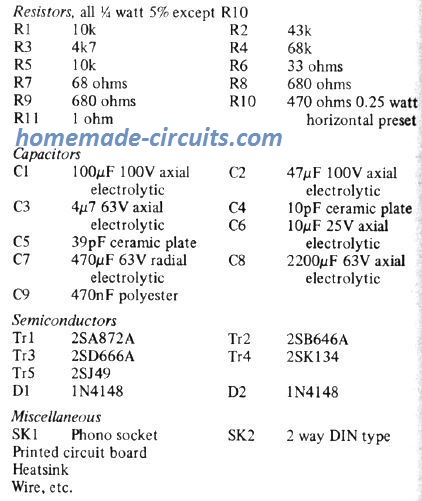
Parts List for the 35 watt MOSFET Power Amplifier

120W MOSFET Amplifier Application Circuit
Depending on the power supply specifications, the practical 120 watt MOSFET amplifier circuit is capable of offering an output power of in the range of about 50 and 120 watts RMS into an 8 ohm loudspeaker.
This design also incorporates MOSFETs in the output stage to provide a superior level of overall performance even with the great simplicity of the circuit
The amplifier's total harmonic distortion is no more than 0.05%, but only when the circuit is not over loaded, and the signal to noise ratio is superior to 100dB.
Understanding MOSFET Amplifier Stages
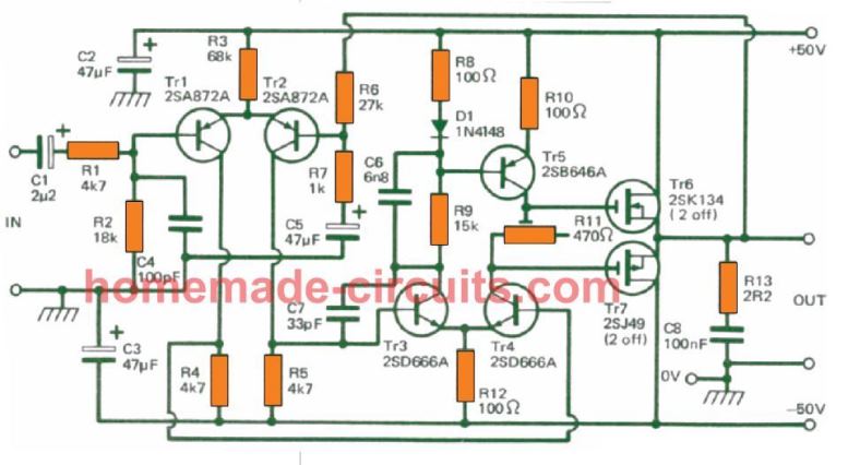
As shown above this circuit is designed with reference to a Hitachi layout. Contrary to the last design, this circuit makes use of DC coupling for the loudspeaker and contains twin balanced power supply with a middle 0V and earth rail.
This enhancement gets rid of the dependency on big output coupling capacitors, as well as the under performance in low frequency performance this capacitor generates. Furthermore, this layout also allows the circuit a decent supply ripple rejection capability.
Besides the DC coupling feature, the circuit design appears pretty distinct from that used in the earlier design. Here, both the input and driver stages incorporate differential amplifiers.
The input stage is configured using Tr1 and Tr2 while the driver stage is dependent on Tr3 and Tr4.
Transistor Tr5 is configured like a constant current collector load for Tr4. The signal path by means of the amplifier commences using input coupling capacitor C1 , along with the RF filter R1/C4. R2 is used for biasing the amplifier's input on the central 0V supply track.
Tr1 is wired as an efficient a common emitter amplifier which has its output directly connected to Tr4 which is applied as a common emitter driver stage.
From this stage onwards the audio signal is linked to Tr6 and Tr7 which are rigged as complementary source follower output stage.
The negative feedback is extracted from the amplifier output and connected with the Tr2 base, and despite of the fact that there's no signal inversion through the Tr1 base to the output of the amplifier, there does exist an inversion across the Tr2 base and the output. It is because Tr2 working like an emitter follower perfectly drives the emitter of Tr1.
When an input signal is applied to the Tr1 emitter, the transistors successfully act like a common base stage.
Therefore, though the inversion does not take place by means of Tr1 and Tr2, inversion does happen through Tr4.
Also, phase change does not occur via the output stage, which means that the amplifier and the Tr2 base tend to be out-of-phase to execute the required required negative feedback. The R6 and R7 values as suggested in the diagram provide a voltage gain of approximately 28 times.
As I have explained from our previous discussions, a small disadvantage of power MOSFETs is they become less efficient than BJTs when they are wired through traditional Class B output stage.
Also, the relative efficiency of power MOSFETs gets rather bad with high power circuits which demand gate/source voltage to be of several voltage for high source currents.
The maximum output voltage swing can be assumed to be equal to the supply voltage minus the maximum gate to source voltage of the individual transistor, and this certainly allows an output voltage swing which may be significantly lower than the supply voltage applied.
A straightforward means of getting higher efficiency would be to basically incorporate a couple of similar MOSFETs attached in parallel across each of the output transistors.
The highest amount of current handled by each output MOSFETs will then be roughly reduced by half, and the maximum source to gate voltage of each MOSFET is lowered appropriately (along with a proportionate growth in the amplifier's output voltage swing).
However, a similar approach does not work when applied to bipolar devices, and this is essentially due to their positive temperature coefficient characteristics.
If one particular output BJT begins drawing excessive current than the other (because no two transistors will have exactly identical characteristic), one device begins getting more hot than the other.
This increased temperature causes the BJT's emitter/base threshold voltage getting reduced, and as a result it begins consuming a much larger portion of the output current.
The situation then causes the transistor to get hotter, and this process continues infinitely until one of the output transistor begins handling all the load, while the other remains inactive.
This kind of problem cannot be seen with power MOSFETs because of their negative temperature coefficient. When one MOSFET begins getting hotter, due to its negative temperature coefficient the incresing heat begins restricting current flow through its drain/source.
This shifts the excess current towards the other MOSFET which now begins getting hotter, and quite similarly the heat causes the current through it to reduce proportionately.
The situation creates a balanced current share and dissipation across the devices making the amplifier working much efficient and reliable.
This phenomenon also allows MOSFETs to be connected in parallel simply by joining gate, source and drain leads together without much calculations or concerns.
Power Supply for 120 watt MOSFET Amplifier
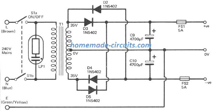
An appropriately designed power supply circuit for the 120 watt MOSFET amplifier is indicated above. This looks much like the power supply circuit for our earlier design.
The only difference being the transformer center tap supply at the junction of the two smoothing capacitors had been initially disregarded.
For the present example this is accustomed to provide the middle 0V earth supply, while the mains earth also hooks up at this junction instead of to the negative supply rail.
You can find fuses being installed across both the positive and negative rails.
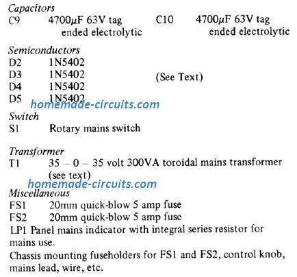
The power output which is delivered by the amplifier largely is dependent on the mains transformer specs. For the majority of requirements a 35 — 0 — 35 volt 160VA toroidal mains transformer should be actually quite enough.
If stereo operation is preferred, the transformer will need to be replaced with a heavier 300 VA transformer.
Alternatively, isolated power supply units could be built using 160VA transformer each for each channel.
This allows a supply voltage of approximately 50 V at quiescent conditions, although at full load this level may drop to a much lower level.
This enables an output of up to around 70 watts RMS to be acquired through 8 ohm rated loudspeakers.
A crucial point to be noted is that the 1N5402 diodes used in the bridge rectifier have a maximum tolerable current rating of 3 amps.
This may be ample for a single channel amplifier, but this may not be sufficient for a stereo version. For a stereo version the diodes must be replaced with 6 amp diodes or a 6A4 diodes.
PCB Layouts
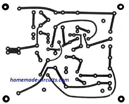
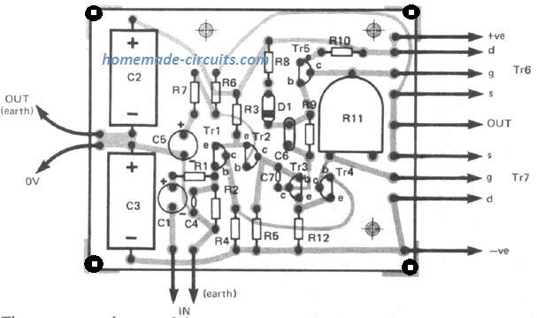
You can find a full fledged PCB, for building your own 120 watt MOSFET amplifier circuit. The indicated 4 MOSFET devices should be attached with large finned heatsinks, which must be rated at minimum 4.5 degree Celsius per watt.
Wiring Precautions
- Make sure to keep the MOSFET pinout terminals as short as possible, which must be no more than around 50 mm in length.
- If you want to keep them a little longer than this, make sure to add a low value resistor (may be a 50 ohm 1/4 watt) with the gate of each of the MOSFETs.
- This resistor will respond with the MOSFET's input capacitance and act like a low pass filter, ensuring a better frequency stability for the high frequency signal input.
- However, at high frequency input signals, these resistors might produce some affect on the output performance, but this may be actually too small and hardly noticeable.
- The transistor Tr6 actually consists of two n-channel MOSFETs connected in parallel, same is for Tr7, which also has a couple of p-channel MOSFETs in parallel.
- To implement this parallel connection, the gate, drain, source of the respective MOSFET pairs are simply joined with one another, that's all it is as simple as that.
- Also, please note that the capacitor C8 and the resistor R13 are installed directly on the output socket, and not assembled on the PCB.
- Perhaps the most effective method of building the power supply is by hard-wiring, as for the power supply as done for the previous amplifier. The wiring is much the same as for this previous circuit.
Adjustments and Settings
- Before powering ON the completed amplifier circuit, make sure to carefully examine every one of the wiring several times.
- Specifically check the power supply wiring and the relevant interconnections across the output power MOSFETs.
- Faults around these connections could quickly lead to permanent damage to the amplifier unit.
- Also, you will need to perform a few prior adjustments before switching ON the completed board.
- Begin by rotating the R11 preset fully anti-clockwise, and do not initially connect a loudspeaker to the output of the unit.
- Next, instead of a loudspeaker, connect your multimeter (set at low voltage DC range) probes across the amplifier output points, and make sure it shows the low quiescent output voltage is available.
- You may find the meter showing fractional voltage or may be no voltage at all, which is also fine.
- In case a large DC voltage is indicated by the meter, you must immediately switch off the amplifier and recheck for any possible mistakes in the wiring.
Conclusion
In the above article we have comprehensively discussed the many parameters which play a crucial role in ensuring the correct and optimal working of a power amplifier.
All these parameters are standard and therefore can be effectively used and applied while designing any MOSFET power amplifier circuit, regardless of the wattage and voltage specifications.
The different characteristics detailed regarding BJT and MOSFETs devices could be used by the designer to implement or customize a desired power amplifier circuit.


With over 50,000 comments answered so far, this is the only electronics website dedicated to solving all your circuit-related problems. If you’re stuck on a circuit, please leave your question in the comment box, and I will try to solve it ASAP!