You can use this simple visible light communication circuit to send audio and digital information through infrared light, beyond a mile away, with extreme precision.
By Sunil Rao
The main features of the light communicator circuit can be understood with the following points:
- Output power = 5 millwatts
- Frequency Modulation Operation with 50 kHz carrier signal
- Bandwidth = 300 to 3000 Hz
- Without lens, the range is around 40 feet.
- With 3 diameter optics or a magnifying lens, the range can be increased over a mile.
The main function of the proposed light communication circuit is to achieve a straight line, point to point transfer of voice or music signals, upto over a mile.
Another great application can be a long-distance "broken beam" security alarm system, where the beam could be laid down over a long restricted zone, and when anybody breaks the line, an alarm is raised.
Understanding the Parameters
Before going through the actual building of the Light beam communicator, let's first discuss a few optical terminology and parameters.
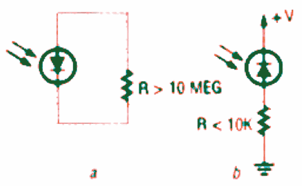
PIN Diode: It is a photosensitive diode with a reaction time of a couple of nanoseconds. It could be employed in the photoconductive mode in which the amount of current passing through it depends on the light incident on it, or when used in the photovoltaic functionality the voltage across it is dependent on light (see Fig. 1).

Phototransistor: It is actually a transistor which has its base current dependent on the light. The collector current is = base current x gain of the device. Reaction time is just around a few microseconds.
Photodarlington: When a couple of transistors in the same package are hooked up in a specific high gain configuration, it constitutes a Darlington. In a photodarlington the first transistor is a phototransistor and the second one is any standard BJT. Response time may be around hundredths of microseconds.
Detector area: It can be defined as the area (in square inches or millimeters) of the diode detector which accumulates the light. The majority of PIN diodes use a plastic casing which works like a straightforward lens and gives a accumulation region of 0.01 to 0.025 square inches. This region is very important while calculating the gain of the lens.
Inverse square law: This is actually the "key element" in almost all optical communications devices. Simply said, it signifies that in case you increase the range across transmitter and the receiver, the capacity of the signal becomes proportionately lesser by the square of the distance. As an example, if you obtain 9 microwatts of power with a 10 feet distance between the transmitter and receiver, you can expect to obtain just one microwatt of energy in case you raise the distance to 30 feet.
Transimpedance amplifier: It is an amplifier having an extremely low input impedance. Often known as current-to-voltage converters, these special amplifiers in many cases can be found in optical devices. Due to their low impedance load these guarantee optimum current through a photodiode. They are able to offer a bandwidth up to a several hundred megahertz.
Lens gain: It is the ratio of the lens area to the detector area. Given that the lens area is bigger than the detector area, a greater amount of light is collected from the lens. Lens losses and focusing errors (which jointly amount to approximately 15%) should be taken into account while calculating the lens gain.
Infrared: It is the area of the light spectrum close to the red color (around 800 nanometers). Many infrared LED's give off at either 880 nanometers or 940 nanometers. The majority of silicon sensors show highest responsiveness at around 900 nanometers. Infrared is employed mainly because almost all red (visible light) LED's don't find it easy to generate a 1 / 2 a milliwatt of power, although numerous IR LED's possess an output of 10 milliwatts or higher.
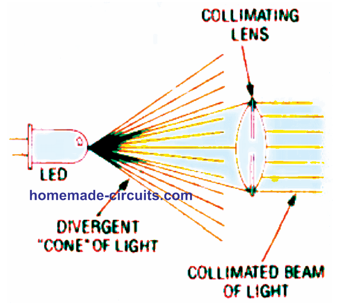
Collimate: This term refers to: aiming in a straight line. Whenever light coming from a source moves through parallel beams rather than with a divergent cone, it is recognized as collimated. Even though it is not possible to create a genuinely collimated beam, the lens of the transmitter makes an attempt to achieve this (see Fig. 2).

Divergence: It is understood as the "dispersing off" of an optical ray. Put simply, a diverging stream of light is the opposite of a collimated beam. Just about all optical rays of light spread out in a divergent manner, some may do this a little more than others. If you are able to create a ray of light having zero divergence (which is impossible), it simply would never comply with the inverse square law.
Meaning, it may be possible to direct a beam of light to an unlimited distance since the energy would be travelling without spreading or dispersing outward.
You will find very less divergence in laser beam lights, compared to other ordinary light sources. Most of the spot lights are designed to have lower level of divergence, while flood lights have a huge amount of divergence (Fig2).
Responsivity: It is determined by the relationship between the optical and the electrical signal of a detector. Generally, this value for a PIN diode can be 0.4 amps to 0.6 amps per watt. Therefore, if a 1 mW light is incident on a PIN diode, we can expect a current outflow of 0.4 mA to 0.6 mA from it. With regard to this attribute the proposed visible light beam communication might work using a current level of 100 pA, or using an optical power of 200 pW.
AC and DC Light: When you switch a LED lamp by toggling it ON and OFF, you are basically generating an AC like light source from the LED lamp. If you illuminate it with a constant DC, then it becomes a DC source of light. This phenomenon is important since most of the light source may have some traces of AC and some DC in them.
The flashlights using incandescent light bulb, exhibit a high quantity of DC light and a low quantity of AC light through them. Our sun light is composed huge amounts of AC as well as DC light in it. Fluorescent lamps emit some DC but a lot of AC.
In the proposed visible light communication circuit, the above phenomenon is crucial because, operating a DC based optical receiver may come across a plenty of AC light sources including sun light, which can rapidly saturate the receiver detection capacity and the actual detection of our AC communication signal can get hampered. To overcome this issue, some sort of light shield will need to be installed which are commonly used in our cameras etc
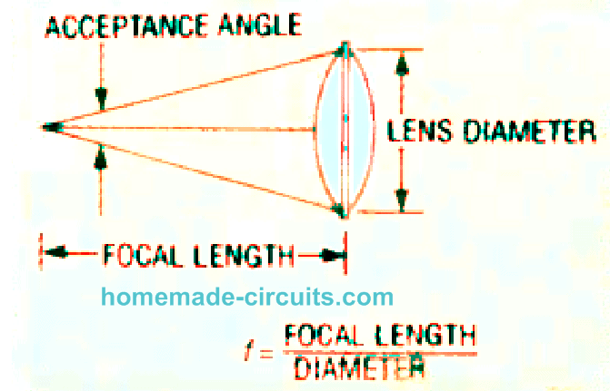
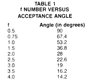
f number or lens speed: In glass lenses the focal length to its diameter ratio is termed as the "f" number (f = fl/d).
Smaller f number determines a faster and more expensive lens. You can easily imagine this figure as the optical "acceptance" angle (Fig3). The feature becomes useful while selecting the transmitter len's collimating function.

In cameras, which are designed to work with a fixed focal length, utilizes one lens that has a bigger diameter and another that has a smaller "f' number for a faster response. This ensures that the larger lens is able to accumulate more quantity of light and the shutter is set to a faster speed than the smaller lens.
Table 1 can be referred for getting the "f" numbers vs. acceptance angles information.

Thermal noise: Even though thermal noise is not actually relevant to optical products for example lenses, the electronic functionality of the optical system could be restricted by thermal noise. Thermal noise is induced in an electrical system through the arbitrary motion of molecules. The thermal current noise (IN) of a resistor can be expressed by the equation:
(IN)2 = 4KTB/R
- where K = Boltzmann's constant (1.38 x 10⁻²³)
- T = temperature in Kelvin (300)
- B = bandwidth in Hertz
- R = resistance in ohms
A 300K resistor powered at around room temperature inside the receiver having a bandwidth of 20 kHz should eihibit a thermal noise current of 33 picoamps. Despite the fact that 33 picoamps probably won't seem like a great deal of current, the noise may boost at the transimpedance amplifier output to as high as approximately 10 microvolts (RMS).
Converting this to peak-to-peak noise provides around 60 microvolts peak-to-peak. In the light communication circuit, the sole amplifier between the transimpedance amplifier and the comparator is actually a differential amplifier using a gain of approximately 50. This amplifier amplifies the 60 microvolts noise and generates around 3 millivolts noise at the optical amp output.
Precise readings confirm a generation of 5 millivolts of noise. This is acceptable since additional noise-producing elements exist in the unit, like the current amplification noise from the 1st transistor. Though just about every transistor generates little noise, the first one generates excessive noise due to its greater signal amplification.
The significance of presenting equations such as this is that they provide us awareness for system enhancement and corrections. If we had no issues of noise, practically endless distances could possibly be reached. Nevertheless, if the signal strength is smaller than the noise, then that can be bad news for the experimenter.
We are able to deal with temperature issue at some level, and the equation indicates that when the temperature is lower, the noise is also lower.
However decreasing the transimpedance resistor temperature even by 100 degrees Kelvin might cause a reduction in the noise power by only a factor of approximately 1.2.
When an optical unit has a specifications of just a small amount of bandwidth of maybe a few hertz, such as a television remote control, we're able to reduce the bandwidth from 20 kHz to 20 Hertz and reduce the noise by a factor of approximately 30. Even while the inverse square rule running against us, that could cause an enhanced range through a factor of around 5.
This kind of reduction in the bandwidth might call for a decent tunable filter, which anyhow can be achieved. Obviously, audio signals directed through a link using a 20 Hz bandwidth wouldn't be identifiable as audio. However, it might enable a Morse-code transmission.
Photodetector: It is a semiconductor device designed to transform light into an electrical signal. All devices like phototransistors, photo SCR's, phototriacs photocells, solar cells, and photodiodes fall under this category of photodetector. Even parts like photoresistors and thermocouples could be generally regarded as varieties of photodetectors.
Phototransistors and photo-Darlington sensors are generally accustomed to detect light. Both of these devices do the job well in case high speed detection is not a necessity.
Normal phototransistor have a switching period of 1 to 5 microseconds. For Darlington types this figure may be around hundreds of microseconds.
PIN Diode Features
- PIN diode was decided as the better option as the detector in this project in the photoconductive mode. Because, they are not restricted by the gain and bandwidth, like the phototransistors.
- PIN diode provide us the unrestricted options for both the above parameters, making it possible for us to develop our personal amplifiers.
- PIN diodes are also extremely "silent." Their noise is practically unreadable by an equipment.
LED's: A light-emitting-diode is a semiconductor device that produces light when connected in the forward biased direction in an electrical circuit.
Selecting the Transmitter LED
You might feel that selecting an LED for this type of projects might be a very uncomplicated thing, however it's not.
Characteristics like power output, wavelength, speed, and beam angle all become crucial while figuring out the right type of LED.
The very first thing to consider is the power output. Having said that, if you fail to achieve the required amount of power into the lens, it can easily get wasted, and if the wavelength selection is incorrect, the detector wouldn't be able to catch it.
Wavelength is Important
By far the most popular wavelengths for infrared equipment are 880 nanometers and 940 nanometers.
The 1st option is to get a properly matching detector and emitter units.
In our light communicator project a 940 nanometers is selected, which is deeper into the infrared than 880 spectrum.
A lot of detectors created for 940 nanometers incorporate a pre-installed visible-light filter. Filters aren't generally used on the 880-nanometer products mainly because this wavelength is close to the visible spectrum and this kind of a narrow filter might be challenging to manufacture in huge volumes.
If you would like manufacture hundreds of these light communication circuits along with optics, you would probably want to invest in emitters with broad yet symmetrical beams.
In this way you would probably get a customized lens developed and manufactured at a modest cost using plastic-type material. This might probably enable you to achieve the most consistent beam and would allow manufacturing in big quantities.
For example, in an IR based remote control, you might like to incorporate an emitter or many emitters to generate an IR "flood" for a specific region. For this , you would like to get an emitter featuring a wide beam.
When, however, you're simply seeking to test what lengths you can make the signal travel, you will require something completely different. Narrow beam angles become important for effective connection with any locally available lens.
Precisely speaking, determining the lowest beam angle among the lenses will save you a lot of money in terms of investments in lenses. The smallest quickly accessible beam angle for an LED is approximately 20 degrees. Whenever a manufacturer suggests this angle, he genuinely implies a "half angle" of 20 degrees, or a solid cone of 40 degrees.
The angle additionally determines the half-power point. For instance, when a manufacturer identifies 5 milliwatts along with a beam angle of 20 degrees, this indicates that if you are able to capture the whole power within a 40-degree cone, you could possibly get hold of 2.5 milliwatts of optical power.
No matter what the situation is,make sure to buy an LED having a tiny beam angle, with the maximum amount of power as possible, and a fair speed.
Function of Lenses
Lenses in optical communicators do what the antennas for RF circuits. The significance of perhaps basic lenses cannot be over-stressed. If a high-frequency RF engineer is able to construct an antenna with 60 dB gain for under 10 dollars, we could have probably witness many satisfied RF technicians!
Considering that the optical world works with extremely tiny wavelengths, a gain of 1000 or 60 dB is not difficult to achieve. You may find this strange, but the dimensions of the lens on the receiver can be very critical, however on the transmitter it isn't so critical.
This is because the receiver does the crucial work to intercept the maximum amount of light that may be possible, therefore the bigger the lens, the more effective it is.
The main objective of the transmitter lens is to collimate the beam, hence just about any lens having the proper "f' number will do the job. The "f" number determines the speed of the lens, and this should be well known to any individual with photography as a leisure activity. This may be understood as the measure of the acceptance angle of the lens.
While transmitting the signal beam, all the LED light which is dispersed away from the cone is lost. A 50-milliwatt LED might be useless if the light "shoots" away at 90 degrees and all those lights which cannot be channelled into the lens is elimiated.
The gain of a lens is actually the ratio of the lens area to the area of the detector. For instance, the area of most PIN diodes is approximately 0.01 square inch. A 2-inch diameter lens will have an area of 3.14 square inches. As a result, the gain of a 2-inch lens will be around 3.14/0.01 or 314.
It must be noted that this lens amplifier does not required any external power to operate, and yet covers infinite bandwidth, without adding any noise to the signal. A device like a lens in the world of electronics can be therefore considered an absolute miracle.
Table 2 exhibits the gain for a few different lens sizes.

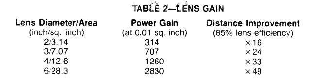
The data here is provided with a consideration that no light is assimilated or reflected by the lens, and the detector is positioned exactly at the focal point of the lens. These considerations can be obviously inconsistent, since even the best quality camera lenses, that are layered with anti-reflective coatings, never allow 100 percent light to pass. There may be ample room here for trials. Several elementary tests revealed that around 85% of the calculative or assumptive gain is achievable.
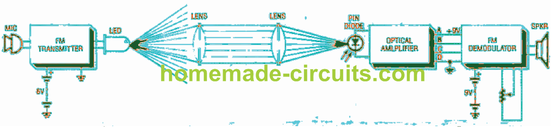
FM Transmitter Circuit
The visible light communication is created using three circuits stages. The first stage is the FM transmitter. The remaining two stages (the optical amplifier and FM demodulator) constitute the receiver.
A block diagram of the circuit is shown in Fig. 4.

The FM transmitter circuit stage, shown in Fig. 5, is made up of a microphone amplifier (Q1 and Q2) and an FM modulator created through a 555 timer (IC1). You can find a couple of setting options, one for the FM center frequency (R11) and the other for adjusting the level of deviation (R4).

Resistor R1 is used for microphones which work with an external power supply, for example the electret type. If an external audio source is used, the input should be restricted to a few millivolts. The IC1 output pin 3 can be tweaked by means of R11 in order that the frequency is set at 50 kHz (20 microseconds).
Using External Modulation Signal
The IC 555 output could be frequency modulated through the use of the upper trip-point voltage reference to pin 5. Despite the fact that it may be impossible to push the frequency too far, deviation of the frequency at around 10% approximately can easily happen. These deviations is actually a function of the signal amplitude applied over the pin 5.
When an external DC modulation voltage induced at pin 5 is turned on and off, this generates an FSK (digital) data. Although the 555 output is rated adequately to drive a power LED, transistor drivers have been incorporated for enabling the operation of many LED's combined.
Resistors R17 and R18 can be seen correctly set up in order to limit the current for the specific LED. Currents as high as 200 milliamps might present no issue for the LED's, however these might drain your batteries rapidly. If a single LED is being used, positioning a 47 ohms in series will allow only around 45 milliamps, typically.
If your system uses two LED's, the series resistor could be changed to a 22 ohms and the current involved will be almost the same. In the actual prototype, it was operated using four AA alkaline type batteries for powering the transmitter.
Optical Amplifier Circuit (Receiver)
The function of the optical amplifier circuit stage, as demonstrated in Fig. 6, is to change the optical signal into electrical signal, limit its bandwidth (to minimize disturbance), and to deliver a differential drive to the comparator.

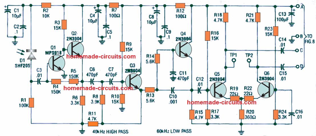
The PIN diode detector (D1) can be seen connected through AC signal with a basic transimpedance amplifier comprising Q1 and Q2. Although the signal is coupled through an AC signal, the biasing for the PIN diode has to be DC coupled. This is accomplished by means of resistors R1 and R2.
If the proposed light communication circuit is operated in a excessive background light condition, resistor R1 may need to be decreased in value to stop DC saturation of the PIN diode. In case the DC voltage across R1 is higher than around 3 volts during functioning, it may be a good idea to reduce the value of R1. The transimpedance resistors (R4 and R5) determine the actual gain of the amplifier. A couple of series resistors were employed rather than just a single since each resistor has its own capacitance across themselves.
By using pair of resistors allows the reduction in the capacitance with a factor of two. All that is needed is to connect the two resistors over the PCB. The transimpedance amplifier output is nothing but its input current multiplied by the transimpedance resistance. For this reason it's occasionally known as current-to-voltage converter.
When you increase the resistance value, the signal also boosts, however the bandwidth diminishes. Because the signal boosts directly in response to the resistance value, and we also have an increasing noise by the square root of the resistance.
It seems sensible to use a resistance that's as big as it possibly can be, provided you continue to have sufficient bandwidth. For this reason Q1 has to be a VHF transistor.
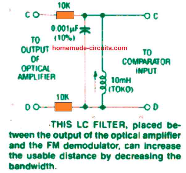
Because the signal's center frequency is at 50 kHz, it's advisable to restrict the optical amp's bandwidth to minimize the overall noise.
Transistor Q3 along with the encircling parts constitute a two-way high-pass filter at around 40 kHz. This gets rid of the low frequency noise, for example like the 50/60 hertz optical noise emitted by our home lights.
Transistor Q4 as well as the connected circuitry create a 60 kHz low-pass filter. This eradicates high-frequency electrical noise for example those emanating from many AM radio stations. When we integrate the low-pass and highpass filters, they give rise to a bandpass filter structured around 50 kHz, having a pass band of approximately 20 kHz.
It may be possible to cut down the noise by creating a narrower filter, between the optical amp's output and the demodulation stage input. The drawback is may be that the narrow filter will need to be tunable, and will require a scope for setting it up.
Transistors Q5 and Q6 are used for designing a differential amplifier which is actually the gain stage of the optical amplifier, apart from Q1.
The function of a differential amplifier is to ensure that a differential signal is avaialble to operate the voltage comparator. It can be great to operate a comparator differentially as you are able to acquire two times the signal without inducing two times noise. However, there exists one issue with a differential amplifier: if a reasonable amount of gain is required, the transistors has to be nicely matched up. This inhibits one transistor from "going into a thermal runaway" and saturating.
The matching of transistors can be done using the circuit in Fig. 7.

Some sort of plug-in device, for example an IC socket having just three pins may be incorported to fix the transistor. The procedure can be carried out by measuring the collector to emitter voltage, and pick out a pair of transistors which have the nearest matching value between the collector/emitter voltage.
It can be additionally a wise decision to work with bias resistors which have almost the identical values. Consider matching the values of R16 and R23 and R17 and R24 as tightly as you can. In case the final amplifier isn't very much matched inside a voltage range, you could try fine-tuning the R19/R22 values. These resistors are intentionally placed there to enable a little "equilibrium" for the differential amplifier. Any values between 10 to 33 ohms could work fine. (Potentiometers had been avoided since these are high-priced.)
FM Demodulator Circuit
The circuit diagram of the FM demodulator can be witnessed in Fig. 8.

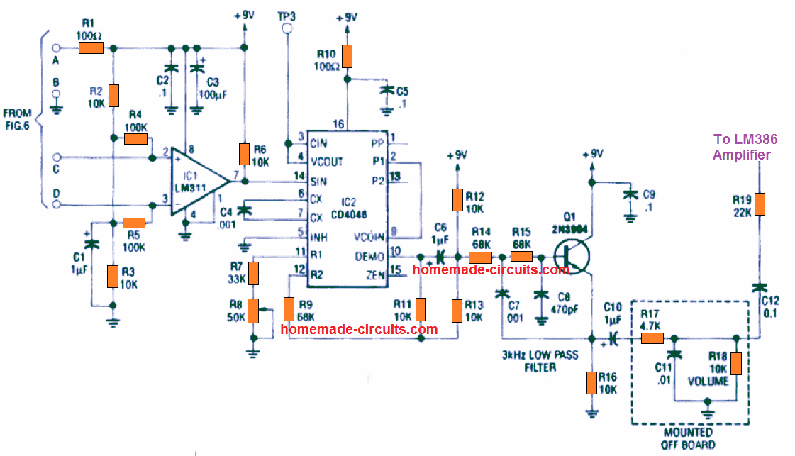
An LM311 comparator (IC1) switches the somewhat low analog signal to a digital signal for the CD4046 phase-locked loop (IC2). It must be noted that the amplitude of the retrieved acoustic signal is not relevant to the amplitude of the received signal. The amplitude of the retrieved audio is dependent only on the quantity of frequency deviation established by the transmitter and also the amplitude of the operator's voice.
The phase-locked loop (IC2) is set up like a first-order FM demodulator. Without applying any input signal, the center frequency of the network comprising IC2 pin 3 which is also TP3 is fine-tuned using R8 to set for a 50 kHz frequency.
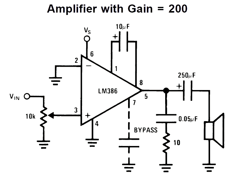
Due to the fact that the differences between the CD4046 brands could be quite significant, it may be necessary to modify R7 and, possibly, R9 also. The demodulated output through IC2 is filtered using a Q1 based 3 kHz low-pass filter. This signal is subsequently fed to audio power amplifier built using LM386 amplifier.

A larger bandwidth could be achieved by making the filter tp pass higher frequency. Since the "carrier" frequency is just 50 kHz, make sure not to expand the audio bandwidth to higher than 6 or 7 kHz.
PCB Designs


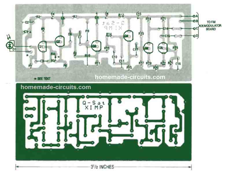

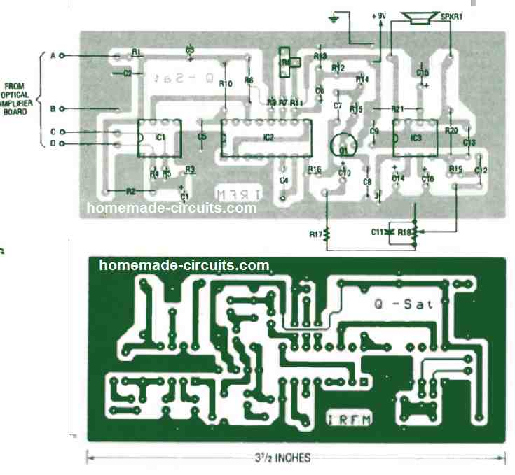
PLEASE NOTE THAT IN THE ABOVE PCB DESIGN, THE IC3 IS NOT AN LM386 BASED AMPLIFIER, RATHER SOME OTHER IC WHICH IS OBSOLETE NOW. PLEASE ADJUST THE AMPLIFIER SECTION WITH AN LM386 CIRCUIT BY REPLACING IC3 WITH LM386, AND BY SUITABLY ADJUSTING THE COMPONENTS AROUND IC3.

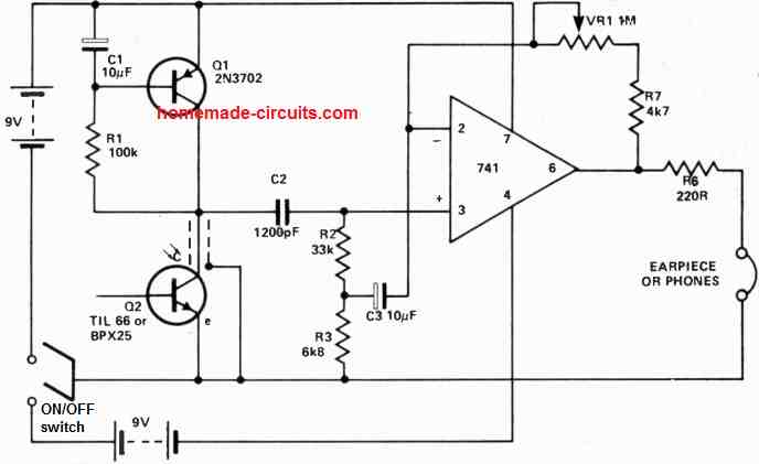
Another Optical Communicator Circuit
The optical transmitter circuit makes use of an LED to generate an AF controlled, infrared or visible stream of light which can be recognized by the phototransistor inside the receiver circuit. This phototransistor needs to have a peak sensitivity at the LED's peak emission wavelength in case the best possible efficiency is required. If the LED is in the form of infrared emitter TIXL26 producing nearly all of its radiation at 0.9um, then the phototransistor TIL66 becomes perfectly compatible with it.
On the other hand, visible red LEDs are also acceptable with this particular form of phototransistor, and each could be cheaper varieties compared to types recommended for an infrared sensitive system. Observe that the implementing infrared diode will not preclude the application of normal glass (borosilicate) lenses that are transparent to an emission of 0.9 um.
Observe that each of the shown circuits implements a standard op amp (the 741) like a sensitive preamplifier for detecting the audio signals from the microphone and the phototransistor. The circuits stages at the input side of the op amps work with a bootstrapping in order to boost the input impedance. In the transmitter circuit, a crystal microphone needs to be used. The earpiece spec is not crucial and it can have an impedance between 200 ohm to 2k ohm. The gain of the transmitter and the receiver circuits both is easily manipulated by allowing the feedback resistor (RV1) to be adjustable.
If you find the circuits behaving in an unstable manner during the operation, while examining the output signals, this could be corrected by hooking up a 470pF capacitor across the pins 6 and 2 of the op amp. The user may possibly think about enhancing the circuits to work through a single-ended supply. To implement this one can employ a voltage divider to increase the voltage on the noninverting pin to approximately fifty percent the supply voltage over which the signal voltage is impressed.
The theory of the optical light communication circuit can be witnessed in the circuit diagrams. In order to decrease the issues related to adjustments and aiming the signals, while you set up the circuits, at varying ranges from one another, the transmitter module must be adjusted to focus a parallel beam and the receiver must be appropriately adjusted to receive this beam.
This allows to achieve the collimation procedure by guaranteeing that the LED and phototransistor are focussed across the principal focus of the two lens. The lens diameters must be such as which enable taking the advantange fully of the radiation held inside the radiating cone of the LED.
In practical terms, a 50mm diameter and 150mm focal length lenses wold work in the most appropriate manner. Heavier lens having shorter focal length can be also tried which may allow the reduction of the lens diameter. However, in this situation the adjustment for collimation cold get more challenging due to the reducing focal length and to some extent because of the increased lens aberrations.
Transmitter Circuit

Receiver Circuit