In this post I have explained how to build NOT, AND, NAND, OR, and NOR logic gates using discrete transistors. The main advantage of using transistor logic gates is that they can work even with voltages as low as 1.5 V.
In some electronic applications the available voltage may be inadequate to power TTL or even CMOS ICs. This is especially true for gadgets that run on batteries. No doubt, you always have the 3-volt logic IC option. However, these are not always easily accessible to the enthusiast or experimenter, and they do not work below their defined voltage specifications (generally below 2.5 volts DC).
Furthermore, there might only be place for a single 1.5-volt battery in a battery-powered application. Well, then what are you going to do? Usually IC logic gates could be replaced by transistorized logic gates. For each particular logic gate, just a couple of transistors are generally required, and for a typical NOT gate inverter logic, just one transistor is required.
Advantages of Transistorized Logic Gates
- The main advantages of logic gates built using transistors can be summarized as given below:
- Transistors are cheaper than ICs.
- Transistorized logic gates can be operated with voltages as low as 1.5V, while the IC counterparts need a minimum of 3 V.
- A transistorized logic gate can be customized to control heavier loads, which an IC based logic gate cannot do.
FETs versus Bipolar Transistor
Field Effect Transistors (FETs) vs bipolar transistors: which is the better option for low-voltage transistorized logic circuits? One great feature of FETs is that their "on" resistance is incredibly low. Additionally, they need very low gate-turn-on current.
However, they have one limitation in extremely low-voltage applications. Typically, the gate voltage limit is one volt or so. Furthermore, the voltage available may decrease below the FET's optimum working range if a current-limiting or pull-down resistor is attached to the gate.
Conversely, bipolar switching transistors have an advantage in extremely low voltage, single battery applications since they only need 0.6 to 0.7 volts to switch on.
Furthermore, the majority of common FETs, which are normally sold in bubble packs at your nearest electronics store are often costlier than bipolar transistors. Also, a bulk packet of bipolar transistors could generally be purchased for the price of a pair of FETs.
FET handling necessitates significantly more care than bipolar transistor handling. Electrostatic and general experimental misuse make FETs particularly prone to damage. Burnt components may ruin an enjoyable, creative evening of experimentation or innovation, not to forget the emotional pain of debugging.
Basics of Switching Transistors
The logic circuit examples I have explained in this article make use of bipolar NPN transistors since they are affordable and don't need special handling. To avoid damaging the device or the parts that support it, suitable safety measures should be undertaken before connecting your circuit.
Even though our circuits are predominantly centered on Bipolar Junction Transistors (BJTs), they could have equally well been constructed using FET technology.
The basic switch circuit is a simple transistor application, which is one of the easiest designs.
Making a NOT Gate with a Single Transistor

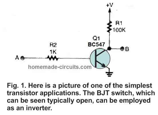
A schematic of the transistor switch is shown in Figure 1. Depending on how it is implemented in a particular application, the switch may be seen as either kept low or normally open.
A simple NOT gate inverter logic gate can be created by the straightforward switching circuit shown in Fig. 1 (where point A is the input). A NOT gate operates in such a way that if no DC bias is provided to the transistor's base (point A; Q1), it will remain shut-off, resulting in a high or logic 1 (equal to V+ level) at the output (point B).
However, the transistor activates when the proper bias is provided to the base of Q1, pushing the circuit's output low or to logic 0 (almost equal to zero potential). The transistor, designated Q1, is a general-purpose bipolar transistor, or a BC547, which is typically utilized in low-power switching and amplifier applications.
Any transistor that is equivalent to it (such the 2N2222, 2N4401, etc.) would work. R1 and R2's values were selected to strike a compromise between low current drain and compatibility. In all the designs, the resistors are all 1/4 watt, 5% units.
The supply voltage is adjustable between 1.4 and 6 volts DC. Note that the circuit can work like a buffer when the load resistor and output connection are shifted to the transistor's emitter.
Making a Buffer Gate using a Single BC547 BJT
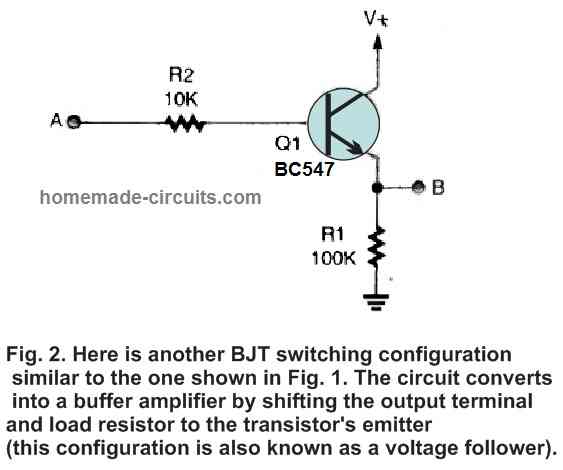
A voltage follower, or buffer amplifier, is a type of logic switching configuration identical to that shown in Figure 2. It should be noted that the load resistor and output terminal have been shifted from the transistor's collector to its emitter in this circuit, which is the primary difference between this design and the one shown in Fig. 1.
The transistor's functioning may also be "flipped" by moving the load resistor and output terminal to the other end of the BJT.
In other words, when no bias is provided to the circuit's input, the output of the circuit remains low; however, when a bias of adequate voltage is supplied to the circuit's input, the output of the circuit turns high. (That is exactly the opposite of what happens in the earlier circuit.)
Designing Two-Input Logic Gates using Transistors
AND Gate using Two Transistors
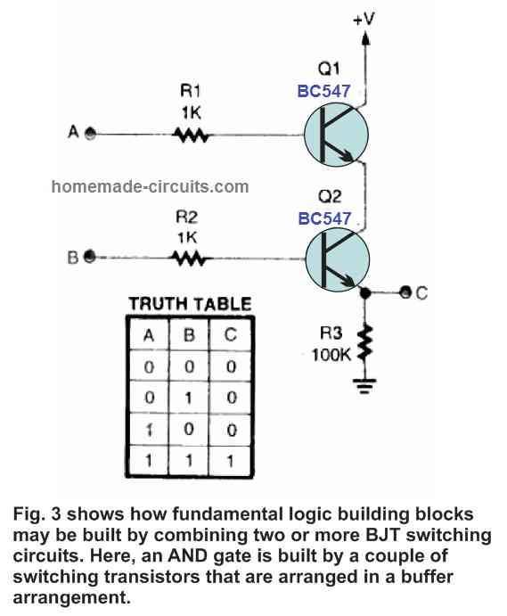
Figure 3 illustrates how a basic two-input AND gate may be created using a pair of buffers, along with the truth table for that gate. The truth table illustrates what the output results would be for each distinct set of inputs. Points A and B are used as the circuit's inputs, and point C serves as the circuit's output.
It is important to note from the truth table that just one set of input parameters results in a logic-high output signal, whereas all other input combinations result in a logic-low output. The output of the AND gate in Figure 3 remains slightly below V+ once it turns high.
This happens because of the voltage drop between the two transistors (Q1 and Q2).
NAND Gate using Two Transistors
Another variant of the circuit in Figure 3 and associated truth table are shown in Figure 4. The circuit turns into a NAND gate by shifting the output (point C) and output resistor to the upper transistor's (Q1) collector.
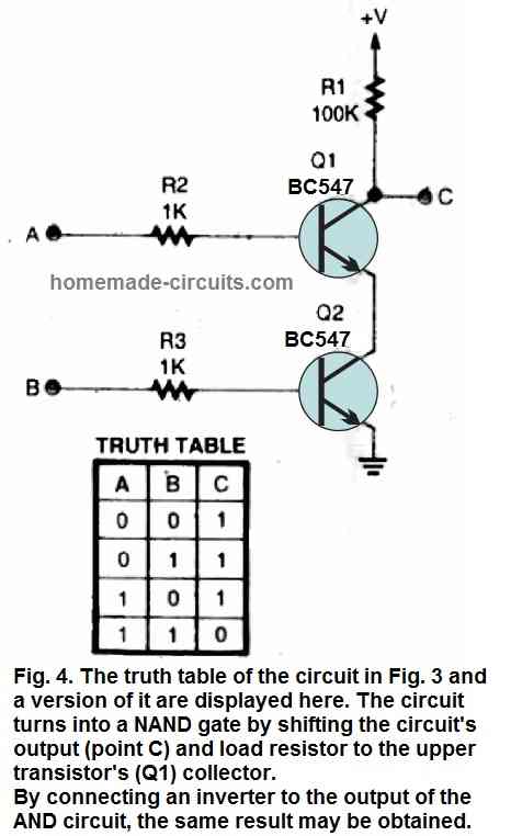
Since both Q1 and Q2 needs to be switched ON to pull the low side of R1 to ground, the voltage loss at output C is insignificant.
If the transistor AND or transistor NAND gates need more than two inputs, more transistors could well be connected in the shown designs to provide three, four, etc., input AND or NAND gates.
However, in order to compensate for the voltage losses of the individual transistors, V+ should be increased correspondingly.
OR Gate using Two Transistors
Another form of logic circuit with two inputs can be seen in Figure 5, along with the OR-gate circuit's truth table.
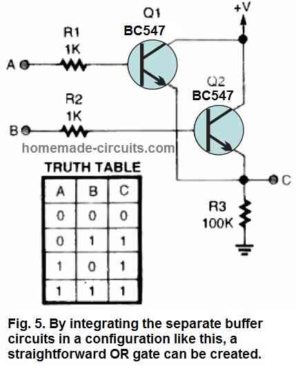
The output of the circuit is high when either input A or input B is pushed high, however due to the cascaded transistors, the voltage drop is over 0.5 volts. Yet again, the figures displayed indicate that there is enough voltage and current to operate the subsequent transistor gate.
NOR Gate using Two Transistors
Figure 6 depicts the next gate on our list, a two-input NOR gate, together with its truth table. Similar to how AND and NAND gates respond to one another, OR and NOR circuits do the same.
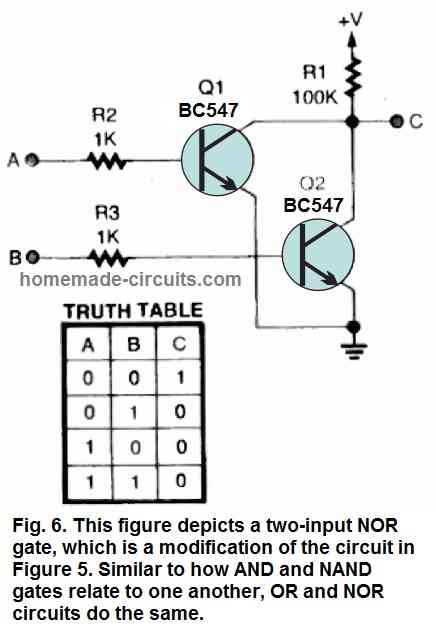
Each of the gates displayed is capable of supplying enough drive to activate at least one or more adjacent transistor gates.
Transistor Logic Gate Applications
What do you do with the above explained digital circuits that you now possess? Anything that you could accomplish with conventional TTL or CMOS gates, but without worrying about the supply voltage restrictions. Here are a few applications of transistor-logic gates in action.
Demultiplexer Circuit
A 1-of-2 demultiplexer with three NOT gates and two NAND circuits is seen in Figure 7. The appropriate output is chosen using the one-bit "address input," which may be either OUTPUT1 or OUTPUT2, while the driving information is applied to the circuit using the DATA input.
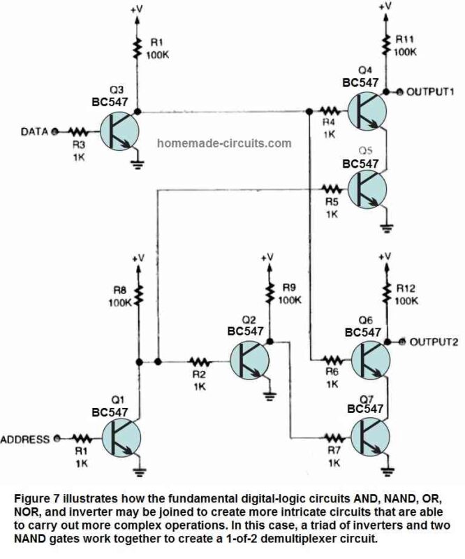
The circuit operates most effectively when the data rate is maintained under 10 kHz. The circuit's functionality is straightforward. The DATA input is supplied with the required signal, which turns Q3 ON and inverts the incoming data at Q3's collector.
The output of Q1 is driven high if the ADDRESS input is low (grounded or no signal is provided). At the Q1's collector, the high output is divided into two paths. In the first path, Q1's output is supplied to Q5's base (one of a two-input NAND gate's legs), turning it on and therefore "activating" the NAND gate made up of Q4 and Q5.
In the second path, Q1's high output is simultaneously supplied into the input of another NOT gate (Q2). After undergoing a double inversion, Q2's output turns low. This low is supplied Q7's base (one terminal of a second NAND gate, made up of Q6 and Q7), thus switching off the NAND circuit.
Any information or signal applied to the DATA input arrives at OUTPUT1 under these circumstances. Alternatively, the situation is reversed if a high signal is given to the ADDRESS input. Meaning, any information provided to the circuit will show at OUTPUT2 since the Q4/Q5 NAND gate is disabled and the Q6/Q7 NAND gate is enabled.
Oscillator Circuit (Clock Generator)
Our next transistor logic gate application, illustrated in Fig. 8, is a basic clock generator (also known as an oscillator) made out of three ordinary NOT gate inverters (one of which is biased using a feedback resistor, R2, which puts it into the analogue region).
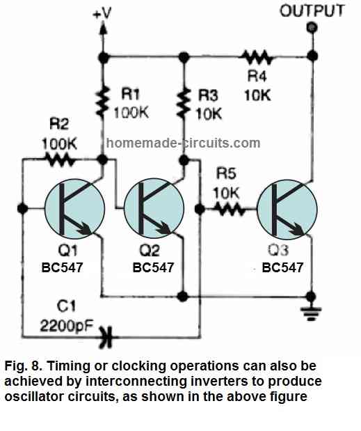
To square off the output, a third NOT gate (Q3) that delivers the complement to the oscillator output is included. The C1 value could be increased or decreased to change the circuit's operating frequency. The output waveform has a frequency of around 7 kHz with V+ at 1.5 volts DC, using the indicated component values.
RS Latch Circuit
Fig. 9 shows our final application circuit, an RS latch made up of two NOR gates. In order to ensure a healthy output drive at the Q and Q outputs, resistors R3 and R4 are adjusted to 1k ohms.
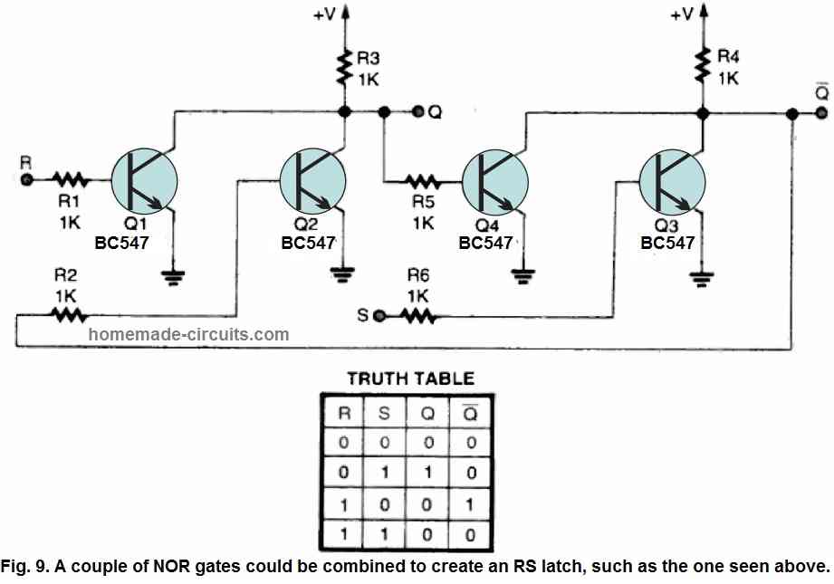
The RS latch's truth table is displayed alongside the schematic design. These are but a few illustrations of the several trustworthy, low-voltage, digital, logic-gate circuits that may be created using individual transistors.
Circuits Using Transistorized Logic Need Too Many Parts
Many issues can be solved using all of these low-voltage transistorized logic circuits. However, employing too many of these transistorized gates could lead to new issues.
The number of transistorizes and resistors might get fairly huge if the application you are building contains a large amount of gates, occupying valuable space.
Using transistor arrays (many transistors enclosed in plastic) and SIP (Single Inline Package) resistors in place of individual units is one way to solve this problem.
The above approach can save a tonne of space on a pcb while maintaining performance equal to that of their full-sized equivalents. Transistor arrays are offered in surface-mount, 14-pin through-hole, and quad pack packaging.
For most circuits, mixing transistor types may be quite acceptable.
Nevertheless, it is advisable that the experimenter works with a single type of transistor for building the transistorized logic circuits (meaning if you create a section of a gate using BC547, then try to use the same BJT for making the other remaining gates also).
The reasoning is that various transistor variants could have somewhat different properties and thus might behave differently.
For example, for some transistor the base switch-ON limit might be greater or smaller than another, or one could have an overall current gain that is a bit higher or lower.
On the other hand, the cost of buying a bulk box of a single type of transistor could be also lower. The performance of your circuits will enhance if your logic gates are built using matching transistors, and the project in its entirety will be more rewarding ultimately.

Have Questions? Please Leave a Comment. I have answered over 50,000. Kindly ensure the comments are related to the above topic.
What are components that required for this exp
नमस्ते, can I use 5 volt supply instead of the 12v in your diagram
Yes, you can use any voltage between 3V and 12V.
Thank you very much help….Namaste
नमस्ते, I just posted a query.. Please note the mistake I made… I mentioned micro switch… It should read Slow Vibration Sensor Switch (Hard to trigger)…. Thanks
Hi, you can use the following circuit: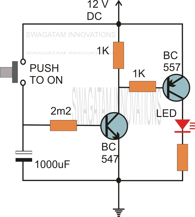
Replace the push button with your vibration source.
Replace 2.2M with 1k resistor
Remove the 1000uF capacitor, it is not required.
Replace the LED with a short, replace LED resistor with 1M resistor.
Feed the collector of the BC557 to the input of the NOT gate.
नमस्ते, thank you for your quick response.. I’ll try out this circuit and provide feedback…
Sure, thanks.
I want to know the inner knowledge how we are arranging transistors in order to prepare a new gate
Please see how the transistors are switched ON in response to their base signals. This is how the transistors are configured to replicate CMOS gates
Hi, thanks please example in practical logic gatecircuit
The examples are given at the end of the post!