In this post I have explained how to build simple oscillator circuits like the pierce oscillator and hartley oscillator using a single CMOS gate. Both the oscillators are types of oscillators that utilize minimum number of components yet are able to generate very stable and reliable frequency outputs.
You might also want to learn How to Build a Colpitts Oscillator
Pierce Oscillator
You can easily build a pierce oscillator circuit, based on a crystal oscillator design, using a single CMOS gate, as shown in the following figure.

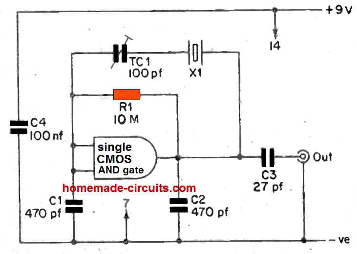
The single CMOS inverter is biased to form a linear amplifier by means of R1. A crystal can be seen connected between the input and the output of the pierce circuit through the trimmer capacitor TCI.
This proposed circuit is designed to operate with the series resonant frequency of the crystal. Needless to say, a positive feedback hasn't been used here between the output and input of the circuit. This is because, the CMOS amplifier's input and output work in the antiphase mode.
With series resonance it might look as if the crystal is supplying the negative feedback to the amplifier. However, this might not be true in reality, because C1 and C2 create a capactive centre tap around the crystal, where the centre tap can be seen grounded.
The crystal as a result behaves like a form of transformer working in the series resonance mode, using its a pair of connections operating in antiphase. Consequently, we may find a 180 degree phase shift by means of the two amplifier and the crystal, and also with a positive feedback.
TC1 is included to tailor the circuit's oscillation frequency to match the crystal's nominal frequency, but anyway, this specific function could be omitted in case it is not required. TC1 can now be removed and the crystal can be hooked up directly across R1.
Capacitors C1 and C2 can be seen having the values of 470 pF each in this pierce circuit design. With these values the circuit must oscillate without any problems within a extensive range of frequencies. If the frequency is just a few MHz then you may want to decrease the value of C1 and C2 relatively so that you can sustain the oscillation correctly. Alternatively, when the frequencies is lower than a few 100 kHz you can select C1 and C2 values a little bit larger.
An AND CMOS gate is indicated in the diagram, it is also possible to use a buffer CMOS gate, such as from the IC 4050.
Using an FET
A benefit of the Pierce crystal oscillator circuit is that it does not require any tuning adjustments. The following figure demonstrates how to build a Pierce oscillator circuit using a single 2N3823 (or 2N3821, 2N3822) field-effect transistor.
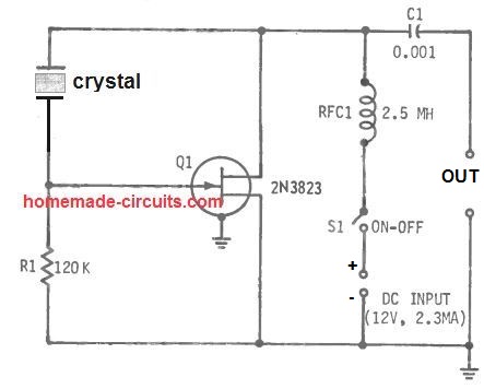
In this set up, the quartz crystal (XTAL) is driven between the FET's drain/output and gate/input stages. The 2.5-mh RF choke (RFC1) doesn't typically tune the circuit, however it assists just to keep the RF energy away from the DC supply. The circuit starts oscillating the moment switch S1 is switched ON.
Capacitive output coupling is supplied by means of the capacitor C1, which ensures that that the external load impedance be high enough so that it does not overload the circuit and destroy the oscillations. During the time the pierce oscillator circuit oscillates at the crystal frequency, it comsumes around 2.3 ma current from the 12 V DC supply.
At this time, without any load the RF output signal amplitude is 6.2v RMS (in the shown circuit this was implemented at 7 MHz frequency).
The Pierce circuit is designed to oscillate at the fundamental frequency of the crystal. Hence, in case there is a harmonic-type crystal, oscillation will happen in the primary frequency of the crystal, not necessarily in the specified (harmonic) frequency. Additionally, the Pierce oscillator requires an extremely active crystal.
Another Single FET Pierce Oscillator Circuit
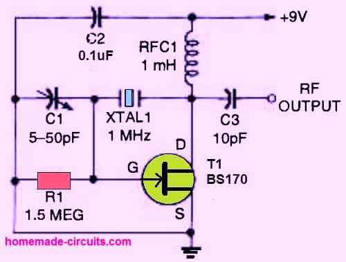
Another straightforward Pierce crystal-controlled oscillator circuit is depicted in the above image. This circuit could be implemented as a marker generator for receiver aligning purposes.
The active element generating enough gain for the circuit to oscillate is a single FET (field-effect transistor) BS170. The input gate receives feedback from the FET's drain (d) through the crystal. The oscillator is fine-tuned by the trimmer capacitor C1.
Hartley Oscillator
The Hartley oscillator is a type of frequency generator circuit in which the oscillation frequency depends upon a tuned circuit which involves capacitors and inductors, meaning, it is simply a type of an LC oscillator.
A single CMOS inverter can be also used to build the popular Hartley type oscillator. This type of Hartley oscillator circuit is more advantageous than normal LC oscillators, since here just just one winding is necessary for the coil. Even so, the coil needs to be a center tapped winding. The CMOS Hartley oscillator circuit diagram can be visualized in the following figure.
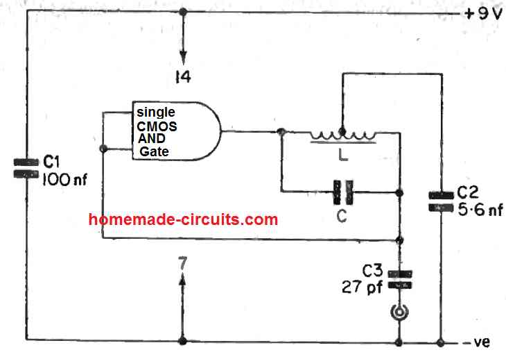
The working of the ahrtley oscillator is quite similar to the pierce oscillator, except the use of the a center tapped LC stage which is used instead of the capactively center tapped crystal.
The inductor L supplies a D.C. route between the CMOS inverter's input and output which ensures that the circuit can work without the need of a bias resistor.
The circuit can work with with a frequency range of a several 100 kHz but below a maximum of 10 MHz. These frequencies will depend on the values of the L and C which must appropriately selected to match the specified operating frequency range.
You can make the capacitor C variable, in case you want the Hartley circuit to work like a variable frequency oscillator. Remember that the indicated tapping on the coil L doesn't need to be at exactly at the middle of the winding, which means for example, the circuit may run without any issues even with the primary of an I.F. transformer used in place of L.
The coil L can be experimented by using different number of turns over a ferrite core, and testing the results over a frequency meter.
An AND CMOS gate has been used in the hartley diagram, you can also likewise use a buffer CMOS gate, such as from the IC 4050.
Using a single Transistor
A type of oscillator single transistor circuit that is tuned with a transformer and generates a sine wave AF, can be witnessed in the following figure. This is actually a Hartley type oscillator circuit, where the tuning and feedback features are achieved through just one center-tapped winding of the transformer; the other winding of the transformer subsequently works like as an output coupling coil.
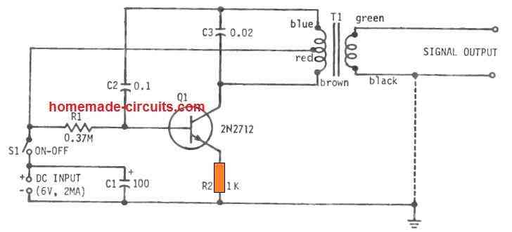
To build this Hartley circuit, you must first procure the small transformer T1 which is a 500 ohm to 30 ohm center tapped transformer. Meaning the circuit winding has 500 ohm and the output side winding has 30 ohm approximately.
The upper half section of the center-tapped primary winding of L1 acts like the base-input coil while the bottom half of the primary side of L1 act s like the collector output coil.
Capacitor C3 solely becomes responsible for tuning the oscillation on the primary side of the transformer. The frequency of the Hartley circuit is mainly established by capacitor C3 and the inductance of the total primary winding.
As indicated in the diagram if C3 value is 0.02 mfd, then the frequency will be roughly around 2 kHz. In order to raise the frequency, you may try lowering the C3 capacitance; to decrease the frequency simply increase the C3 capacitance.
To ensure that the circuit oscillates perfectly, the transformer winding should be correctly polarized as provided in the specs of the transformer by color dots.
Capacitor C2 does not have any role in the tuned circuit, yet it is positioned to prohibit the collector DC voltage appearing from the base of the transistor. The circuit provides an amplitude of 0.8 V RMS when the output is not loaded. The current consumption is 2 ma when a 6V Dc supply is used for the circuit
Hartley Oscillator with LC Feedback
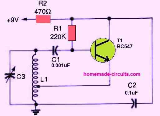
The figure above displays a contemporary RF Hartley transistor oscillator circuit. The values of L1 and C3 control the oscillator's working frequency. The placement of the tap on L1, which is typically between 1/5th and 1/4th of the total turns, determines the feed-back level.
This Hartley oscillator, for instance, will run at 5 MHz if the L/C combinations are as follows. L1 consisting of 20 turns of 18 SWG enameled copper wire, tightly wound over a 1 -inch plastic former. It has a tapping after five turns from the bottom.
C3 is a tiny adjustable capacitor which may have a highest capacitance value of 100 pF. The Hartley oscillator is a particularly well-liked circuit among circuit designers since it can function in the low audio range to UHF range with the appropriate L/C values.
Need Help? Please Leave a Comment! We value your input—Kindly keep it relevant to the above topic!