MOSFET based amplifiers as we all know are outstanding with their sound qualities and they can easily beat the performance of other counterparts based on power transistors or linear ICs.
Why use MOSFETs in Amplifiers
Amplifiers based on mosfets are not always easy to design or make.
Moreover after assembling a prototype, testing to perfection always remains an issue with new electronic hobbyists.
You might have come across many hi-fi complex mosfet amplifier designs, but might have not dared making it just because of the above reasons.
The simple mosfet amplifier circuit diagram is super simple to build and yet will provide you with a crystal clear 100 watts of raw music power that all the listeners will cherish for a long time.
The idea was developed a long time ago by the Hitachi researchers and still it remains one of the favorite designs of all time considering the involved simplicity against quality.
How the Amplifier is designed to Function
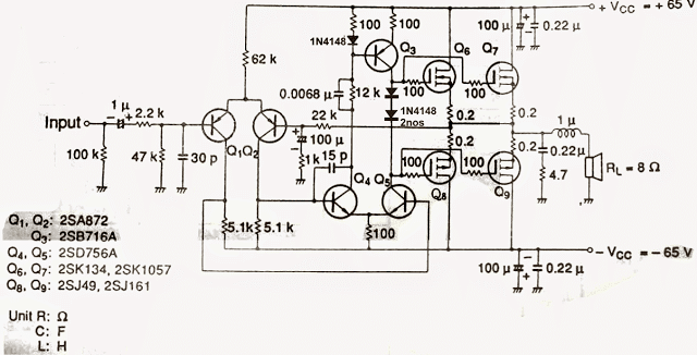
Looking at the figure we can understand the circuit with the following points:
- The involved simplicity would also certainly mean that some of the ideal features of the circuit was sacrificed in the design, for example it lacks a constant current source for the differential amplifier at the input stage of the amplifier.
- But this has no serious impact on the design, whatsoever..
- The differential amplifier makes sure that the input is sufficiently amplified to some reasonable levels suitable for feeding the next driver stage.
- The driver stage consists of a well balanced high voltage transistor stage which are necessarily positioned for driving the output power mosfets.
- The pot positioned in between the two sections of the driver stage is used for setting the quiescent current of the circuit.
- The output stage is a common push pull type of mosfet stage which finally provides the boost for amplifying the fed low signal music into a 100 watt thumping music over a 8 Ohm speaker.
- The shown parts might be obsolete today so may be replaced as follows:
- The differential transistor may be replaced with BC556.
- The driver transistors may be replaced with MJE350/MJE340.
- The mosfets may be replaced with 2SJ162/2SK1058
The below given diagram is the original design from Hitachi, see the preset arrangement for setting up the quiescent current. You must adjust this preset to set the quiescent current to zero before connecting the speaker.
I have modified the above design by adding a couple of 1N4148 diodes in place of the preset. This gets rid of the preset adjustments and allows the user to directly switch ON the amp with a speaker connected.
Parts List
Resistors
All resistors are 1/4 watt, CFR 5%, unless otherwise stated.
- 100 Ohm = 7nos
- 100k = 1no
- 47k = 1no
- 5.1k = 2nos
- 62k = 1no
- 22k = 1no
- 2.2k = 1no
- 12k = 1no
- 1k = 1no
- 4.7 ohm = 1no
- 0.2 ohm / 5 watts = 4nos
Capacitors
All capacitors must be minimum 100V rated
- 1uF = 1no Electrolytic
- 100uF = 3nos Electrolytic
- 15pF = 1no Polyester
- 30pF = 1no Polyester
- 0.22uF = 3nos Polyester
- 0.0068uF = 1no Polyester
Semiconductors
- Q1, Q2 = BC546
- Q3 = MJE350
- Q4, Q5 = MJE340
- Q6, Q7 = 2SK1058
- Q8, Q9 = 2SJ162
- 1N4148 = 2nos
Misc
Inductor = 1uH, 20 turns of close wound 1mm super enameled copper wire, with 10mm diameter (air core)
Note: The resistor, and capacitor values are not critical, slight up and down will do, and will not cause any harm to the performance of the amplifier
Parts, PCB Images and Prototype
1) The first image shows the PCB which was used for the 100 watt mosfet amplifier circuit project
2) The second pic shows the soldered portion of the assembled circuit.
3) The third pic illustrates the components side of the assembled board
4) The fourth image relates with a few of the components involved with the the circuit making.
5) The fifth figure witnesses the speakers which was used for testing the amplifier with astonishing levels of clarity and superb power outputs :p
I used only a couple of mosfets which could generate power outputs well over 100 watts RMS, connecting more numbers in parallel can easily enable this circuit to cross beyond the 1000 watts mark.
If you are intending to buy a ready made power amplifier for your home, I would suggest, you build this one instead and be the proud owner of this outstanding home built power amplifier unit which would probably serve you for years.
The Design which I Built
The circuit which I tested was taken from eeweb, and the diagram is shown below. It is similar to the above original design from Hitachi. However since this is the one which I have tested I would recommend you to go with this one.
Circuit Diagram with Magnified Part Values
PCB Track, and Component Layout Diagrams
Credit to the Original Creator
PCB Dimensions are 120 mm x 78 mm

