In this post I have explained how to make a simple variable power supply circuit using transistor 2N3055 and some other passive components. It includes variable voltage and variable current feature, fully adjustable.
Main Specifications
1) Adjustable from 0-30V, 0-60V, and 0-100V, and 500mA to 10 Amp as per user preference
2) Short Circuit Protected when mounted on proper heatsink
3) Ripple free, with less than 1Vpp
4) Output is Stabilized and filtered DC
5) Short circuit LED indicator
6) Overload Protected
Introduction
A power supply circuit that does not include the features of a variable voltage and current control can by no means be considered truly versatile.
A variable workbench power supply circuit I have explained in this article is not only specified with a continuously variable voltage control but is also equipped with the feature of overload or continuously variable current control.
Circuit Diagram

How it Works
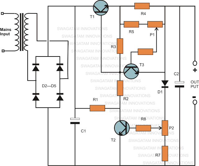
A keen look at this 2N3055 based variable voltage current power supply circuit using transistor 2N3055 reveals that it’s actually only an ordinary stabilized power supply circuit, however it yet still provides you with the proposed features very efficiently.The voltage variations are made by using the preset P2, through a feedback configuration employing the components D1, R7, T2 and P2.
The inclusion of D1 makes it sure that the voltage can be lowered right down to 0.6 volts, which happens to be the forward voltage drop of the diode.
If any other specific minimum value is required then the diode can be replaced by zener diode having the required specified value.
Therefore in this variable power supply circuit using 2N3055 transistor, the transformer being a 0 – 40 V, the output becomes variable right from 0.6 to 40 volts maximum, that’s very handy indeed.
For implementing the current control feature, T3 along with P1, R5 and R4 are involved.
The value of R4 is specifically becomes responsible for defining the maximum allowable output current.
P1 is set to choose the maximum range within the value that’s marked or identified by the resistor R4.
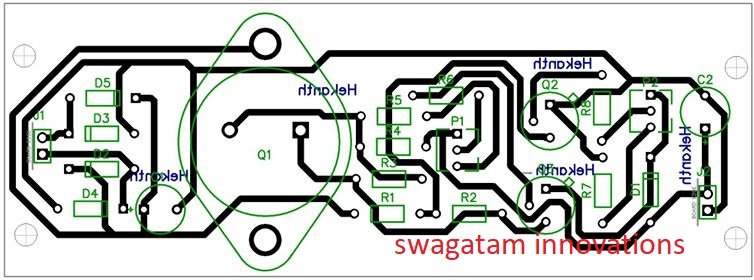
PCB Design
Parts List
- R1 = 1K, 5 watt wire wound
- R2 = 120 Ohms,
- R3 = 330 Ohms,
- R4 = to be calculated using Ohms law.
- R5 = 1K5,
- R6 = 5K6,
- R7 = 56 Ohms,
- R8 = 2K2, P1,P2 = 2k5 presets
- T1 = 2N3055,
- T2, T3 = BC547B,
- D1 = 1N4007,
- D2, D3, D4, D5 = 1N5402,
- C1, C2 = 1000uF/50V,
- Tr1 = 0 – 40 Volts, 3 Amp
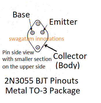
2N3055 Pinout Details
If you have any doubts regarding this variable voltage and current power supply circuit using transistor 2N3055 circuit please do not hesitate to ask then through the comments below.
Original Transistor Power Supply Diagram:
The above design was inspired from the following circuit which was designed and presented in the elektor electronics magazine by the elektor engineers:
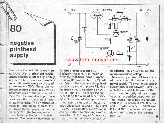
Simplified Variable Power Supply Design using 2N3055 and 2N2222 Transistors
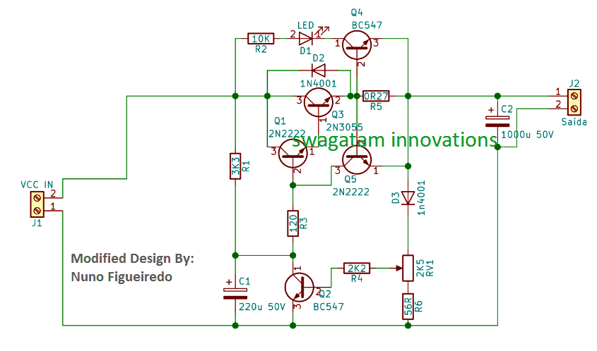
The above designs were assessed and simplified with more effective results by Mr. Nuno. The revised and simplified design can be viewed in the following diagram:
The design features an over-current shut down with LED indication.
Video clip of the tested prototype:

For PCB Design and other Related Data, you can Download the following ZIP File:
PCB Design for the above Circuit
Another Similar Power Supply Design as Referred by Mr. William C. Colvin is presented below for the viewer assessment:
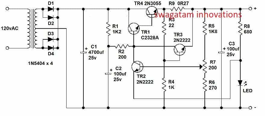
2N3055 Wide Range Variable Voltage Regulator
The key highlights of the circuit are: wide range output: 0.1 to 50 volts excellent load regulation: 0.005% between 0 and 1 amp, decent line regulation: 0.01%, reduced output disturbance: superior to 250 microvolts.
The broad output selection is implemented with thehelp of the integrated circuit CA 3130, that is able to work even with a zero volt input/output differential. In addition, higher extension of the output range becomes feasible through the inclusion of T4 between the IC and the series pass transistor.
The high gain as a result acquired enables a superior level of regulation, and the T1/T2 Darlington pair offers a adequately large current boosting. T3 works like an output current controller.
When P1 is rotated totally anti-clockwise, T3 restricts at 0.6 amps. The limiting circuit becomes inactive when P2 is moved completely clockwise. The regulator circuit specifically operates in the following manner.
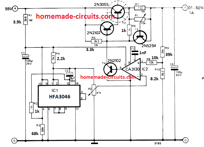
The IC CA 3130 analyzes the output voltage given to the non-inverting input with respect to a reference voltage at the inverting input.
The output voltage of the regulator is reduced with a potential divider to protect against damage to the IC.
The reference voltage is determined by P2, which needs to be a top-notch part, since any kind of noise upon its slider arm will probably be transferred to the regulator output terminals.
A additional IC, HFA3046 , offsets the reference voltage intended for temperature variations. The IC is made up of 4 transistors applied as diodes or zener and another transistor for cutting down the output impedance of the reference circuit.
The reference IC furthermore provides a stepped down supply voltage for powering CA 3130. This feature necessitates the use of each ICs in the regulator stage; if IC1 is removed can result in the break down of IC2. Each of the transistors shown in the diagram must be rated with a breakdown voltage of a minimum of 55 volts.
High Current Variable Power Supply
In this high current linear power supply circuit, we have used a 2N5686 transistor instead of 2N3055, so that the circuit is able to deliver a minimum of 10 amp current, and the preset P3 could be used to adjust a current range of 10 amp.
The power supply itself is pretty straightforward to construct. An IC LM329 provides a steady reference voltage of 6.9 V.
P4 is a potentiometer, and this pot is utilized to determine the output voltage using a preset potential divider P2-P4-R2. The power stage of the circuit is made up of IC1 and T1, which operate like an operational amplifier when it comes to positive voltages (negative voltages are not relevant here, obviously).
This non-inverting amplifier is built using an combo of op amp, P1, R5, and R6. This indicates that the voltage at P4's wiper is proportionate to the voltage across the output terminals.
P1 is a potentiometer that controls the peak output voltage, while P2 is used for setting the minimum output voltage from the power supply.
Preset P3 is used for setting up the maximum current limit of the output.
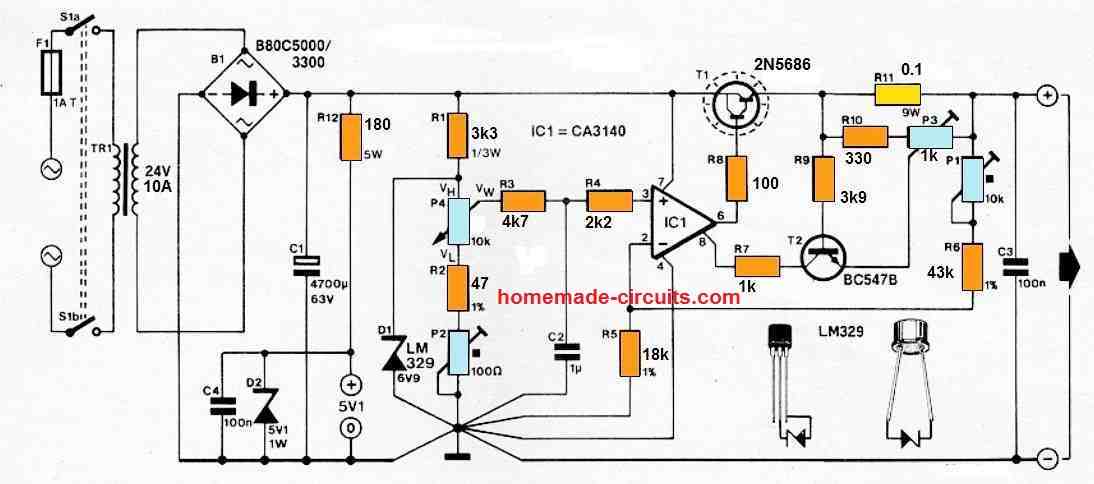
R11 converts the output current to a voltage to accomplish this. When this voltage (controlled by P3) is large enough to turn on T2, the circuit's voltage regulation is superseded by current regulation through IC1's strobe input. The maximum current that can be adjusted is from 0.8 A to 10 A, depending on how the controls are adjusted.
When the output of the power supply are short-circuited, the current must not increase above 25 A to prevent T1 from being damaged and due to over dissipation. The circuit setting up is not complicated. To begin, adjust P4 to highest possible resistance and wait about a minute until Z1 and IC1 reach their typical working temperatures. Next, adjust P1 to get a 25 V output voltage.
Finally, tweak P2 to provide a 250 mV output voltage by setting P4 to lowest resistance. The lowest output voltage of 250 mV was selected on purpose to guarantee that the individual parts always are able to work with a linear region of their characteristics. There are a couple of things to remember here: the earth lines must be routed exactly as shown in the schematic, and T1 must be installed on a 1.5 K/ W heat sink.
