

If you have understood correctly, how to use transistors in circuits, you might have already conquered half of electronics and its principles. In this post we make an effort in this direction.
Introduction
Transistors are 3 terminal semiconductor devices which is able to conduct relatively high power across their two terminals, in response to a significantly low power input at the third terminal.
Transistors are basically of two types: bipolar junction transistor (BJT), and metal–oxide–semiconductor field-effect transistor (MOSFET)
For a BJT, the 3 terminals are designated as base, emitter, collector. A low power signal across base/emitter terminal allows the transistor to switch a comparatively high power load across its collector terminal.
For MOSFETs these are designated as Gate, Source, Drain. A low power signal across Gate/Source terminal allows the transistor to switch a comparatively high power load across its collector terminal.
For the sake of simplicity we will discuss BJTs here, since their charcaeritics is less complex compared to MOSFETs.
Transistors (BJTs) are the building blocks of all semiconductor devices found today. If there wouldn’t be transistors there wouldn’t be any ICs or any other semiconductor component. Even ICs are made up of 1000s of closely knit transistors which constitute the features of the particular chip.
New electronic hobbyists usually find it difficult to handle these useful components and configure them as circuits for an intended application.
Here we’ll study the functions and the way of handling and implementing bipolar transistors into practical circuits.
How to use Transistors like a Switch
Bipolar transistors are generally a three lead active electronic component which fundamentally work as a switch for either switching ON or switching OFF power to an external load or an associated electronic stage of the circuit.
A classic example can be seen below, where a transistor is connected as a common emitter amplifier:


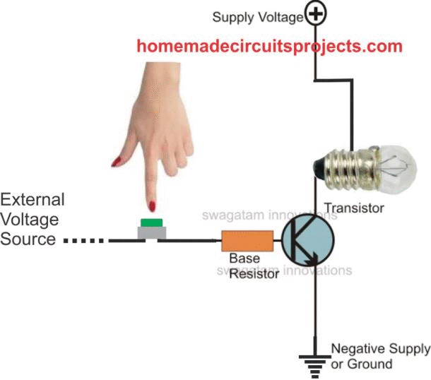
This is the standard method of using any transistor like a switch for controlling a given load. You can see when a small external voltage is applied to the base, the transistor switches ON and conducts heavier current across the collector emitter terminals, switching on a bigger load.
The base resistor value can be calculated using the formula:
Rb = (Base Supply Vb - Base-Emitter Forward Voltage) x hFE / Load Current
Also remember that, the negative or the ground line of the external voltage must be connected with the transistor ground line or the emitter, otherwise the external voltage will have no effect on the transistor.
Using Transistor as a Relay Driver
I have already explained in one of my earlier posts regarding how to make a transistor driver circuit.
Basically it uses the same configuration as shown above. Here's the standard circuit for the same:
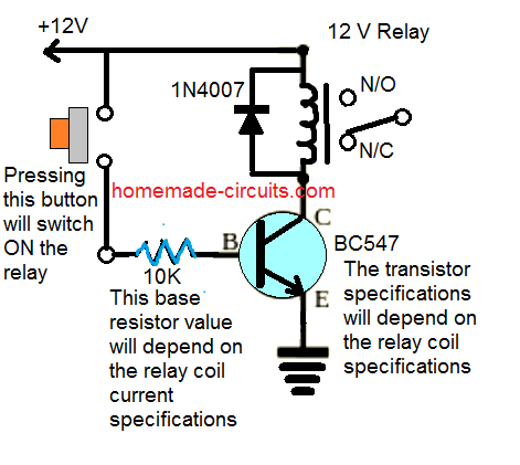
If you are confused about the relay, you can refer to this comprehensive article which explains everything about relay configurations.
Using Transistor to Light Dimmer
The following configuration shows how a transistor can be used as a light dimmer using a emitter follower circuit.
You can see as the variable resistor or the pot is varied, the lamp intensity also varies. We call it emitter-follower, because the voltage at the emitter or across the bulb follows the voltage at the base of the transistor.
To be precise the emitter voltage will be just 0.7 V behind the base voltage. For example, if the base voltage is 6 V, the emitter will 6 - 0.7 = 5.3 V and so on. The 0.7 V difference is due to the minimum forward voltage drop rating of the transistor across the base emitter.

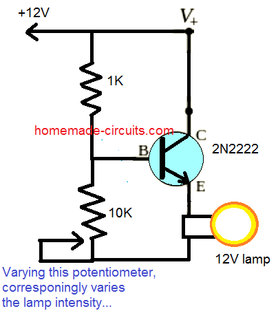
Here, the pot resistance along with the 1 K resistor forms a resistive divider network at the base of the transistor. As the pot slider is moved, the voltage at the base of the transistor is changed, and this correspondingly alters the emitter voltage across the lamp, and the lamp intensity changes accordingly.
Using Transistor as a Sensor
From the above discussions you might have observed that the transistor is doing one crucial thing in all the applications. It is basically amplifying the voltage at its base by allowing a large current to be switched across its collector emitter.
This amplifying feature is also exploited when a transistor is used as a sensor. The following example shows how it can used to sense the difference in ambient light, and switch ON/OFF a relay accordingly.

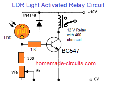
Here too the LDR and the 300 ohm/5 k preset forms a potential divider at the base of the transistor.
The 300 ohm is actually not required. It is included to ensure that the transistor base is never fully grounded, and thus it is never completely disabled or shut off. It also ensures that the current through the LDR can never exceed a certain minimum limit, no matter how bright the light intensity is on the LDR.
When it's dark, the LDR has a high resistance which is many times higher than the combined value of the 300 ohm and the 5 K preset.
Due to this the transistor base gets more ground side voltage (negative) than the positive voltage, and its collector/emitter conduction remains switched OFF.
However when sufficient light falls on the LDR, its resistance drops to a few kilo-ohm value.
This enables the base voltage of the transistor to rise well over the 0.7 V mark. The transistor now gets biased and switches ON the collector load, that is the relay.
As you can see, in this application too the transistors is basically amplifying the tiny base voltage such that a bigger load at its collector could be switched ON.
The LDR can be replaced with other sensors such as a thermistor for heat sensing, a water sensor for water sensing, a photodiode for IR beam sensing, and so forth.
Question for you: What happens if the position of the LDR and the 300/5 K preset are swapped with each other?
Transistor Packages
Transistors are normally recognized by their external package in which the particular device may be embedded. The most common types of package in which these useful devices are enclosed, are the T0-92, TO-126, TO-220 and TO-3. We will try to understand all these specifications of transistors and also learn how to use them in practical circuits.
Understanding Small Signal TO-92 Transistors:
Transistors like BC547, BC557, BC546, BC548, BC549, etc all come under this category.
These are the most elementary in the group and are used for applications involving low voltages and currents. Interestingly this category of transistors is used most extensively and universally in electronic circuits due to their versatile parameters.

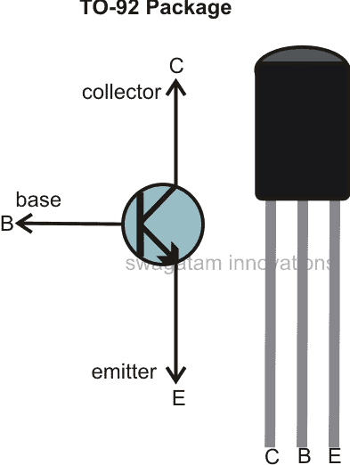
Normally these devices are designed to handle voltages anywhere between 30 to 60 volts across their collector and emitter.
The base voltage is not more than 6, but they can be easily triggered with a voltage level as low as 0.7 volts at their base. However the current must be limited to 3 mA approximately.
The three leads of a TO-92 transistor may be identified in the following manner:
Keeping the printed side toward us, the right side lead is the emitter, the center one is the base and the left hand side leg is the collector of the device.
UPDATE: Want to know how to use transistors with Arduino? Read it here
How to Configure a TO-92 Transistor into Practical The Designs
Transistors are mainly of two types, an NPN type and a PNP type, both are complementary to each other. Basically they both behave the same way but in the opposite references and directions.
For example an NPN device will require a positive trigger with respect to the ground while a PNP device will require a negative trigger with reference to a positive supply line for implementing the specified results.
The three leads of the transistor explained above needs to be assigned with specified inputs and outputs for making it work for a particular application which obviously is for switching a parameter.
The leads need to be assigned with the following input and output parameters:
The emitter of any transistor is the reference pinout of the device, meaning it needs to be assigned the specified common supply reference so that the remaining two leads can operate with reference to it.
An NPN transistor will always need a negative supply as the reference, connected at its emitter lead for proper functioning, while for a PNP, it will be the positive supply line for its emitter.
The collector is the load carrying lead of a transistor and the load which needs to be switched is introduced at the collector of a transistor (see figure).

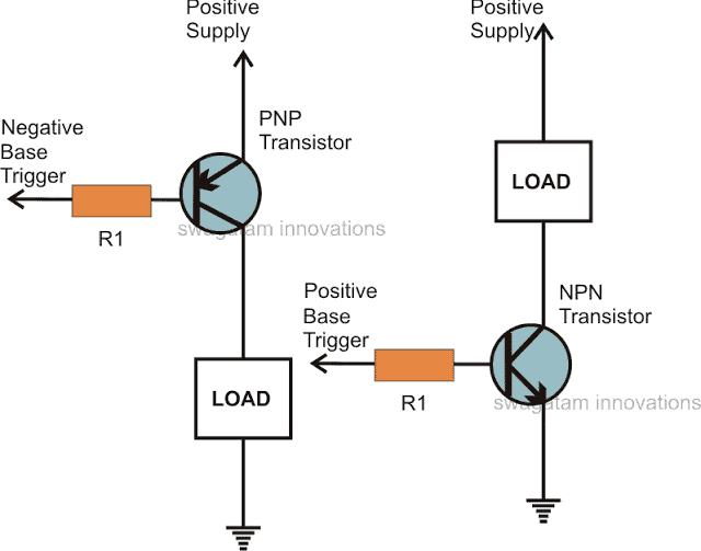
The base of a transistor is the trigger terminal which is required to be applied with a small voltage level so the current through the load can pass through, across to the emitter line making the circuit complete and operating the load.
The removal of the trigger supply to the base immediately switches OFF the load or simply the current across the collector and the emitter terminals.
Understanding TO-126, TO-220 Power Transistors:
These are medium type of power transistors used for applications which require switching of powerful relatively powerful loads lie transformers, lamps etc. and for driving TO-3 devices, typical egs are BD139, BD140, BD135 etc.

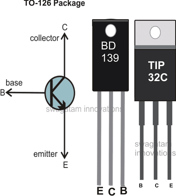
Identifying BJT pinouts
The pinout are identified in the following manner:
Holding the device with its printed surface facing you, the right side lead is the emitter, the center lead is the collector and the left side lead is the base.
The functioning and the triggering principle is exactly similar to what is explained in the previous section.
The device is operated with loads anywhere from 100 mA to 2 amps across their collector to emitter.
The base trigger can be anywhere from 1 to 5 volts with currents not exceeding 50 mA depending upon the power of the loads to be switched.
Understanding TO-3 Power Transistors:
These can be seen in metallic packages as shown in the figure. The common examples of TO-3 power transistors are 2N3055, AD149, BU205, etc.

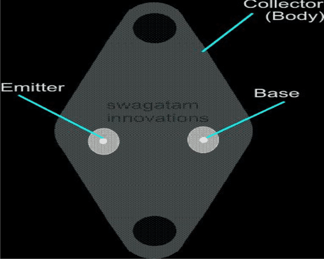
The leads of a TO-3 package can be identified as follows:
Holding the lead side of the device toward you such that the metal part beside the leads having larger area is held upward (see figure), the right side lead is the base, the left side lead is the emitter while the metallic body of the device forms the collector of the package.
The function and operating principle is just about the same as explained for the small signal transistor however the power specs increase proportionately as given below:
Collector-emitter voltage can be anywhere between 30 to 400 volts and current between 10 to 30 Amps.
Base trigger should be optimally around 5 volts, with current levels from 10 to 50 mA depending upon the magnitude of the load to be triggered. The base triggering current is directly proportional to the load current.
Have more specific questions? Please ask them through your comments, I am here to solve them all for you.