The IC 4017 can be considered as one of the most useful and versatile chip having numerous electronic circuit applications.
About IC 4017
Technically it is called the Johnsons 10 stage decade counter divider. The name suggest two things, it’s something to do with number 10 and counting/dividing.
The number 10 is connected with the number of outputs this IC has, and these outputs become high in sequence in response to every high clock pulse applied at its input clock pin out.
It means, all its 10 outputs will go through one cycle of high output sequencing from start to finish in response to 10 clocks received at its input (pin#14). So in a way it is counting and also dividing the input clock by 10 and hence the name.

Understanding pinout Function of IC 4017
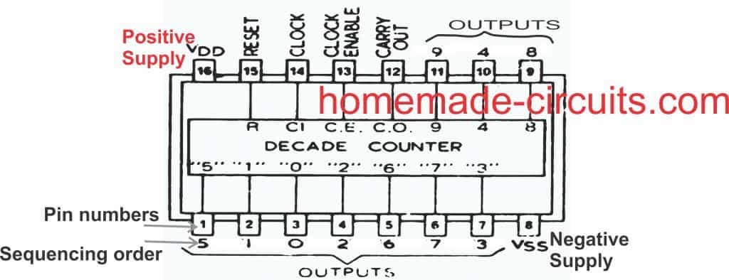
Let’s understand the pin outs of the IC 4017 in details and from a newcomer’s point of view: Looking at the figure we see that the device is a 16 pin DIL IC, the pin out numbers are indicated in the diagram with their corresponding assignment names.
What do Logic High, Logic Low Mean
The pinout which are marked as outputs are the pins which are rendered logic "high" one after the other in a sequence in response to clock signals at pin#14 of the IC.
"Logic high" simply means attaining a positive supply voltage value, while "logic low" refers to attaining zero voltage value.
When the IC 4017 is initially switched ON, it gets reset, and a logic high appears at pin#3 by default. We will discuss the resetting process in the later paragraphs.
In this position, when the first clock pulse is applied at pin#14, the existing logic high at pin#3 jumps from pin#3 to the next pinout that is pin#2. The logic high remains locked on pin#2 until the next clock is applied on pin#14, which causes the high logic at pin #2 to jump from pin#2 to the next output pinout that is pin#4, and this sequencing of logic high goes on until it reaches the last pinout of the IC which is pin#11, after which the logic high sequence jumps back to pin#3, and the cycle repeats again.
What is the Output pin Sequencing order?
To be precise, the sequencing movement happens through the pinouts: 3, 2, 4, 7, 10, 1, 5, 6, 9, 11...
After pin#11 the IC internally resets and reverts the logic high at pin #3 to repeat the cycle.
Why Pin 15 Should be Grounded
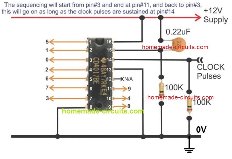
This sequencing and resetting is successfully carried out only as long as pin#15 is grounded or held at a logic low, otherwise the IC can malfunction. If it is held high, then the sequencing will not happen and the logic at pin#3 will stay locked.
Please note that the word “high” means a positive voltage that may be equal to the supply voltage of the IC, so when I say the outputs become high in a sequential manner means the outputs produce a positive voltage which shifts in a sequential manner from one output pin to the next, in a “running” DOT manner.
Pin 14 Needs External Frequency (Clock Signal)
Now the above explained sequencing or shifting of the output logic from one output pin to the next output is able to run only when a clock signal is applied to the clock input of the IC which is pin #14.
Remember, if no clock is applied to this input pin#14, it must be assigned either to a positive supply or a negative supply, but should never be kept hanging or unconnected, as per the standard rules for all CMOS inputs.
The clock input pin #14 only responds to positive clocks or a positive signal (rising edge), and with each consequent positive peak signal, the output of the IC shifts or becomes high in sequence, the sequencing of the outputs are in the order of pinouts #3, 2, 4, 7, 10, 1, 5, 6, 9, 11.
Pin 13 is Opposite of Pin 14
Pin #13 may be considered as the opposite of pin #14 and this pin out will respond to negative peak signals. Meaning if a negative clock is applied to this pin will also produce the shifting of "logic high" across the output pins
However normally this pin out is never used for applying the clock signals, instead pin #14 is taken as the standard clock input.
Therefore pin #13 needs to be assigned a ground potential, that means, must be connected to the ground for enabling the IC to function.
In case pin #13 is connected to positive, the whole IC will stall and the outputs will stop sequencing and stop responding to any clock signal applied at pin #14.
How Pin 15 Works Like reset Pin
Pin #15 of the IC is the reset pin input. The function of this pin is to revert the sequence back to the initial state in response to a positive potential or supply voltage.
Meaning, when a momentary positive voltage hits pin 15, the output logic sequencing comes back to pin #3 and begins the cycle afresh.
If the positive supply is held connected to this pin #15, again stalls the output from sequencing and the output clamps to pin #3 making this pinout high and fixed.
Therefore to make the IC function, pin #15 should always be connected to ground.
If this pinout is intended to be used as a reset input, then it may be clamped to ground with a series resistor of 100K or any other high value, so that an external positive supply now can be freely introduced to it, whenever the IC is required to be reset.
Using Pin#15 to Reduce the Number of Output Sequence
As I have explained above, there are 10 outputs in the pinout order of 3, 2, 4, 7, 10, 1, 5, 6, 9, 11.
The sequencing begins from pin#3 and ends at pin#11, where the IC resets and the sequence reverts to pin#3 to begin a new cycle.
However, suppose you do not want to use all the 10 output sequences, instead want to limit the sequence to 5 numbers only. Meaning, you want to use the output sequencing in order of 3, 2, 4, 7, 10. The sequence is supposed to begin from pin#3 and end at pin#10 and return back to pin#3.
However, this cannot happen as long as pin#15 is connected to ground. To limit the sequencing to a desired lower count, the pin#15 should be disconnected from the ground line, and connected to output pin which comes just after the last sequence pinout.
In the above example, where we want the sequence to end at pin#10, the next pinout that comes after pin#10 is pin#1, so pin#15 must be connected to this pin#1, to ensure that whenever the sequencing hits pin#1, it is instantly reverted to pin#3 for a new cycle, and the maximum output sequencing is limited to 5 count only.
In the above manner you can limit the output sequencing to any other desired count below 10.
Ground pin and Carryout Pin
Pin #8 is the ground pin and must be connected to the negative of the supply, while pin #16 is the positive and should be terminated to the positive of the voltage supply.
Pin #12 is the carry out, and is irrelevant unless many ICs are connected in series, I will elucidate it some other day. Pin #12 can be left open.
Have specific questions?? please feel free to ask them through your comments...all will be thoroughly addressed by me.
Basic IC 4017 Pinout Connection Diagram

Application LED Chaser Circuit using IC 4017 and IC555
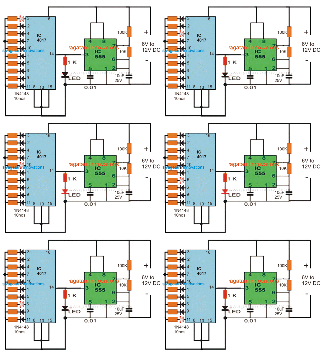
The following example GIF circuit shows how the pinouts of a IC 4017 is usually wired with an oscillator for obtaining the sequential logic high outputs. Here the outputs are connected to LEDs for indicating the sequential shift of the logics in response to each clock pulse generated by the IC 555 oscillator at pin#14 of the IC 4017.
You can see that the logic shift happens in response only to the positive clock or positive edge at pin#14 of the IC 4017. The sequence does not respond to the negative pulses or clocks.
IC 4017 Working Simulation

Video Clip:
How to Cascade Two 4017 ICs for Getting 17 Sequencing Outputs

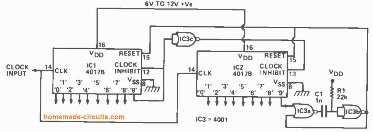
The diagram above shows how to connect two 4017s together to create a 10-to 17 stage counter/decoder. It shows how to cascade two 4017 ICs to get 17 sequencing outputs instead of only 10 from a single IC. The circuit is shown configured to divide by 17.
The clock signal is supplied in parallel to IC1 and IC2. As soon as the count falls below 9, the '9' output of IC1 turns low, causing the clock inhibit pin of IC2 to be set high through IC3c, preventing IC2 from being impacted by the clock signals.
The '9' output of IC1 rises high when the 9th clock pulse comes, inhibiting IC1 from further clocking action, while simultaneously driving the clock inhibit terminal of IC2 low through IC2c, allowing IC2 to respond to further clock signals.
When the 17th clock pulse arrives, the '9' output of IC2 swings high for a brief period, triggering the IC3a -IC3b 15uS monostable. This 15us pulse resets both counters to the empty or '0' states.
After that, the counting sequence starts again by itself. Because the '9' output of IC1 and the '0' and '9' outputs of IC2 are "lost" in the counting process, the circuit only has 17 counter/decoder stages available. By connecting the "free" input pin of IC2a to the matching output pin of IC2, the circuit can be made to count by any number between 10 and 17.
How to Cascade Three IC 4017 for Getting 25 Sequencing Outputs

The configuration for creating an 18 to 25 stage counter/decoder from three 4017s can be seen in the diagram above. IC3 is inhibited by IC4b and IC2's low output '9,' whereas IC2 is inhibited by IC4a and IC1's low output '9,' until the 9th clock pulse. Between the 10th and 17th clock pulses, IC1 is inhibited by its high '9' output, while IC3 is inhibited by IC4b and IC2's low output '9'.
Subsequently, between the 18th and 25th clock pulses, IC1 is inhibited by its high '9' output, and IC2 is inhibited through the high '9' outputs of IC1 and IC2 using IC4c, and the whole circuit is reset to the '0' state by means of the IC5a and IC5b monostable.
How to Cascade Four IC 4017 to get 33 Sequencing Outputs

Using a divide-by-33 operation, the above setup shows how to make a 26 to 33 stage counter/decoder set. By interposing extra IC2-1C5a-1C5b stages between 1C2 and 1C3, this design may be extended to provide a ny number of decoded output stages. Each subsequent 40178 stage adds eight decoded outputs to the system.


With over 50,000 comments answered so far, this is the only electronics website dedicated to solving all your circuit-related problems. If you’re stuck on a circuit, please leave your question in the comment box, and I will try to solve it ASAP!