The IC 555 is an extremely useful and versatile device which can be applied for configuring many useful circuits in the field of electronics. One very useful feature of this IC is its ability to generate PWM pulses which can be dimensioned or processed as per the needs of the application or the circuit.
What's PWM
PWM stands for pulse width modulation, a process which involves the control of the pulse widths, or the ON/OFF periods or logical outputs that's generated from a particular source such as an oscillator circuit or microcontroller.
Basically PWM is used for dimensioning or trimming the output voltage or power of a particular load as per individual or application requirements.
It is a digital way of controlling power and is more effective than analogue or linear methods.
There are many examples which illustrates the effective use of PWM in controlling the given parameters.
It's used for controlling the speed of DC motors, in inverters for controlling the RMS of the output AC or for producing modified sine wave outputs.
It can be also seen in SMPS power supplies for controlling the output voltage to precise levels.
It's also applied in LED driver circuits for enabling LED dimming functioning.
It's extensively used in buck/boost topologies for deriving stepped down or stepped-up voltages without using bulky transformers.
So basically it may be used for tailoring an output parameter as per our own preferences.
With so many interesting application options, does it mean the method may be too complicated or expensive to configure??
The answer is definitely, no. In fact it can be very simply implemented using a single IC the LM555.
There are basically two methods through which the IC 555 can be used for generating pulse width modulation output. The first method is using only a single IC 555, and a few associated parts such as a diodes, a potentiometer and a capacitor. The second method is by using a standard monostable IC 555 configuration and using an external modulation signal.
IC 555 PWM using Diodes
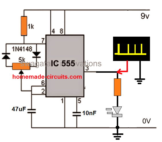
The first method is the simplest and effective, which uses the configuration as shown below:
Video Demonstration
The working of the above shown two diode IC 555 PWM circuit is quite simple. It's in fact a standard astable multivibrator design with the exception of an independent ON/OFF period control of the output.
As we know that the ON time of the IC 555 PWM circuit is decided by the time taken by its capacitor to charge at the 2/3rd Vcc level through pin#7 resistor, and the OFF time is determined by the discharging time of the capacitor below 1/3rd Vcc through the pin#7 itself.
In the above simple PWM circuit, these two parameters can be independently set or fixed through a potentiometer and through a couple of bifurcating diodes.
The left side diode which has its cathode connected with pin#7 separates the OFF time, while the right side diode which has its anode connected to pin#7 separates the ON time of the IC output.
When the potentiometer slider arm is more towards the left side diode, it causes the discharge time to decrease, due to lower resistance across the discharging path of the capacitor. This results in an increase in the ON time, and decrease in the OFF time of the IC PWM.
Conversely, when the pot slider is more towards the right side diode, it causes the ON time to decrease due to lowering of the resistance of the pot on the charging path of the capacitor. This results in an increase in the OFF period, and decrease in the ON periods of the IC output PWMs.
You can replace the timing resistors with a single potentiometer if you want to alter the duty cycle while keeping the frequency constant, as depicted in the following figure.
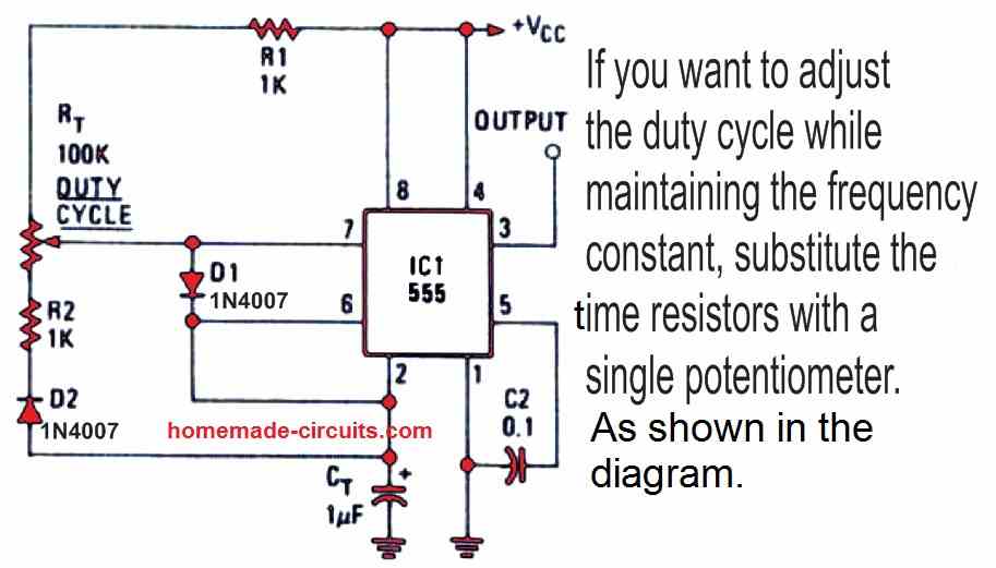
The 555 circuit may be adjusted as illustrated below to change the frequency while keeping the duty constant at around 50%.

2) IC 555 PWM using External Modulation
The second method is slightly complex than the above, and requires an external varying DC on pin#5 (control input) of the IC for implementing the proportionately varying pulse width at the IC output.
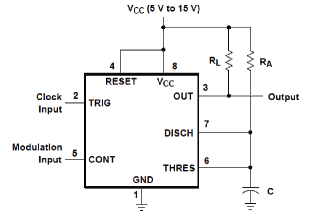
I have explained the following simple circuit configuration:
IC 555 Pinout
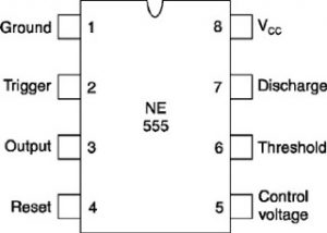
The diagram shows the IC 555 wired up in an easy monostable multivibrator mode. We know that in this mode the IC is able to generate a positive pulse at pin#3 in response to every single negative trigger at its pin#2.
The pulse at pin#3 sustains for some predetermined time period depending upon the values of Ra and C.We can also see the pin #2 and pin#5 assigned as clock and modulation inputs respectively.
The output is taken from the usual pin#3 of the chip.
In the above straightforward configuration the IC 555 is all set for generating the required PWM pulses, it just requires a square wave pulse or a clock input at its pin#2, which determines the output frequency, and a variable voltage input at pin#5 whose amplitude or the voltage level decides the pulse width dimensions at the output.
The pulses a pin#2 generates a correspondingly alternating triangle waves at pin#6/7 of the IC, whose width is determined by the RA and C timing components.
This triangle wave is compared with the instantaneous measure of voltage applied at pin#5 for dimensining the PWMs pulses at pin#3 output.
In simple words we just need to supply a train of pulses at pin #2 and a varying voltage at pin #5 for achieving the required PWM pulses at pin#3 of the IC.
The amplitude of the voltage at pin#5 will be directly responsible in making the output PWM pulses stronger or weaker, or simply thicker or thinner.
The modulation voltage can be a very low current signal, yet it would give the intended results.
For example suppose we apply a 50 Hz square wave at pin#2 and a constant 12V at pin#5, the result at the output will show PWMs with an RMS of 12V and frequency of 50Hz.
For reducing the RMS we just need to lower the voltage at pin#5. If we vary it the resultant will be a varying PWM with varying RMS values.
If this varying RMS is applied to a mosfet driver stage at the output, any load that is supported by the mosfet will also respond with correspondingly varying high and low results.
If a motor is connected to the mosfet, it will respond with varying speeds, a lamp with varying light intensities while an inverter with modified sine wave equivalents.
The Output Waveform
The above discussion can be witnessed and verified from the given waveform illustration below:
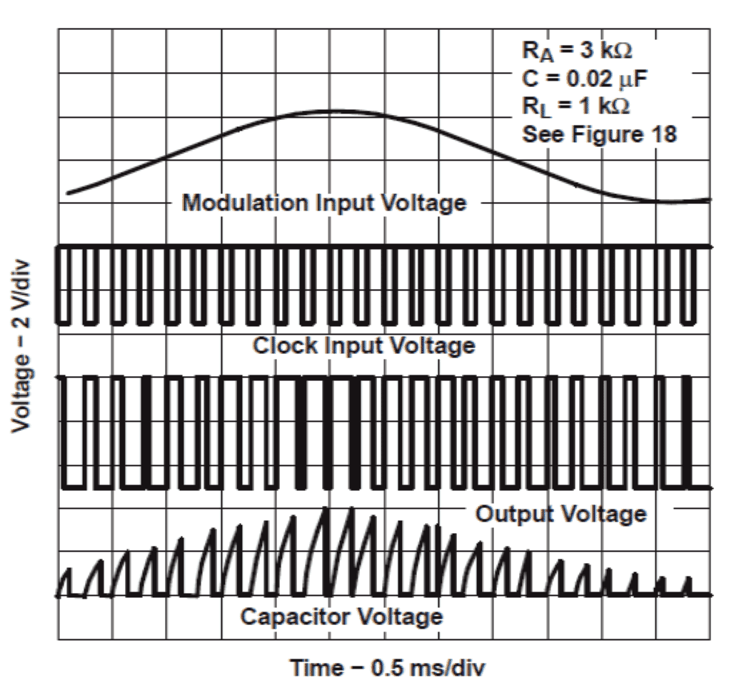
The topmost waveform represents the modulation voltage at pin#5, the bulge in the waveform represents the rising voltage and vice versa.
The second waveform represents the uniform clock pulse applied at pin#2. It's just for enabling the IC to switch at a certain frequency, without which the IC wouldn't be able to work as a PWM generator device.
The third waveform depicts the actual PWM generation at pin#3, we can see that the width of the pulses is directly proportional to the top modulation signal.
The pulse widths corresponding to the "bulge" can be seen as much wider and closely spaced which proportionately becomes thinner and sparse with the fall in the modulation voltage level.
The above concept can be very easily and effectively applied in power control applications as discussed earlier in the above article.
How to Generate a Fixed 50% Duty Cycle from a IC 555 Circuit
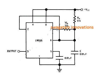
The following figure shows a simple configuration which will provide you with a fixed 50% duty cycle PWMs across its pin#3. The idea was presented in one of the IC 555 datasheets, and this design looks very interesting and useful for applications which need a simple and quick 50% fixed duty cycle generator stage.
