A varactor diode, also called varicap, VVC (voltage-variable capacitance, or tuning diode, is a type of semiconductor diode which features a variable voltage-dependent capacitance on its p-n junction when the device is reversed biased.
Reverse bias basically means when the diode is subjected to an opposite voltage, meaning a positive voltage at the cathode, and negative at the anode.

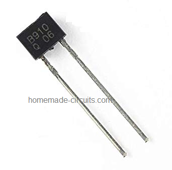
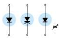
The way a varactor diode operates depends on the existing capacitance over the p-n junction of the diode while it's in a reversed biased mode.
In this condition we find a region of uncovered charges being established across the p-n sides of the junction, which together result in a depletion region across the junction.
This depletion region establishes the depletion width in the device, symbolized as Wd.
The transition in the capacitance due to the above explained isolated uncovered charges, across the p-n junction can be determined using the formula:
CT = ε. A/Wd
where ε is the permittivity of the semiconductor materials, A is the p-n junction area, and Wd is the depletion width.
How it Works
The basic working of a varicap or a varactor diode can be understood with the following explanation:
When a varactor or varicap diode is applied with a rising reverse bias potential, results in an increase in the depletion width of the device, which in turn causes its transition capacitance to decrease.
The following image shows the typical characteristics response of a varactor diode.
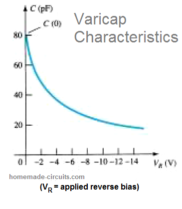
We can see the steep initial drop in CT in response to the increase reverse bias potential. Normally, the range for the applied reverse bias voltage VR for a variable voltage capacitance diode is restricted to 20 V.
With regard to the applied reverse bias voltage, the transition capacitance can be approximated using the formula:
CT = K / (VT + VR)n
In this formula, K is a constant as determined by the type of semiconductor material used and its constructional layout.
VT is the knee potential, as described below:

VR is the amount of reverse bias potential applied on the device.
n can have the value 1/2 for varicap diodes using alloy junction, and 1/3 for diodes using diffused junctions.
In the absence of a biasing voltage or at a zero voltage biasing, the capacitance C(0) as the function of VR can be expressed through the following formula.
CT(VR) = C(0) / (1 + |VR/VT|)n
Varicap Equivalent Circuit
The standard symbols (b) and an equivalent approximate circuit (a) of a varicap diode is represented in the following image:

The right side figure provides an approximate simulation circuit for a varicap diode.
Being a diode and in the reverse biased region, the resistance in the equivalent circuit RR is shown significantly large (around 1M Ohms), while the geometric resistance value Rs is quite small. The value of CT may vary between 2 and 100 pF depending on the type of varicap used.
In order to make sure that the value RR is sufficiently large, so that the leakage current can be minimum, a silicon material is normally selected for a varicap diode.
Since a varicap diode is supposed to be specifically used in extremely high frequency applications, the inductance LS cannot be ignored even though it may look small, in nanohenries.
The effect of this small looking inductance can be a quite significant, and can be proved through the following reactance calculation.
XL = 2πfL, Let's imagine, the frequency to be at 10 GHz, and LS = 1 nH, will generate in an XLS = 2πfL = (6.28)(1010 Hz)( 10-9 F) = 62.8 Ohms. This looks too big, and no doubt this is why varicap diodes are specified with a strict frequency limit.
If we suppose the frequency range to be appropriate, and the values of RS, XLS to be low compared to the other series elements, the above indicated equivalent circuit could be simply replaced with a variable capacitor.
Understanding Datasheet of a Varicap or Varactor Diode
Complete Datasheet of a typical varicap diode can be studied from the following figure:
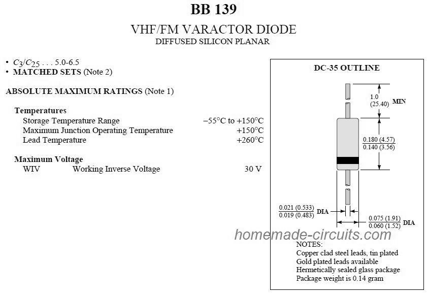
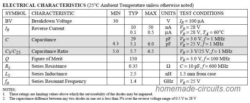
The ratio of C3/C25 in the above figure, demonstrates the ratio of the capacitance level when the diode is applied with a reverse bias potential between 3 to 25 V. The ratio helps us to get a quick reference regarding the level of change in the capacitance with respect to the applied reverse bias potential.
The figure of Merit Q provides the range of consideration for implementing the device for an application, and it is also a rate of the ratio of energy stored by the capacitive device per cycle to the energy lost or dissipated per cycle.
Since the loss of energy is mostly considered as a negative attribute, higher the relative value of the ratio, the better.
Another aspect in the datasheet is the resonant frequency of a varicap diode. And this is determined by the formula:
fo = 1/2π√LC
This factor decides the application range of the varicap diode.
Capacitance Temperature Coefficient
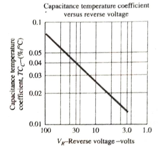
Referring to the above graph, the capacitance temperature coefficient of a varicap diode may be evaluated using the following formula:

where ΔC signifies the variations in the capacitance of the device due to change in temperature represented by (T1 - T0), for a specific reverse bias potential.
In the above datasheet for example, it shows C0 = 29 pF with VR = 3 V and T0 = 25 degrees Celsius.
Using the above data we can evaluate the change in the capacitance of the varicap diode, simply by substituting the new temperatures T1 value and the TCC from the graph (0.013). Having the new VR, the TCC value can be expected to vary accordingly. Referring back to the datasheet, we find that the maximum frequency attained will be 600 MHz.
Using this frequency value, the reactance XL of the varicap can be calculated as:
XL = 2πfL = (6.28)(600 x 1010 Hz)(2.5 x 10⁻⁹ F) = 9.42 Ohms
The result is a magnitude which is relatively small and it's acceptable to ignore it.
Application of Varicap Diode
Few of the high frequency application areas of a varactor or varicap diode determined by low capacitance specs are adjustable bandpass filters, automatic-frequency-control devices, parametric amplifiers, and FM modulators.
The example below shows varicap diode implemented in a tuning circuit.
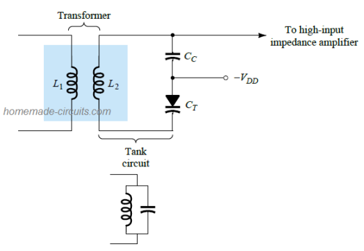
The circuit consists of a combination of L-C tank circuits, whose resonant frequency is determined by:
fp = 1/2π√LC'T (a high-Q system) having a C'T level = CT + Cc, established by the applied reverse-bias potential VDD.
The coupling capacitor CC ensures the required protection against the shorting tendency of L2 the applied biasing voltage.
The intended frequencies of the tuned circuit are subsequently allowed to move to the high-input impedance amplifier for the further amplification.
Need Help? Please Leave a Comment! We value your input—Kindly keep it relevant to the above topic!