The IC 555 astable multivibrator is a configuration where the IC 555 output continuously switches between an ON state and an OFF state at a given frequency, determined by its RC timing components. Since in this configuration, the output of the IC 555 is never in a stable state, it is called an astable multivibrator.
A typical 555 astable multivibrator circuit can be seen in the following figure.
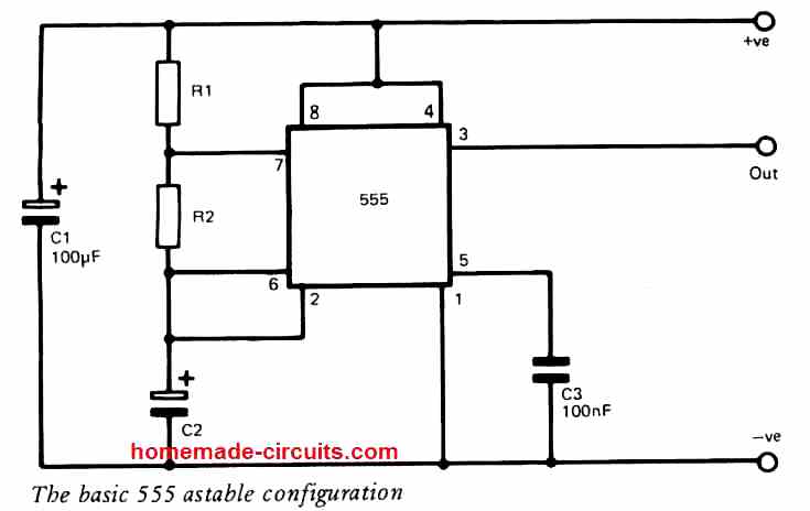
The design is actually a kind of relaxation oscillator where C2 is first allowed to charge to 2/3rd of the supply voltage via resistors R1 and R2, and then it is discharged by means of R2 to 1/3rd of the supply voltage. The working frequency is thus determined through the values selected for resistors R1, R2 and the capacitor C2, which may be calculated using the formula:
Frequency = 1.44/(R1 + 2R2)C2
The reason for incorporating the R1 value twice the value of R2 (instead of simply using both values identical) is that R2 is used during both the charge and discharge paths of C2 and so it has two times more effect than R1. Common magnitudes for the timing parts will be 4k7 for R1 and R2, and 100nF for C2, which would provide an operating frequency of approximately 1kHz (4k7 + 2(4k7) = 14k1 x 100 nF = 0.00141, and 1.44 divided by 0.00141 = 1021Hz or 1.021kHz.
The operating frequency could be altered by modifying the value of the C2 capacitor. Altering the value of C2 would produce an inversely proportional variation in frequency (for example if you double the C2 value will cause the frequency output to be halved and vice versa).
Likewise, the operating frequency could be modified by changing the value of the timing resistance which would again result in an inversely proportional results for the frequency of the astable circuit.
Component Value Limitations
There is definitely some limitations for the part values, and therefore it is recommended to ensure that the combined values of R1 and R2 always stays below 10 Megohms.
A resistance which may be significantly bigger than 10 Meg might rather produce unstable effects or may possibly cause the circuit oscillations to completely collapse. The main reason for this is the extremely reduced currents into the timing circuit, resulting in too low input currents for the 555 astable functioning or may be due to leakage in capacitor C2.
Additionally there is a limitation on how small R1 resistor can be, and this may be determined by dividing the supply voltage by 0.2. This could, for instance, offer a value of 45 ohms using a 9 volt supply.
Practically speaking, it is usually essential to work with a value that is much larger than this absolute lowest magnitude. The main reason for this is basically to maintain the IC 555's dissipation to a reduced and acceptable level.
It must additionally be kept in mind that an internal transistor of the IC 555 generates a virtual short circuit between IC 555's pin 7 and the negative supply line during the time the capacitor C2 goes through a discharging process. And, besides affecting the IC 555 alone, a lower R1 value could result in a high dissipation through this resistor itself, leading to an extremely high current draw each time the capacitor C2 discharges.
A lowest possible value of around 1 K thus looks to be far more reasonable. Pin 3 which is the output of the IC 555, turns high during the time C2 charges and pin#3 switches to a low while C2 begins discharging. This charge/dischage pattern produces a rectangular waveform at the pin#3 output of the IC 555.
This means that the output of the IC 555 atable multivibrator is generally not a squarewave it is not feasible to get a square wave output having one-to-one mark-space ratio, from this fundamental construction. This is mainly because C2 is allwed to charge via the resistor R1 and R2 combined, however it is able to discharge solely via the resistor R2.
For this reason charge (high) time should be higher than the discharge (low) time. In certain implementations this could be preferable, and in others it might be unimportant, however as we will find later on it is easy to implement any preferred mark-space ratio with the help of a personalized astable setup.
The IC 555 output allows a peak to peak voltage which is nearly equal to the circuit's supply voltage level, and this output is a low impedance in nature.
Output Current Specs
The IC output resembles a class B amplifier stage, and therefore is able to source or sink up to 200 mA. It is also possible to extract an output signal across the terminals of capacitor C2, but this will provide a very low output current and is generally not advisable because any loading across C2 may have a serious impact on the charging and discharging rhythm of C2.
As the values of R1 and R2 increases, this causes the output current to also reduce proportionately. If you check the waveform across C2 you will find it to be approximately triangular in shape, although the charging and discharging pattern of C2 being exponential in nature therefore the triangular waveform is not linear.
Furthermore, much like the pin#3 output characteristics, the mark-space ratio or the PWM signal is not perfectly symmetrical. Even with these types of drawbacks, the signal across C2 can generally be useful in many applications like modulated pulse generators and musical effects generators.
A minor disadvantage of' the IC 555 is that if the output supply is shunted causes a negative voltage spike to be injected onto the supply rails of th circuit. In order to decouple these spikes we can use the capacitor C1 as indicated in the diagram.
However, even with the presence of C1 in the circuit it may often be not possible to counter these negative spikes. Capacitor C3 also works like a decoupling capacitor, and this eliminates all stray signal pick-up on pin#5 of the device.
How to Use Control Voltage Pin#5
An advantage of the control voltage pin#5 is that, the astable oscillator output at pin#3 of the Ic can be modulated through a suitable frequency or voltage level applied at pin#5. However, if no external modulation is applied at pin#5, then this pinout must be decoupled through a grounding 10 nF capacitor, so that the IC output does not get unnecessarily modulated through stray frequency pick-ups at pin#5.
All electronic circuit is only going to work within the range of specific supply voltage limits, and this is one thing that should generally be remembered. For the IC 555 the lowest and highest supply voltage values are between 5 V and 1 5 V.
It is generally not recommended to operate the IC 555 above 15 V, which can otherwise cause severe or permanent damage to the device. The highest working frequency of the IC is around 500 kHz, however, the low frequency limitation is normally not specified for the IC 555.
Timing Capacitor Value
The minimum output frequency limit of the IC is dependent on how good the timing capacitor C2 is, and to ensure proper working with extremely low frequencies, timing capacitor C2 must be preferably a polarized type like tantalum or electrolytic.
Although theoretically it can be completely okay to work with a timing capacitor as large as 100 uF with a total timing resistance of many megohms, practically such high combinations may completely fail to work.
In such situation, the capacitor's leakage resistance could be around a few hundred kilohms, and this might restrict the charge voltage to a magnitude which would inhibit the proper functioning of the astable circuit.
Using Astable with Low Frequencies
When IC 555 astable multivibrator circuit is intended to work with lower frequencies, it is usually desirable to assess the frequency with regards to output high times and low times instead of frequency. The high time may be calculated using the formula
Th = 0.685 (R1 + R2)C2
The low time is given by the formula:-
T1 = 0.685R2C2
There isn't any lowest limit for the C2 value actually, and even in the absence of an external capacitor C2, the IC 555 astable circuit might most definitely oscillate with a frequency dependent on the internal capacitance of the device which is around 30pF. To be able to get trustworthy and constant output frequency, it is best to incorporate a timing capacitor which must be at least about 1nF in magnitude.
A feature which at times may be useful, particularly when the 555 is implemented with extremely low frequency configurations, is that the first half of the first output cycle might have a longer time interval than the cycles which subsequently follows afterwards.
This is basically because of C2 beginning with zero charge for the initial cycle, while for the subsequent cycles it starts with a charge that is equivalent to 1/3rd of the supply voltage. This specification is actually not exclusive to the IC 555 astable: to be precise this feature is seen in most of the simple C/R based astable oscillators which generate slightly longer periods for the initial or the starting pulse cycle.
Gated Astable
The 555 could be applied like a gated astable oscillator, as indicated in the following figure. Meaning, the IC 555 astable can be enabled or disabled from an external source.
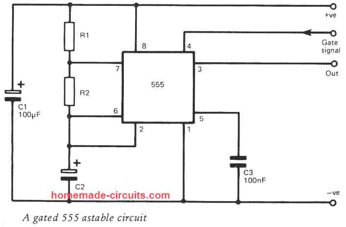
This configuration is essentially identical to the circuit demonstrated in the previous astable design, except the pin#4 of the IC 555 which here can be seen connected with the input gating signal, instead of the positive line. It is required to pull the Pin#4 under around 0.5 volts to be able to shut off the 555 internal oscillator, which can force the output of the IC to go low as soon as the circuit is gated off.
If the pin#4 is left open or unconnected, the astable may keep oscillating anyway.
Adjustable Duty Cycle
As discussed previously, it is easy to create a 555 astable multivibrator circuit designed to generate any desired mark-space ratio duty cycle. The design for this type of astable circuit can be witnessed in the following figure.
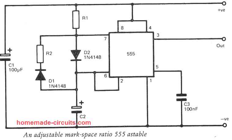
The circuit includes guiding diodes D1 and D2 which channelize the charging current for the timing capacitor through R1 and the discharge current through R2. This arrangement thus helps to generate a 1 : 1 mark-space ratio simply by selecting the R1 and R2 values perfectly identical.
lf the value of R1 is selected bigger than R2, causes the full charge time (output high) to be proportionately lengthier than the full discharge time (output low). On the other hand, allowing R2 to be bigger in value than R1 causes the discharge time to be proportionately lengthier than the charge time.
The equations for determining the operating frequency and high output time are somewhat different because R2 is eliminated from the path while C2 is charging. Hence while calculating the frequency the timing resistance is basically R1 + R2 and not R1 + 2R2 as in the standard astable formula for IC 555.
Likewise, while calculating the high output time, the timing resistance is only R2 and not R1 + R2. The involvement of the two diodes have practically no effect on the frequency, charge, and discharge times.
Frequency Modulation
As pointed out before, the IC 555 astable's operating frequency could be modulated through an external control voltage, which is exhibited in the following figure.
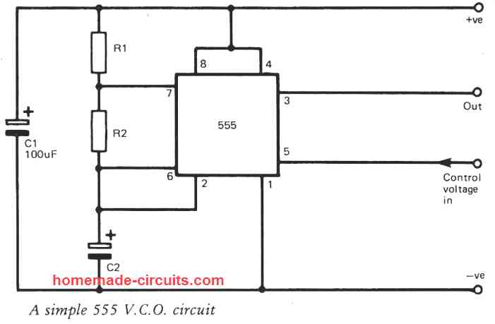
This configuration is similar to the standard 555 astable setup except the pin#5 decoupling capacitor which can be seen missing and the control voltage injected to this pin#5. This control voltage pinout of the IC is internally linked with a resistive divider network that fixes the 2/3rd supply voltage threshold limit, enabling the IC 555 to flip from the charge mode to the discharge mode.
When pin#5 potential is pulled over 2/3rd of the supply voltage, causes the frequency of the IC 555 to reduce because C2 now has to charge to, and discharge from, a higher voltage level, which delays the ON/OFF process and makes it longer.
When pin#5 is applied with a potential below 2/3rd of the supply voltage, it causes a decrease in the charging/discharging voltage across C2. This allows both the frequency ON/OFF processes to consume less time, causing the operating frequency to increase. However, there is no change in the output waveform at pin#3, but there may be a little change in the shape of the waveform and the amplitude of the signal across C2.
If we see the internal layout of the IC 555 we find that pin#5 is attached directly to the internal potential divider. Due to this the threshold voltage where the IC switches from the charge state to the discharge state is not identical to the voltage introduced at pin#5. This condition restricts the amount of control which you can get through an external control voltage at pin#5 of the IC.
Due to this the output frequency drops by slightly more than 50% when the control voltage at pin#5 is made as high as the positive supply voltage. The output frequency can be increased a bit higher than twice if the control pin#5 is held at 1/3rd of the supply voltage, and this could be enhanced even slightly more when pin#5 voltage is held a little bit lower.
On the other hand, if we pull the pin#5 potential extremely low, the IC could malfunction and you may find the output frequency reducing to a great level. Hence, it is recommended to maintain the control voltage at pin#5 between 1/3rd of the supply voltage and the full supply voltage range.
Tone Generator
The IC 555 is a valuable device for applications which requires an audio tone to be reproduced over a speaker with reasonably loud volume. Driving a loudspeaker directly through the output of the IC 555 is definitely possible due the ICs 200 mA output current capacity. However, the direct connection of the loudspeaker at pin#3 could turn a bit inefficient causing the IC to malfunction.
It is therefore recommended to add a high value capacitor in series with the pin#3 and the loudspeaker. Although we can see a high impedance loudspeaker indicated in the Figure below, the circuit can actually function using a low impedance 8 ohm type speaker also, but in most cases a high impedance loudspeaker would deliver satisfactory volume.
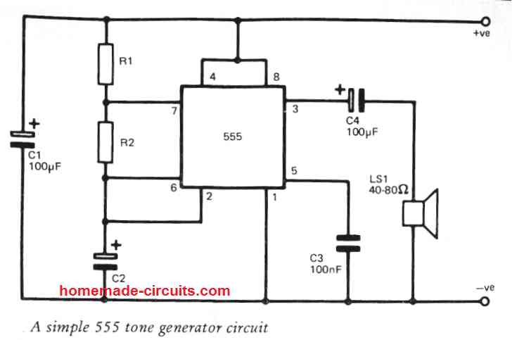
You can expect an output power of a few hundred milliwatts from the IC 555 astable output into any 8 ohm load or a loudspeaker. However, you must be careful in such applications considering that several smaller loudspeakers are only able to handle a power input of 200 mW approximately.
Other than the normal implementations of the IC 555 astable as discussed in the previous paragraphs, it is easily possible to combine the various astable configurations explained thus far to offer (for example) a gated, frequency modulated tone generator, or a gated squarewave generator to create innovative IC 555 circuits. Due to the great versatility and its affordable cost the IC 555 has been so far successful in becoming one of the most popular ICs among the hobbyists.