In this post I have explained how to make simple yet fully stabilized and regulated, variable power supply circuits using the IC 741 op amp.
Three versions of the 741 power supplies are I have explained below:
- Simple Low Current Adjustable Power Supply
- Stabilized, High Current Variable Power Supply
- Stabilized, High Current Variable Power Supply, with Short Circuit protection.
Simple Variable IC 741 Power Supply
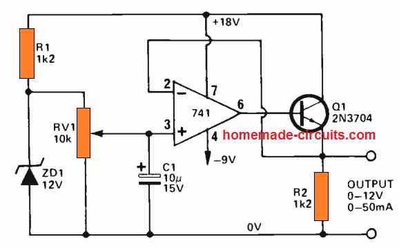
The first figure below exhibits a IC 741 based simple variable voltage power supply. This design provides a stabilized output that can be thoroughly adjusted, from 0V to 12V with current ranging up to a maximum of 50 mA.

The circuit working is very basic.
The zener diode ZD is gets the supply from the positive line through resistor R1. A fixed reference voltage of 12V is produced over the zener diode, which is supplied to an adjustable voltage divider RV1.
The divider output is completely adjustable from 0V to 12V, which is applied to the non-inverting input of the op amp 741.
The op amp is configured like an unity gain voltage follower, with transistor Q1 rigged in the form of an emitter follower current amplifier stage, connected in series with its output.
Therefore, the output voltage from the power supply circuit tracks and follows the voltage established at the input of the op amp input by means of RV1, which is totally adjustable from 0V to 12V.
Remember that this specific 741 power supply circuit employs an 18V positive supply and a 9V negative supply.
Additionally, the output voltage range of the present circuit could be made higher through the use of higher rated zener diode and through the supply of higher rated unregulated input supply voltages.
The specifications of the current could be likewise made higher by incorporating a couple of more power transistors in place of the existing transistor Q1.
3 V to 30 V IC 741 Power Supply
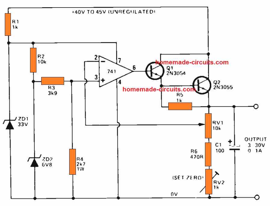
The next figure indicates the way a 741 op amp could be employed as the basic foundation of a regulated power supply unit, that comfortably handles the output range from 3V to 30V, with currents ranging up to 1A.

In this configuration, the supply to the 741 op amp is stabilized at 33V by using the zener diode ZD1.
Another extremely temperature stabilized, constant reference voltage of 3V is achieved through the zener diode ZD2, and this applied to the non inverting input of the IC 741 .
The transistors Q1, Q2 are connected with the output of the op amp, and are configured like a variable gain non inverting d.c. amplifier.
This set up has a gain which can be varied from unity to x10, by means of RV1.
This provides an output voltage that is completely adjustable from 3V to 30V through the pot RV1.
The output voltage generated by this IC 741 power supply features a fully stabilized voltage using a negative feedback loop.
Over-Current and Short Circuit Protected 741 Power Supply
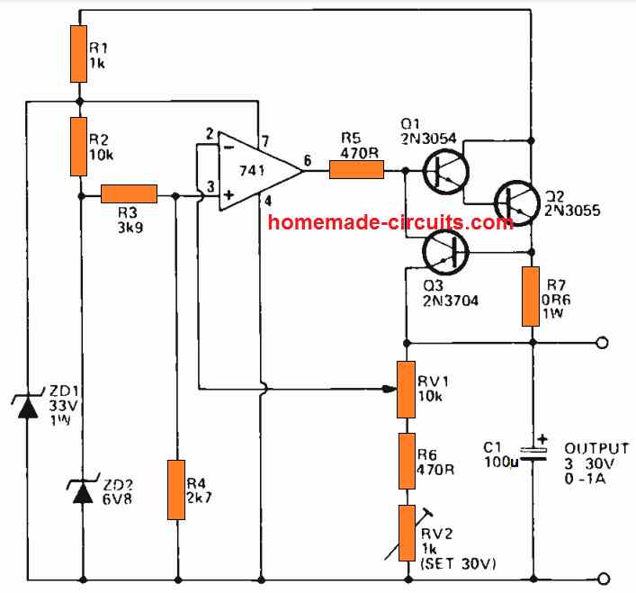
The last figure below explains the manner in which an overload protection could be added to the previous IC 741 power supply circuits.
In this design we use a current sensing resistor R7, connected in series with the regulator output.

The transistor Q3 which is the shut-down transistor is powered through this resistor R7 and is configured such that its base-collector junction has the ability to short the Q1, Q2 base-emitter junction of the output transistor stage.
Typically, Q3 stays deactivated, and it does not effect the functioning of the circuit.
However, as soon as the output currents of the power supply reaches beyond the 1A mark, a voltage difference of over 600 mV is produced across R7, it instantly begins biasing the transistor Q3 base, switching it ON.
As a result Q3 is forced to shunt the base-emitter junction of the Q1-Q2 output stage to ground.
Consequently, the action causes an instant reduction of the output current, generating a large negative feedback across the connected loop. This action causes an automatic limiting of the output current within the 1A range.
The same procedure is implemented during a short-circuit conditions also, providing a full short circuit and over load protection to this IC 741 power supply circuit.
Improved Design
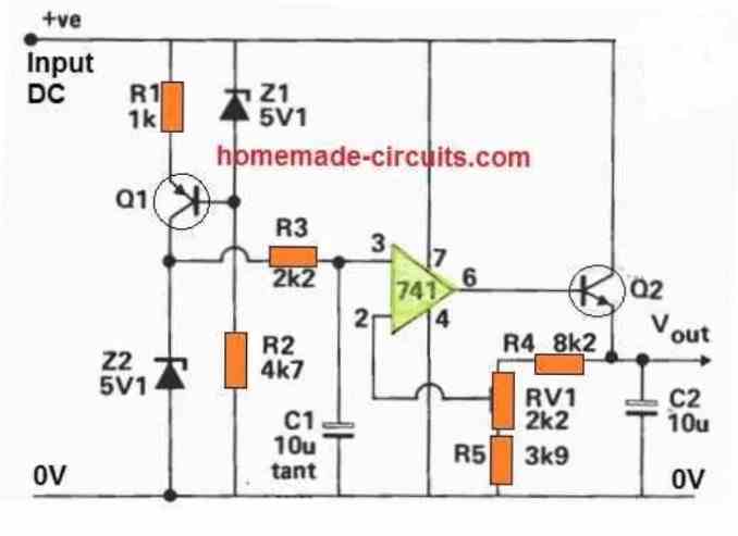
This power supply differs from the previous one in a number of ways. The R12, Q1 Z1 network runs the reference zener Z2 at nearly constant current.
As a result, Z2 is substantially less susceptible to supply changes such as ripple and uncontrolled supply. The R3 C1 (7 HZ low pass) filter significantly decreases the zener diode's ripple voltage and interference.
The output voltage may be changed using the preset VR1.

A precise voltage reference must be implemented if an extremely accurate power supply is desired.
Temperature coefficients as low as 10 ppm / degrees C can be used to get these results.
High stability resistors (TC = 10 ppm / degrees C) and a low drift op amp must be employed while applying this degree of stability.
A main supply filter must also be used to prevent mains transmitted noise (mostly loud clicks caused by electric motors and thyristors going on).
This is a low pass filter network using a passive inductor capacitor that reduces high frequency transients and pops.