

In this article I have explained a couple of inverter circuits featuring an automatic feedback control for ensuring that the output does not exceed the normal specified AC output level, and also does not exceed the specified overload conditions.
What is Feedback Control in Inverters
A feedback control in inverter is generally incorporated to control the output voltage and output current and prevent it from exceeding beyond dangerous limits.
In this system, the output AC mains voltage is first dropped to a proportionately lower level, and fed to the shut down pin of the control IC. The stepped down feedback voltage now follows the output AC and varies up/down accordingly, in a proportionate manner.
The control ICs shut down circuitry comares and monitors this feedback signal with a fixed ference derived from the battery volatge of the inverter.
In an event that the output voltage tends to rise above the predetermined value, and increase beyond the reference level, it activates the error amplifier, which shuts down the inverter output PWM. Once this happens, the output voltage instantly dips, causing the feedback signal to decrease below the reference value. This situation prompts the shut down feature of the IC to get disabled, and the IC starts working normally again.
If the output yet again tries to rise beyond the unsafe level, the above process is repeated in the identical manner, and this goes on continuously and rapidly, ensuring that the output voltage is never allowed to surpass the specified unsafe level.
Feedback Control in SG2524/SG3524/SG3525 Inverters
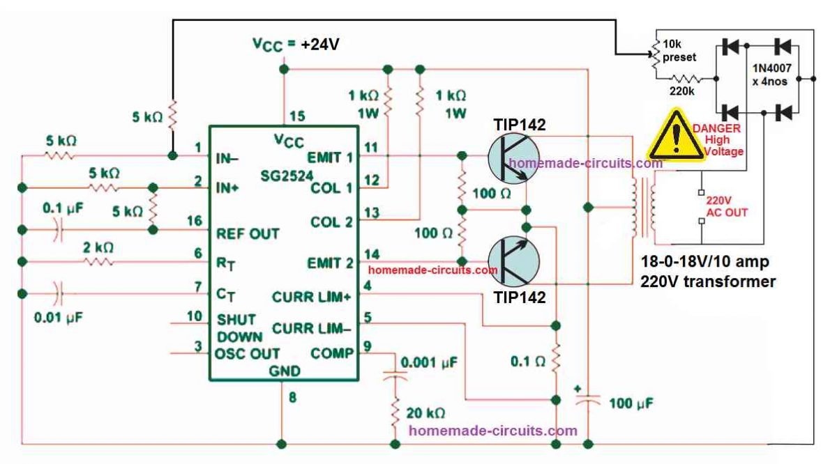
The first example circuit belw shows how an automatic feedback control can be added to a SG2524 inverter circuit. The same concept can be also applied to all the other inverter versions, using the IC SG3524, and SG3525.

You can refer to the following two datasheets for exactly knowing how the pinouts of the IC SG2524 IC are designed to function:
The feedback control loop is configured in the following can be understood with the following points:
The 220V AC output is first rectified using a 4 diode bridge rectifier circuit.
The rectified high voltage DC is dropped to a lower DC level, at around 5V to 10V through the voltage divider network built using the 220K resistors and the 10K preset.
The 10K preset is used to adjust the feedback voltage until the output voltage is controlled just at the right level.
The feedback is taken from the 10K preset's center arm and fed to the error amplifier's non-inverting input pin#1 of the IC 2524.
This error amplifier is nothing but an opamp set internal to the IC for controlling the PWM of the output pin#11 and Pin#14.
The inverting or the (+) input pin#2 of the op amp is clamped at a fixed reference level of +2.5V through the couple of voltage divider resistors configured around the pin#2 and pin#16 of the IC. The +5V reference potential is derived from pin#16 of the IC and then dropped to 2.5V using the two voltage divider resisters.
Since the pin#2 of the error amplifier is fixed at 2.5V reference, means that if the pin#1 of the opamp rises above the 2.5V level would instantly trigger the PWM feature of the IC, causing narrowing of the output PWM to the transistors.
The feedback 10k preset is adjusted in a such a way that feedback voltage at pin#1 reaches the 2.6 V mark as soon as the output voltage reaches the specified unsafe high voltage level.
In such situations, when the pin#1 receives a 2.6 V, it will cause the internal error amp to activate, narrowing the output PWMs to the transistors, which will in turn cause the output voltage to reduce to the safe lower levels, appropriately.
Adding Feedback in IC 555 Inverter
You might have already gone through the post which explains how to build simple 555 based inverters.
Although all these inverters are decently designed and will produce the intended 220 V or 120 V from an easy IC 555 set up, these do not have a built-in feedback system for ensuring a constant output voltage.
The following figure shows how an ordinary IC 555 inverter could be transformed into an enhanced inverter through an easy feedback loop control network.

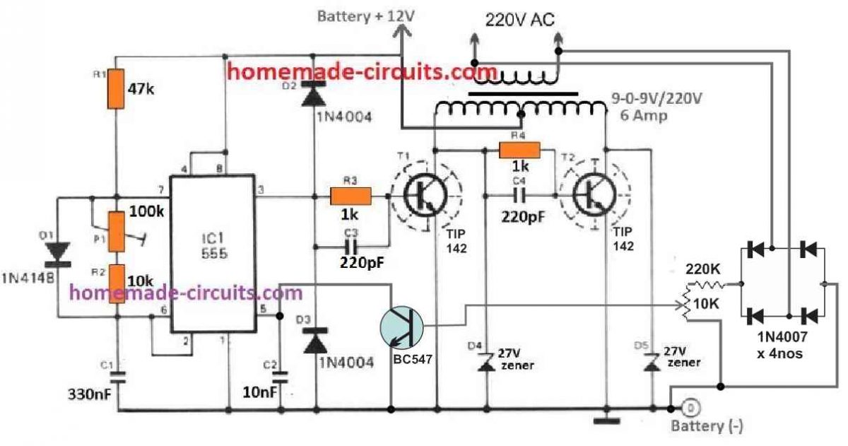
In this circuit also, we find that the 220V output from the transformer is first rectified to a DC level, and then it is stepped down through a resistive network comprising of a 220K resistor and a 10k preset.
The 10k preset center lead is configured with the NPN transistor BC547, whose collector can be seen connected with the pin#5 of the IC which is control input of the IC.
We know that normally when pin#5 is open, the PWM at the output pin#3 of the IC has a maximum PWM, however, as the potential at pin#5 is reduced, the output PWM also gets reduced proportionately.
Grounding the pin#5 causes the output PWM at pin#3 to become very narrow, with almost zero average voltage at this pinout.
In the IC 555 feedback circuit, when the output voltage tends to rise above the unsafe high voltage threshold, as per the setting of the 10k preset, the base of the BC547 slowly starts getting biased. When this happens, the BC547 begins conducting and causes the pin#5 of the IC to get gradually grounded. The grounding of the pin#5 of the IC causes the output PWM at pin#3 to get narrower, which in turns causes the output voltage to drop to the normal levels.