Although a variety of laboratory power supplies have appeared in recent times, only handful of these will provide you with the efficiency, versatility, and low cost of the design detailed in this article.
In this article I have explained a highly regulated, DIY, laboratory grade power supply with dual 0-50 volt. The voltage and current ranges are independently variable from 0 to 50 V, and 0 to 5 amps respectively..
Having said that, because of the DIY layout, you can customize the settings as needed, which can witnessed in the following specification table..
- Number of Supplies = 2 (Fully Floating)
- Voltage Range = 0 to 50V
- Current Range = 0 to 5 amps
- Coarse control and Fine Control ratio for both current and voltage = 1:10
- Voltage Regulation = 0.01% line, and 0.1% load
- Current Limiter = 0.5%
You Will Also Like: How to Design a Bench Power Supply Circuit
Circuit description

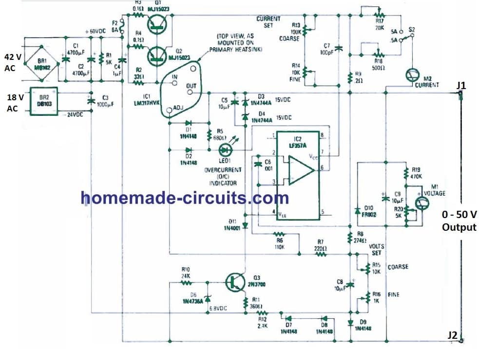
Figure 1 above shows the circuit diagram of the laboratory power supply. The specifications of the layout is centered around IC1, an LM317HVK adjustable regulator, for wide-ranging functionality. The "HVK" suffix suggests the high-voltage edition of the regulator.
The remaining portion of the circuit enables voltage setting and current limiting capabilities. The input to IC1 originates from the output of BR1, which is filtered by C1 and C2 to around + 60 volts DC, and the input for current-sense comparator IC2 develops from bridge rectifier BR2, which furthermore works like a negative bias supply to get regulation to ground level.
The function of IC1 is to keep the OUT terminal at 1.25 volts DC over the ADJ terminal. The current drain at the ADJ pin is extremely minimal (as low as 25 µA) and, therefore, R15 and R16 (the crude and refined voltage manipulations) and R8 form a voltage divider, with 1.25 volts showing up around R8.
The lower terminal of R16 attaches to a -1.3 reference volt developed by D7 and D8, permitting the R8 - R15 resistive divider fix the output voltage right down to ground level any time R15 + R16 becomes 0 ohms.
Calculating the Output Voltage
Generally speaking, the output voltage depends upon, the following results:
(VouT - 1.25 + 1.3) / (R15 + R16) = 1.25 / R8.
Thus, the highest magnitude of voltage value available from each variable supply board can be:
VOUT= (1.25 / R8) x (R15 + R16) = 50.18 volts DC.
Potentiometers R15 and R16 is used for controlling the output voltage, which enables the VouT to vary from 0-50 volts DC.
How Current Control Works
When the DC load current increases, the voltage drop across R2 also rises, and at around 0.65 volts (that is relative to around 20 mA), Q1 and Q2 switch on, becoming the primary course of the current. Additionally, R3 and R4 guarantee that Q1 and Q2 handle the load uniformly. IC2 works like a Current limiter stage.
Its non-inverting input makes use of the output voltage like a reference, while its inverting input is attached to the voltage divider developed by R6 and the current control pots R13 and R14. The voltage drop across R6 is about 1.25 volts, the reference voltage stated above is determined by the difference across the IC1 terminals OUT and ADJ.
Current passing across Q1 and Q2 moves via R9, building a voltage drop across R13 + R14. As a result, IC2 is forced to switched OFF as soon as the voltage drop around R9 generates current by means of R13 and R14, causing the non-inverting input voltage to go beyond VouT.
This fixes the current limiting threshold at: (IouT x 0.2)/(R13 + R14) = 1.25/100K; low = 0 to 5 amps. This provides a corresponding a range of around 0-5 amps.
When the current limit threshold is reached, output of IC2 becomes low, driving the ADJ pin down by way of D2 and resulting in the illumination of LED1. Extra current for D5 is delivered by R5.
As the ADJ pin is driven low, the output follows, until the output current falls to a point equivalent to the setting of R13 and R14.
Considering that the output voltage could be between 0-50 volts, the supply voltage for IC2 should follow this range working with D3, D4, and Q3.
Then, D9 ascertains that the output voltage won't increase once the supply input is turned off, while D10 safeguards against a reverse supply voltage. Lastly, the meters M1 displays the voltage reading and M2 displays the current reading.
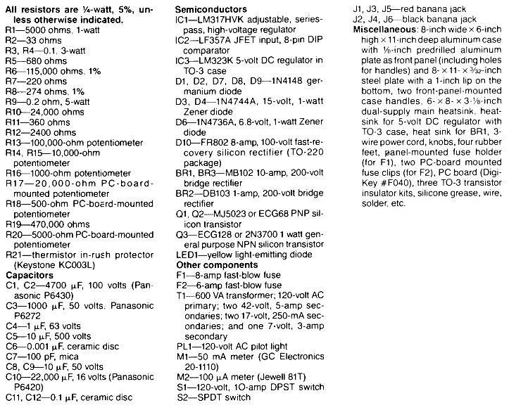
Parts List
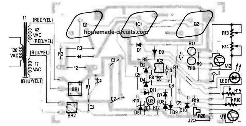
PCB Layout Design
Another Simple Laboratory Power Supply Circuit using LM324 IC
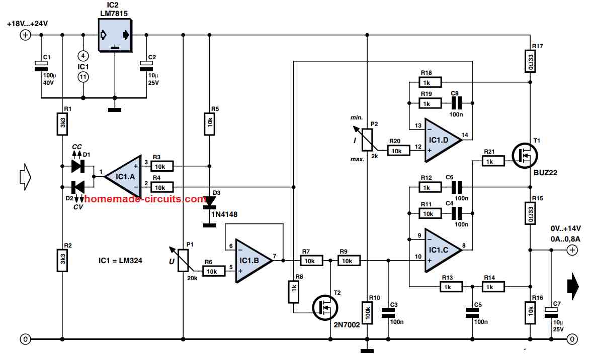
To obtain an intermediate supply voltage the regulator IC LM7815 has been used here. Its output travels by means of R17, that reads the output current, for th MOSFET T1.
This MOSFET is operated through the opamp IC1, configured like a voltage regulator. In this laboratory power supply circuit R11 and C4 establish the control loop's bandwidth, which enables the elimination of oscillation at increased frequencies.
Resistor R15 guarantees that capacitive loads having reduced effective resistance will not cause the control loop to become unstable. The AC content's negative feedback of the current through R12 and C5 enables the circuit to be perfectly reliable even while a large capacitor is employed at its output of the power supply.
The DC content's negative feedback through the low-pass filter is established by resistor R14 and capacitor C6. This configuration guarantees that the voltage drop developed across the resistor R15 is effectively compensated for.
The output capacitor C7 delivers a low impedance source for high-frequency loads. The resistor R16 helps the discharge of the capacitor C17 whenever the set voltage is decreased in the absence of an output load.
The IC1D section works like a current regulator. Once again in order to make sure the lab power supply works with perfect stability, the feedback loop's bandwidth is restrained by the resistor R19 and the capacitor C8.
In case the voltage drop developed across the resistor R17 becomes higher than the value as adjusted by the preset P2, the current limiting feature of the circuit kicks in and the transistor T2 is triggered ON.
This action subsequently cuts down the input voltage to the voltage regulation circuit stage until the specified amount of output current is arrived at. Resistors R7, R9 and capacitor C3 guarantee that proper regulation of current does not produce overshoots of the output voltage and also ensures that there's no generation of resonance effect whenever an inductive load is connected at the output.
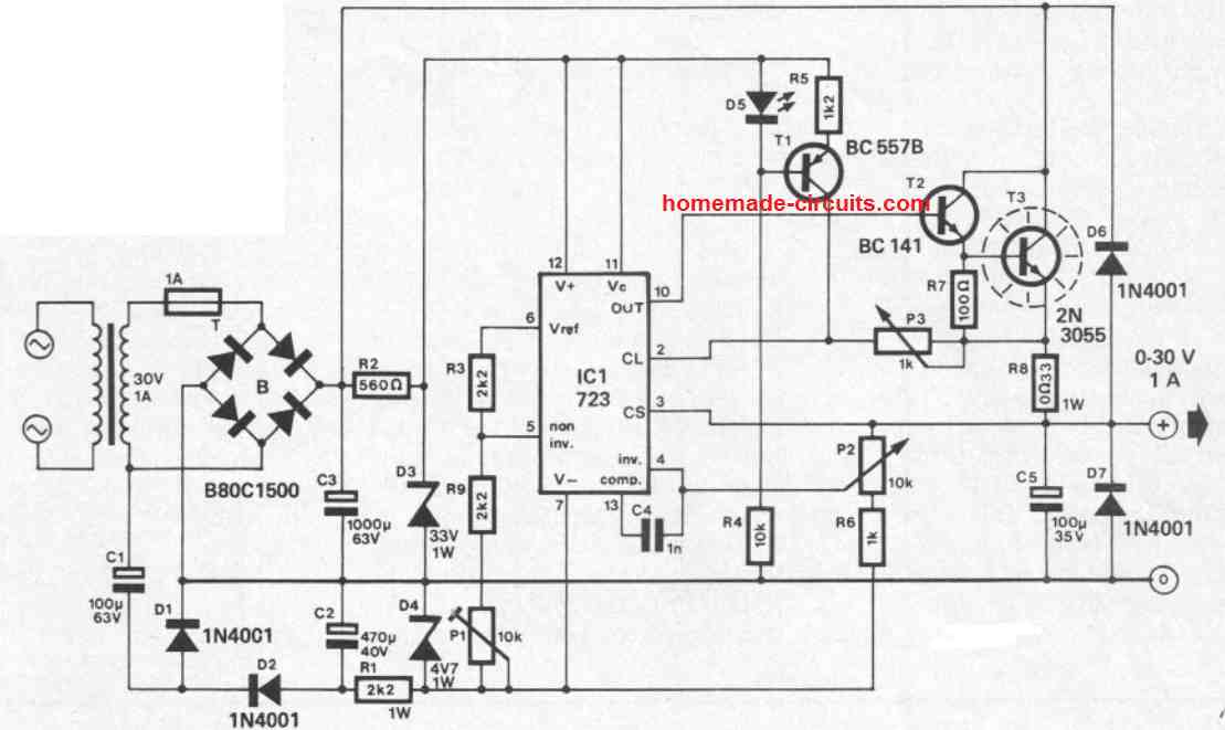
Using IC 723
The next design shows a simple yet extremely useful laboratory power supply using the IC LM723:
Hello Swagatam
congratulations good diagram
Laboratory Power Supply Circuit,
As it is the show do your job
R17
R18 himself encuantra along with S2
Some proble if I eliminate what’s mentioned is stops
Joining the To
I am modifying the diagram for 30V – 10A
You would spend me if you publish a diagram of
Station of digital solder
Thanks
Thanks Daniel,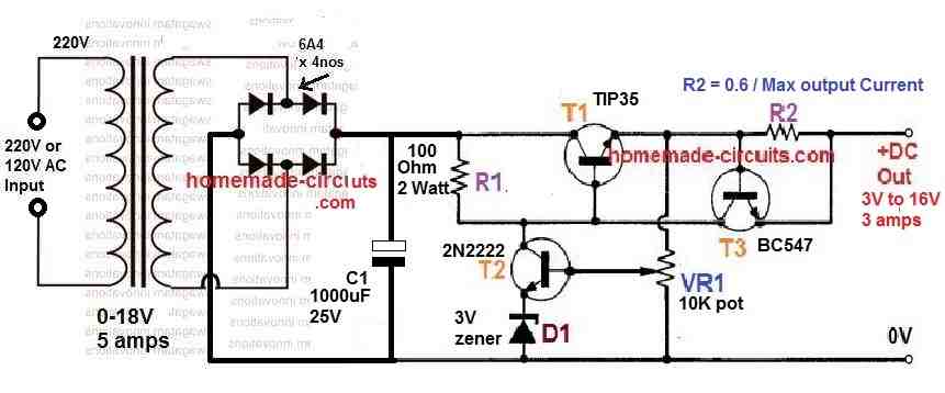
Sorry, I cannot understanding your Google translation.
However, I have a very easy and yet very nice Lab power supply which you can try. Here’s the simple version:
" rel="ugc">
For 10A you can use two TIP35 in parallel.
0 to 18v : 0 to 5 amp variable power output.input 19.5v 4.7a Sony tv power supply unit.
I want to design a transformer based power supply with Stabilized voltage output having the following specifications:
Vout = 0 – 400 volts
Iout = 0 – 150mA. Getting the transformer is not a problem. How can I design the circuit using lm317 or any better linear voltage regulator, pass transistors, opamps and mosfet to achieve that. I am looking forward to having this achieved through you or a link of previous work done in similar area. Thanks.
You can try the following concept, but there is no adjustable current control. Current is through a fixed resistors. The input series lamp is not required when a transformer is used.
https://www.homemade-circuits.com/0-300v-variable-voltage-current/
Thanks you sir.i have built this circuit you sent me in both transformer less and transformer based and they are working fine but their out voltages are not Stabilized. That is why am seeking for a design that will incorporate lm317 linear regulator and opamps for constant voltage output regardless of the current provided it is within 0 -150mA.
Hi Mosses, I understand, but LM317 IC or opamps cannot be used with 400 V potentials, that’s the problem.
The design which I suggested can be used to produce selected fixed stabilized output voltages if the mosfet gate potentiometer is replaced with zener diode.
Hi Swagatam,
My last comment was about the 1st circuit.
I’ve noticed that the circuit is incomplet.
There’s a mention of IC3 but there’s no such IC in the schematic.
Nélio.
Hi Swagatam,
The transformer is indicated as having 2 secondary winding of 42V by 5A, 2 secondary winding of 17V 250mA and 1 of 7V 3A.
How it is connected in the circuit?
For my understanding, this PSU is 0-50V 0-5A output.
Nélio.
Hi Nelio,
Please check out the original diagram below. I have removed many of the unnecessary things from this diagram and posted in the article:
" rel="ugc">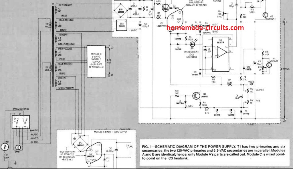
what if we Use a pot of 20 K or 50 k in LM 723 circuit ‘ for Adjust the output voltage
It will work, but it will cause the full scale range to be completed at the mid way of the pot adjustment.
Hi, do you have a link to the original article on the second schematic “Another Simple Laboratory Power Supply Circuit using LM324 IC” or perhaps a copy of it?
Rhanks, Mac
Hi, It was contributed by a reader through comments, I do not have the original link.
Ok thank you.
Mac
Saudações, senhor Swagatam.
adquiri todos os componentes desta incrível fonte.
Usarei no lugar do LF357 o LF356(genuíno).
Acredito que o LF 356
*(não achei o LM357 ! venda no meu país, se não, os fakes)*
funcionará bem.
Por via das dúvidas, comprei também o LM301AN(genuíno).
Gratidão desde já.
Att, Luís Carlos Marques
Greetings, Mr Swagatam.
I purchased all the components of this amazing power supply.
I will use instead of LF357 the LF356(genuine).
I believe the LF 356
*(I didn’t find the LM357 ! sell in my country, if not, the fakes)*
will work fine.
Just in case, I also bought the LM301AN(genuine).
Gratitude in advance.
Att, Luís Carlos Marques
Thank you Luis, for the update! I wish you all the best! I Hope you are able to succeed with the project!
Dear Sir Swagatam.
Thanks in advance for the design of this power supply with the LM330k, LF357 and MJ15023.
After researching, I came to the conclusion, this is the best project.
I will build.
Thank you Luis, I am glad you liked the post!
Sir engineer Swagatam
Hello dear. You are certainly aware that produced gases during soldering action are harmful for our lungs and eyes. To prevent inhaling it, I have been using a 200 mA, 12V Fan, feeding with a 220 to 15 v transformer that is regulated with a LM7812 IC. during few years ago. Last month, I added a dimmer before the primary of transformer to reduce the speed of the fan and the result was interesting: I get 12 Volts DC output with 60 Volts AC (after dimmer) and 6 volts DC with 30 volts. in other words, DC voltage changes between 6 and 12 volts when AC voltage after dimmer changes from 30 to 60 volts. I want you to please do a favor and tell me What is your idea about using this method (with or without 7812 and other regulator ICs, of course) to get variable voltage instead of other circuits which use LM317, transistors, and etc. If there is no problem, would you please design a similar variable 0 to 35 V power supply circuit for your eager visitors?
Best regards
Mike
Hi Mike,
A 7812 IC is supposed to give you a constant 12V regardless of the input fluctuation, unless the input drops below 13V.
Whether it is a 7812 based circuit, or a LM317/LM338, or a transistorized regulator, all these are linear regulators, and are prone to heating up when the input/output difference rises beyond a certain range.
If you are OK with the heat dissipation, then you can try investigating the following two posts:
Voltage Regulator Circuits using Transistor and Zener Diode
How to Design a Bench Power Supply Circuit
If you prefer a buck converter based regulator for ensuring minimum heat dissipation, then probably you can try the following concept:
LM317 Variable Switch Mode Power Supply (SMPS)
Dear Sir Engineer Swagatam
Hello.Thank you so much for proposing these very useful posts.
Truly yours
Mike
You are most welcome Mike!
This circuit diagram is not correct.Control in to pin 7 is not correct it is a Vcc Pin
It was taken from one of the reputed magazines, it seems the pin7 must go directly to the OUT pin of the LM317…
I’ve just compared my schematic to yours and mine is the correct circuit, with pin 7 connected to the OUT line and the bottom of R14 connected to pin 2.
OK thanks for the information
I am busy designing a pcb for this circuit and the pcb foil given in the original article is correct, it has R14/C7 connecting to pin 2 of the IC. This is really just a tweaked version of the circuit in the datasheet of the LM350, for the 5a constant voltage/current regulator.
OK that sounds great, but please remember that this design was taken from one of the magazines and it has not been verified by me personally…..
Hello, Mr. Swagatan.
I have almost all the components of the design of this power supply.
LM338K (Original).
transformer 24 volts x 5A + 12 + 12v x 500mA.
The problem that makes me afraid is Oamp LF357. Here in Brazil I don’t think so.
Which one should I replace without having to calculate the current circuit?
(Someone quoted the AD825).
Thank you very much.
Hugs, Luís.
That sounds great Luis.
I am sure that a 741 IC will also work equally well instead of the LF357. Because the basic idea of the op amp is to compare the voltages at its input and execute. The LED at pin6 is very important as it will block any offset voltage that the 741 may have across its output so make sure to include that LED.
You can try AD825, LM321, or ultimately 741
Hello Swagatam,
greetings to you.
I have a 24v 0 24v 5amps transformer and would like to use the above circuit to make a Bench power supply, would you recomend the above or you have some alternatives, kindly suggest.
warm regards
Patrick
Hi Patrick, the above circuit is not good, I have plenty of good ones with me, I’ll try to update them soon in the above article, for your reference
Dear Swagatam,
Thankyou, waiting eagerly.
Reagards
Thanks Patrick,
Could you please specify the maximum voltage and current range that you intend to have in your bench power supply
Hello Swagatam,
I will rephrase my question, I have a 24 0 24v 5amps Transformer, what is the best Bench Power supply I can build with it.
thank you for all the support,
warm regards
Thank you Patrick, actually I have to manage the comments from a different page which does not allow me to see the earlier comments, and therefore I could not access to your previous comments .
No problem, you can probably try the last circuit from the following post, which will to a great extent solve your requirement…
https://www.homemade-circuits.com/lm317-with-outboard-current-boost/
I actually have many versions of bench power supplies, but most of them are complex and include a huge number of discrete parts, therefore I thought it’s better to go for an LM317 based design with adjustable voltage and current features.
Swagatam,
There is a BR3 shown in the parts lists but no BR3 I can find in either the circuit diagram or the PCB layout. This design and instruction is missing a good bit of necessary detail.
Can you please advise on the above.
Rob, the original diagram had another IC1, Q1, Q2 identical stage for enabling a dual supply at the output. BR3 represented the bridge rectifier for this circuit.
This would explain why the transformer is rated for 600VA and has (2) 42V & (2) 17V volt secondaries (I think)? Please confirm but I believe this would mean, if one only follows the provided circuit diagram, that only a 300 VA (50V * 5A = 250W ~300 VA) transformer is required?
The T1 Quintuple Transformer suggested in the above parts list would not be a cheap item and 42V secondary outputs with 120VAC primaries are difficult to source in the USA.
Alternatively, if I elected to do a dual-output design (i.e. doubling IC1, Q1 & Q2) basically the entire circuit should be duplicated, correct? In other words two separate PCB’s as shown above (one for each output) with no common circuit elements. Basically, two entirely separate and independent power supplies with only the transformer (T1) being shared? Do I have this correct?
Yes, that’s correct. For dual supply the entire design presented in the above article must be replicated by assembling over a separate identical PCB. In addition to this the original diagram also had a separate 5 V 5 amp fixed voltage regulator circuit, as shown below:
Swagatam,
For the Panasonic capacitors you have given models P6430, P6272 & P6420. These items appear to be Polypropylene Film Capacitors and are obsolete. Can you please clarify the required capacitor type and other details or confirm any capacitor with the required capacitance and rated voltage is sufficient.
I’m assuming for all capacitor voltage ratings ‘volts’ should be taken as VDC. Please clarify if this assumption is not correct.
Is there any minimum requirement on Capacitor tolerance or is +/-20% acceptable.
Finally, for IC2 and the LF357A JFET, there exists an LF3578A… from various manufacturers but no LF357A specifically. Can you please clarify the IC required? Thanks in Advance!
Rob, The rule of thumb for capacitors is that the voltage rating should be two times more than the Vcc. PPC are the best, although disc ceramic should also be fine.
I have no idea about LF3578A and I cannot find its datasheet either…I think the op amp is not critical, an ordinary IC 741 should also work
Swagatam,
Thanks for your help with this.
Below is a link to the Texas Instruments LM3578A 8-PIN Switching Regulator:
https://www.ti.com/product/LM3578A
After some searching it appears the LF357 is mostly obsolete:
As I am new to electronics so it is not clear to me if the extra letter designations in these integrated Circuit ‘Types’ are significant? In other words, will a LF357A perform like LF357 or LF357M/NOPB?
Anyway, after some research I believe the following alternatives might be adequate to replace the LF357(A):
TL071CDT from ST Microelectronics:
https://www.st.com/content/st_com/en/search.html#q=LF357-t=x-reference-page=1
TLE2071, TLE2081 & OPA637 from Texas Instruments:
https://e2e.ti.com/support/amplifiers/f/14/t/84056?keyMatch=LF357&tisearch=Search-EN-everything
No problem Rob, The LM3578 is a switching regulator, whereas the LM357A is an op amp, so LM3578 cannot be used here.
Any other similar variant should work, like the mentioned TL071 etc which are op amps.
You can also try IC 741, M321, or LM358 according me, all of these should be able do the job well.
Can you please provide downloadable files for the circuit schematic, parts list & PCB layout.
The circuit schematic cuts off the 120VAC input.
If they already exist the eagle/gerber files for the PCB layout would be appreciated.
I am sorry, I am do not have the designs in the downloadable format at this moment.
Hello sir,
I would like to know, how did you calculate the stability of your power supply’s circuit?
I’ve been trying to design my own power supply using discrete components but I do not know how to find the stability of it.
Hello Anurag, the circuit relies on the IC LM317 which itself is a highly stabilized device, and therefore the output from the circuit will be also highly stabilized
I need to make a 13.8 V, 25A power supply(adjustable) using this circuit , What are the changes I have to make? Please help
.
you will have to add many more Q1, Q2 stages until they all together reach the 25 amp capacity, or you can try the following concept:
https://www.homemade-circuits.com/make-25-amp-solar-battery-charger-power/