In this post I have explained 9 LDR circuit projects that uses LDR light sensor to trigger a load ON/OFF through a relay. These circuits are mostly triggered by the absence or the presence of light on the LDR. The circuits are built using transistors, op amps and LDR along with a switching relay. Let's find out more.
As the name suggests an LDR or Light Dependent Resistor is a kind of resistor that exhibits a wide range of resistance values depending on the intensity of light incident on its surface. The variation in the resistance range can be anywhere from few hundred ohms to many megaohms.
They are also known as photoresistors. The resistance value in an LDR is inversely proportional to the intensity of the light falling on it. Meaning when the light is less, the resistance is more and vice versa.
LDR Internal Construction
The following figure shows the internal dissected view of an LDR device wherein we can see the photoconductive substance applied within the zig zag or coiled pattern, embedded over a ceramic insulating base, and with the end points terminated as leads of the device.
The pattern ensures maximum contact and interaction between the crystalline photoconductive material and the electrodes separating them.

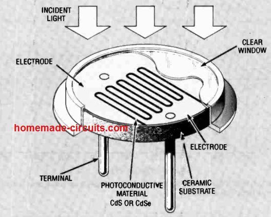
The photoconductive material generally consists of cadmium sulfide (CdS) or cadmium selenide (CdSe).
The type and thickness of the material and width of its deposited layer specify the range of the LDR resistance value and also the amount of watts it can handle.
The two leads of the device is embedded within an an opaque non-conductive base with an insulated transparent coating over the photo-conductive layer.
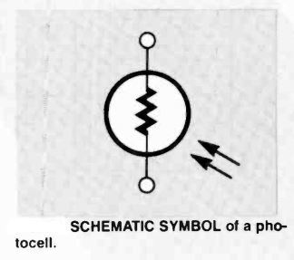
The schematic symbol of an LDR is shown below:
LDR Sizes
The diameter of photocells or LDRs may range from 1/8 inch (3 mm) to above one inch (25 mm). Commonly these are available with diameters of 3/8 inch (10 mm).
LDRs smaller than this are generally used where space may be a concern or in SMD based boards. The smaller variants exhibit lower dissipation. You may also find a few variants that are hermetically sealed to ensure reliable working even under harsh and undesirable environments.
Comparing LDR Characteristics with Human Eye
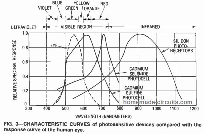
The graph above provides the comparison between the characteristics of photosensitive devices and our eye. The graph shows the plotting of Relative spectral response against wavelength from 300 to 1200 nanometers (nm).
The human eye characteristic waveform indicated by the dotted bell shaped curve reveals the fact that our eye has enhanced sensitiveness to a relatively narrower band of the electromagnetic spectrum, approximately between 400 and 750 nm.
The peak of the curve has a maximum value in the green light spectrum within the range of 550 nm. This stretches down into the violet spectrum having a range between 400 to 450 nm on one side. On the other side this extends into the dark red light region having a range between 700 to 780 nm.
The figure above also reveals exactly why cadmium sulfide (CdS) photocells tend to be the favorites in light-controlled circuit application: the spectral response curve peaks for Cds is near 600 nm, and this specification is quite identical to the range of human eye.
In fact, the cadmium selenide (CdSe) response curve peaks may even extend beyond 720 nm.
LDR Resistance Vs Light Graph
That said CdSe may exhibit higher sensitivity to almost the whole range of the visible-light spectrum. In general the characteristic curve of a CdS photocell may be as given in the following figure.
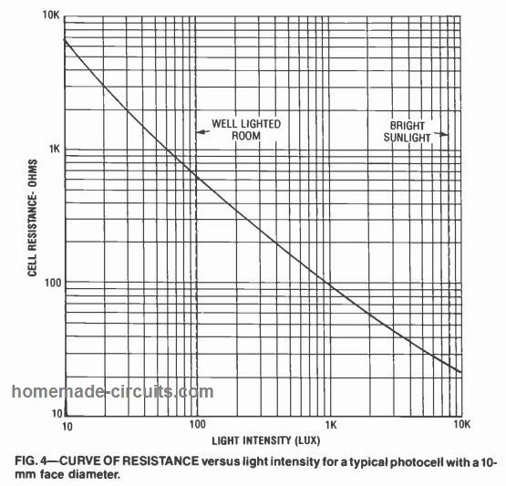
Its resistance in the absence of light can be around 5 megohms, which may drop to around 400 ohms in the presence of light intensity of of 100 lux or a level of light equivalent to an optimally illuminated room, and around 50 ohms when the light intensity is as high as 8000 lux. typically as obtained from a direct bright sunlight.
The lux is the SI unit for illuminance generated by a luminous flux of 1 lumen evenly spread over a surface of 1 square meter. The modern photocells or LDRs are adequately rated for power and voltage, at par with normal fixed type resistors.
The power dissipation capacity for a standard LDR could be around 50 and 500 milliwatts, which may depend on the quality of the material used for the detector.
Perhaps the only thing not so good about LDRs or photoresistors is their slow response specification to light changes. Photocells built with Cadmium-selenide typically exhibit have shorter time constants than cadmium-sulfide photocells (approximately 10 milliseconds in contrast to 100 milliseconds).
You may also find these devices having lower resistances, increased sensitivity, and elevated temperature resistance coefficient.
The main applications in which Photocells are normally implemented are in photographic exposure meters, light and dark activated switches for controlling street lights, and burglar alarms. In some light activated alarms applications the system is triggered through a light beam interruption.
You may also come across reflection based smoke alarms using photocells.
LDR Applications Circuits with Diagrams
The following images shows a few of the interesting practical photocell application circuits.
1) Light Activated Relay
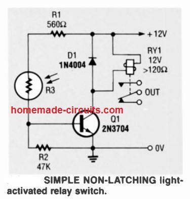
The first straightforward LDR circuit project indicated in the above diagram is built to respond whenever light falls on the LDR installed into a normally dark cavity for example the inside a box or housing.
The photocell R1 and resistor R2 create a potential divider that fixes the base bias of Q1. When it is dark, the photocell exhibits an increased resistance, leading to a zero bias on the base of Q1, due to which, Q1 and the relay RY1 remain switched off.
In case an adequate level of light is detected on the photocell LDR, its resistance level quickly falls to some lower magnitudes. and a biasing potential is allowed to reach the base of Q1. This switches ON relay RY1, whose contacts is used to control an external circuit or load.
2) Darkness Activated Relay
The second LDR project shows how the first circuit can be transformed into a darkness activated relay circuit.
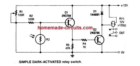
In this example the relay activates in the absence of light on the LDR. R1 is used for adjusting setting up the sensitivity of the circuit. Resistor R2 and the photocell R3 work like a voltage divider.
The voltage at the junction of R2 and R3 rises when light falls on the R3, which is buffered by emitter follower Q1. The emitter output of Q1 drives common emitter amplifier Q2 via R4, and correspondingly controls the relay.
3) Precision LDR Light Detector
Although simple, the above LDR circuits are vulnerable to supply voltage changes and also ambient temperature changes.
The 3rd circuit diagram below shows how the drawback could be tackled through a sensitive-precision light activated circuit that would work without getting affected from voltage or temperature variations.
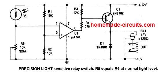
In this circuit the LDR R5, pot R6, and resistors R1 and R2 are configured with each other in the form of a Wheatstone bridge network.
The op amp ICI along with the transistor Q1 and relay RY1 work like a very sensitive balance detecting switch.
The balancing point of the bridge does not get affected, regardless of variations in the supply voltage or the atmospheric temperature.
It is only effected by the changes in the relative values of the components associated with the bridge network.
In this example the LDR R5 and pot R6 constitute one arm of the Wheatstone bridge. R1 and R2 form the second arm of the bridge. These two arms act like voltage dividers. The R1/R2 arm establishes a constant 50% supply voltage to the non-inverting input of the op-amp.
The potential divider formed by the pot and the LDR generates a light dependent variable voltage to the inverting input of the op amp.
The setting up of the circuit, pot R6 is adjusted so that the the potential at the junction of R5 and R6 goes higher than the potential at pin3 when the desired amount of ambient light falls on the LDR.
When this happens the output of the op amp instantly changes state from positive to 0V, switching ON Q1 and the attached relay. The relay activates and switches OFF the load which could be a lamp.
This op amp based LDR circuit is very precise and will respond even to minute changes in light intensities, which cannot be detected by human eye.
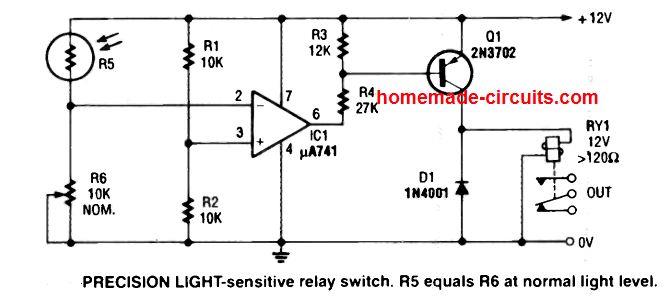
The above op amp design can be easily transformed into a darkness activated relay either by swapping the pin2 and pin3 connections, or by swapping the R5 and R6 positions, as demonstrated below:
4) Adding Hysteresis Feature
If required this LDR circuit project can be upgraded with a hysteresis feature as shown in the 4rth diagram below. This is done by introducing a feedback resistor R5 across the output pin and the pin3 of the IC.
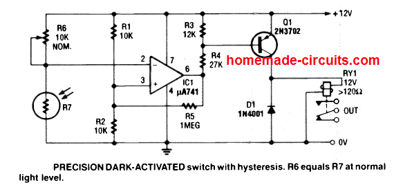
In this design the relay actuates normally when the light intensity goes above the preset level. However when the light on the LDR drops and decreases than the preset value, it does not switch OFF the relay due to the hysteresis effect.
The relay switches OFF only when the light has dropped to a significantly lower level, which is determined by the value of R5. Lower values will introduce more delay lag (hysteresis), and vice versa.
5) Combining Light and Dark Activation Features in One
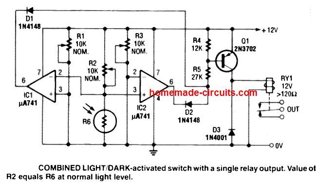
This 5th design is a precision light/dark relay is designed by combining the previously explained dark and light switch circuits. Basically it's a window comparator circuit.
The relay RY1 is switch ON when either the light level on the LDR surpasses one of the pot setting or drops below the other pot setting value.
Pot R1 determines the darkness activation level, while the pot R3 sets the threshold for the light level activation of the relay. The pot R2 is used for adjusting the supply voltage to the circuit.
The setting up procedure includes adjusting the first preset pot R2 such that approximately half supply voltage is introduced at the LDR R6 and pot R2 junction, when the LDR receives light at some normal intensity level.
Potentiometer R1 is subsequently adjusted such that relay RY1 switches ON as soon as the LDR detects a light below the preferred darkness level.
Likewise, pot R3 can be set up so that the relay RY1 is switched ON at the intended brightness level.
6) Light Triggered Alarm Circuit

Now let's see how an LDR can be applied as a light activated alarm circuit as explained in this 6th circuit design.
The alarm bell or buzzer should be intermittent type meaning sounding with an continuous ON/OFF repetitions, and rated to work with current less than 2 amp. LDR R3 and resistor R2 make a voltage divider network.
Under low light conditions, the photocell or LDR resistance is high which causes the voltage at R3 and R2 junction insufficient to trigger the attached SCR1 gate.
When the incident light is brighter, the LDR resistance drops to a level sufficient to trigger the SCR, which turns on and activates the alarm.
Oppositely when it gets darker, the LDR resistance increases, switching OFF the SCR and the alarm.
It is important to note that the SCR here turns OFF only because the alarm is an intermittent type which helps to break the latch of the SCR in the absence of a gate current, shutting off the SCR.
7) Adding a Sensitivity Control
The above SCR LDR alarm circuit is quite crude and feature very low sensitivity, and also lacks a sensitivity control. The 7th figure below reveals how the design could be enhanced with the mentioned features.
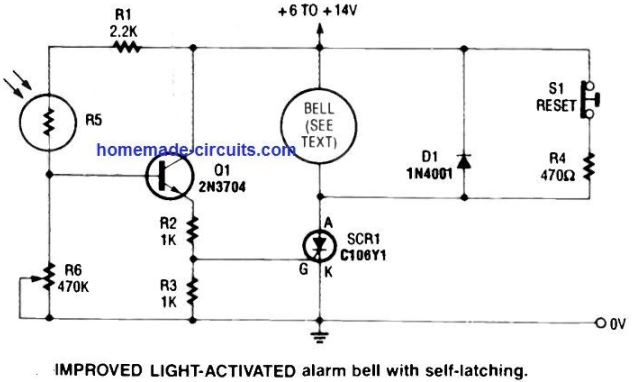
Here, the fixed resistor in the previous diagram is replaced with a pot R6, and a buffer BJT stage introduced through Q1 between the gate of the SCR and the LDR output.
Additionally, we can see a push to off switch A1 and R4 parallel to the bell or the alarm device. This stage allows the user to convert the system into a latching alarm regardless of the intermittent nature of the bell device.
The resistor R4 ensures that even while the bell rings in an self interrupting sound, the latching anode current never breaks and the SCR remains latched once triggered ON.
S1 is used to break the latch manually and shut down the SCR and the alarm.
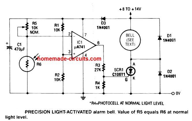
In order to further enhance the above explained SCR light activated alarm with improved precision, an op amp based triggering can be added as shown below. The working of the circuit is similar to the previously discussed LDR light activated designs.
8) LDR Alarm Circuit with Pulsed Tone Output
This 8th concept is yet another dark activated alarm circuit featuring an integrated a low power 800 Hz pulse generator for driving a loud speaker.
Referring to the circuit diagram below we can see two NOR gates IC1-c and ICI-d are configured as an astable multivibrator for generating a frequency of 800 Hz. This frequency is fed into the speaker via a small signal amplifier using the BJT Q1.
The above NOR gate stage is activated only as long as the output of IC 1-b becomes low or 0V. The other two NOR gates IC 1-a and IC1-b are similarly hooked up as astable multivibrator for producing a 6 Hz pulse output and is also enabled only when the gate pin 1 is pulled low or at 0V.
Pin1 can be seen rigged with the potential divider junction formed by the LDR R4 and pot R5.
It works like this: When the light on the LDR is sufficiently bright the junction potential is high, which keeps both the astable multivibrators disabled, which means no sound output from the loudspeaker.
However when the light level drops below the preset level, the R4/R5 junction gets sufficiently lower which activates the 6 Hz astable. This astable now begins gating or switching the 800 Hz astable at 6 Hz rate. This results in a multiplexed 800 Hz tone on the speaker, pulsed at 6 Hz.
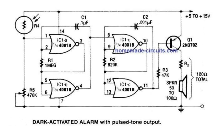
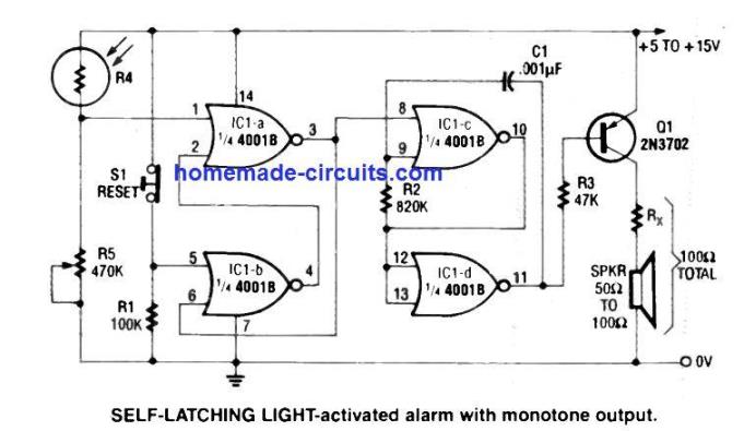
To add a latching facility to the above design, just add the switch S1, and the resistor R1 as given below:
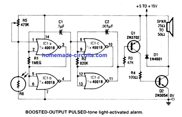
For getting a loud, boosted sound from the speaker, the same circuit can be upgraded with an enhanced output transistor stage as shown below:
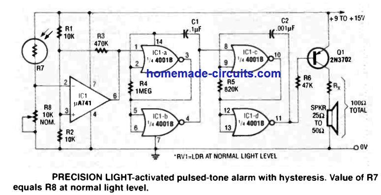
In our earlier discussion I have explained how an op amp can be used for enhancing the LDR light detection precision. The same can be applied in the above design to create a super precision pulse tone light detector circuit
9) LDR Burglar Alarm Circuit
A simple LDR light beam interruption burglar alarm circuit can be seen in the 9th circuit diagram below.
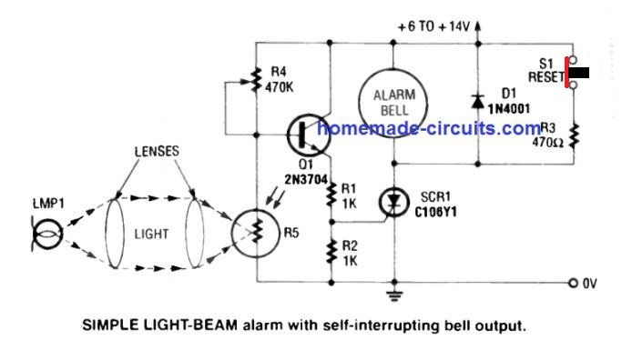
Normally, the photocell or the LDR receives the required amount of light through the installed light beam source. This can be from a laser beam source also.
This keeps its resistance is low and this also produces insufficiently low potential at the pot R4 and photocell R5 junction. Due to this the SCR along with bell remain deactivated.
However, in an event the light beam gets interrupted causes the LDR resistance to increase, significantly raising the junction potential of R4 and R5.
This immediately triggers the SCR1 switching ON the alarm bell. Resistor R3 in series with switch S1 are introduced to enable permanent latching of the alarm.
Summarizing LDR Specifications
There are many different names by which the LDR (Light Dependent Resistors) are known, which include names such as photoresistor, photocell, photoconductive cell, and photoconductor.
Normally the term which is most prevalent and used most popularly in instructions and the datasheets is the name “photocell”.
There are a variety of uses to which the LDR or photoresistor can be applied since these devices are good with their photosensitive property and are also available at low cost as well.
Thus, LDR could remain popular for a long period of time and extensively used in applications such as photographic light meters, burglar and smoke detectors, in street lamps to control the lighting, flame detectors, and card readers.
The generic term of “photocell” is used for the Light Dependent Resistors within the general literature.

Discovery of LDR
As discussed above, the LDR has remained the favorite among the photocells for a long period of time. The early forms of the photoresistors were manufactured and introduced in the market in the early nineteenth century.
This was manufactured through the discovery of the “selenium’s photoconductivity” in 1873 by the scientist named Smith.
A good range of different photoconductive devices have been manufactured since then. An important progress in this field was made in the early twentieth century, especially in 1920 by the renowned scientist T.W. Case who worked on the phenomenon of photoconductivity and his paper, “Thalofide Cell- a new photoelectric cell” was published in 1920.
During the next two decades in the 1940s and 1930s, a range of other relevant substances were studied for developing photocells which included PbTe, PbS, and PbSe. Further in 1952, the photoconductors the semiconductor version of these devices were developed by Simmons and Rollin using germanium and silicon.
Symbol of the Light Dependent Resistors
The circuit symbol which is used for the photoresistor or the light dependent resistor is a combination of the resistor animated to indicate that the photoresistor is light sensitive in nature.

The basic symbol of the light dependent resistor consists of a rectangle which symbolizes the resistor's function of the LDR. The symbol additionally consists of two arrows in the incoming direction.
The same symbol is used to symbolize the sensitivity towards light in the phototransistors and photodiodes.
The symbol of the “resistor and arrows” as described above is used by the light dependent resistors in majority of their applications.
But there are few cases where the symbol used by the light dependent resistors depicts the resistor encased within a circle. This is evident in the case when circuit diagrams are drawn.
But the symbol where there is absence of circle around the resistor is a more common symbol used by the photoresistors.
Technical Specifications
The surface of LDR is built with two cadmium sulphide(cds) photoconductive cells having spectral responses comparable to that of the human eye. The resistance of the cells drop linearly as light intensity is increased on its surface.
The photoconductor which is placed between the two contacts is used as a main responsive component by the photocell or the photoresistor. The resistance of the photoresistors undergoes a change when there is an exposure of the photoresistor to the light.
Photoconductivity: The electron carriers are generated when the photoconductor’s semiconductor materials used absorb the photons, and this results in the mechanism which works behind the light dependent resistors.
Although you may find that the materials which are used by the photoresistors are different, they are mostly all semiconductors.
When they are used in the form of photoresistors, then these materials act as resistive elements only where there is absence of PN junctions. This results in the device to become entirely passive in nature.
The photoresistors or the photoconductors are basically of two types:
Intrinsic Photoresistor: The photoconductive material which is used by a specific photoresistor type enables the charge carriers to get excited and jump to the conduction bands from their initial valence bonds respectively.
Extrinsic Photoresistor: The photoconductive material which is used by a specific photoresistor type enables the charge carriers to get excited and jump to the conduction bands from their initial valence bonds or impurity respectively.
This process requires non-ionized impurity dopants which are also shallow and requires this to take place when light is present.
The design of the photocells or extrinsic photoresistors is done specifically considering the long wavelength radiations such as the infra-red radiations in most of the cases.
But the designing also considers the fact that any type of thermal generation needs to be avoided since they are required to operate at temperatures which are very relatively low.
Basic Structure of LDR
The number of natural methods which are commonly observed for the manufacturing of the photoresistors or the light dependent resistors is very few in number.
A resistive material sensitive to light is employed by the light dependent resistors for constant exposure to light. As discussed above, there is a specific section which is processed by the light sensitive resistive material which is required to be in contact with both or one of the ends of the terminals.
A semiconductor layer which is active in nature is used in a general structure of a photoresistor or a light dependent resistor and an insulating substrate is further used for depositing the semiconductor layer.
In order to provide the semiconductor layer with the conductivity of the required level, the former is doped lightly. Thereafter, terminals are connected appropriately across the two ends.
One of the key issues in the basic structure of the light dependent resistor or photocell is its material’s resistance.
The contact area of the resistive material is minimized to ensure that when the device is exposed to the light, it undergoes a change in its resistance efficiently. In order to achieve this state, it is ensured that surrounding area of the contacts is doped heavily which results in the reduction of the resistance in the given area.
The shape of the surrounding area of the contact is designed to be mostly in the interdigital pattern or the zig zag form.
This enables the maximization of the exposed area along with the reduction in the levels of the spurious resistance which in turn results in the enhancement of the gain by contracting the distance between the two contacts of the photoresistors and making it small.
There is also a possibility of the usage of the semiconductor material such as polycrystalline semiconductor depositing it on a substrate. One of the substrates which can be used for this is ceramic. This enables the light dependent resistor to be of low cost.
Where Photoresistors are Used
The most attractive point of the light dependent resistor or a photoresistor is that it is of low cost and thus is widely used in a variety of electronic circuit designs.
Apart from this their rugged features and simple structure also provides them with an advantage.
Although the photoresistor lacks various features which are found in a phototransistor and a photodiode, it is still an ideal choice for a variety of applications.
Thus, LDR has been continuously used for a long period of time in a range of applications such as photographic light meters, burglar and smoke detectors, in street lamps to control the lighting, flame detectors, and card readers.
The factor which determines the photoresistor properties is the material type which is used and thus the properties can vary accordingly. Some of the materials used by the photoresistors possess constants of very long time.
Thus, it is quintessential that the photoresistor type si selected carefully for specific applications or circuits.
Wrapping up
Light dependent resistor or LDR is one of the very useful sensing devices which can be implemented in many different ways for processing light intensity. The device is cheaper compared to other light sensors, yet it is able to provide the required services with utmost efficiency.
The above discussed LDR circuits are just a few examples which explains the basic mode of using an LDR in practical circuits. The discussed data can be studied and customized in several ways for many interesting applications. Have questions? Feel free to express through the comment box.

Have Questions? Please Leave a Comment. I have answered over 50,000. Kindly ensure the comments are related to the above topic.
Hi. Enjoy your website thank you.
On a breadboard I assembled 2Darkness Activated Relay and 3 Precision LDR light detector and 3 with hysteresis.
In each case the Relay chatters as light slowly changes. I’m planning on using circuit to drive some fans in my boat during daylight. I imagine the sun coming up slowly will cause the Relay to chatter. Thought the hysteresis option might stop that but no. Tried option 2 which didn’t seem to chatter but struggled to turn it into a light detector rather than dark.
Other thing is my FRT2S Relay capable of handling 400ma fan load. Where should I look on the datasheet?
Thank you Malc,
That’s the most common issue faced by all new hobbyists.
The remedy is simple, either add a small value capacitor such as a 47uF/25V capacitor right across the Base/Emitter of the relay driver transistor, or more simply add a 100uF capacitor directly across the relay coil terminals. Make sure the polarity of the capacitor is correct in both the cases.
The datasheet of your relay can be seen below:
https://www.cypax.dk/pdf/FRT2S.pdf
According to it, Contact Rating (Resistive Load) = 2A 30VDC/ 0.6A 125VAC
Let me know if you have any further doubts or questions?
Chatter has stopped. Thanks for your help.
Glad to hear that!
Hello boss.
Can you help me with simple ldr circuit diagram that can detect Human movement in darkness.
Hello Kamkooltech, LDR cannot detect a human in darkness, LDR can detect a difference in light.
You can use a doppler sensor or a PIR based circuit instead.
Thanks boss, share me some samples you have, really want to try something out
Sure, you can try the following alternative options:
https://www.homemade-circuits.com/how-to-connect-and-use-rcwl-0516-microwave-sensor/
https://www.homemade-circuits.com/pir-burglar-alarm-circuit/
Hello boss, am facing challenges here on my proteus design. I want to run a LDR project that will use 3v battery switch on multiple led.
My text error, once I use 3v the light will not bright, if I make it 6v to 9v the light will bright but it can’t switch 5,6 and more led light.
This are my materials.
Battery, 100k, 300h, BC547 and LED’s.
Please analyse it for me.
Thank you
Hello Kamkooltech, I never use softwares, so analyzing a software result may not be possible for me. However in reality if you apply 6 V or 9 V to 3V LEDs without resistors then all your LEDs would burn instantly, the transistor would also burn. A 3V should be perfectly fine for illuminating parallel connected 3V LEDs, provided the battery current is sufficiently rated to handle the LED current. For the transistor you must use 2N2222……. and where is 100K used, is it at the transistor base?…then that is too high…your LED won’t light up with a 100K base resistor.
Ok boss. Thank you so much
Dear Swagatam,
I have a need for an LDR controlled relay circuit like the one you have posted here. Unfortunately, I am stuck with a 5 volt supply, operating a 5 volt relay. Can the one you have listed be modified to operate at 5 volts? I use this design when building a 12 volt relay circuit and it does very nicely. Simple ldr circuits tried leave a lot to be desired by not being sensitive enough to light. Thanks for any help!
Hi Bob,
If you are referring to the first circuit, yes it can be operated with a 5V supply and a 5V relay. The sensitivity of the circuit can be increased by increasing the value of the R2 resistor and vice versa.
Hello my friend,
The circuit works very well with a 5 volt relay without any other changes made. I may alter R2 a bit to fine tune it, but it is very usable as is.
Thank You !
Now I have to look at all your other projects ! So many are published on the web that just do not work.. It’s great to find your site.
Bob
Thanks my Friend, I am glad it worked for you! Please keep up the good work. All the best to you!
what is nominal resistance value of a standard LDR .
It may slightly differ from LDR to LDR, but on an average the minimal resistance of an LDR can be around 10K in broad daylight (under shade)
Hi Swagatam,
What the simple way to turn-off a 220v circuit when darkness is detected?
Thanks in advance,
Hi Fabio, the first circuit from this article is the simplest of doing this:
https://www.homemade-circuits.com/how-to-make-light-activated-day-night/
hi swagatham
Thanks for giving basic information
You are welcome Suresh!
Hi sir engineer Swagatam
Hello. I congratulate you for your very interesting site and your responses to the visitors as well. would you please do a favor and tell me what will happen if I replace R5 and R1 with each other; also R2 and R6 in your project under title “Precision LDR Light Detector”. will you circuit work?
Very sincerely yours
Najeh
Thank you Najieh, yes it will work, but work in the opposite way…..the relay will click ON when darkness sets in, and will click off when dawn breaks
Kind attention Mr. swagatam
I hope that you are fine. I have 2 nos of 3k NTC and I want to ask you if it is possible to change your project under title ” Precision LDR Light Detector with hysteresis feature ” in a way that it could be used as a thermostat? I am going to put the NTC in water to active the relay as soon as the temp. increases to 44 degrees centigrade. what substitutions do you propose?
Do you think that it is a good idea that I put the NTC in a glass tube, fill it with some oil and isolate it with suitable glue or aquarium paste?
Best regards
Nassim sabaa
Hello Nassim, yes that may be possible with some modifications, you can see similar projects under the following article.
https://www.homemade-circuits.com/make-simple-refrigerator-thermostat/
Hello dear Swagatam,
Thank you so much for your feedbacks which truly make me really very glad. You are a real human, Sir!
Today, I did another test and I am sure that it would be interesting to you.
I substituted the 10 K pot with a 50 K one and when I started turning it from 50 k toward zero K at the same amount of light in my previous test , it started blinking at 17 k. I continued turning the pot and when the amount of it reduced to 14 K, it stopped blinking without the need for covering the lamp with a cloth and the lamp remained on. Do you think that there might still be a solution to solve the problem with some changes in the components or …?
Yours truly
Roya
Hello Dear Roya, there’s no need to cover the lamp with cloth, instead you just have to put the LED inside an opaque tube so that the LDR is able to see only the outside daylight and no other artificial light source or the light from the load lamp
Hello dear Swagatam, 03 15 2021
Thank you again for your feedback.I acted as you had instructed and it started blinking again; but, when I did the following, I found out the reason for the blinking at last:
I put the board on the table; attached a 60 watt Lamp that had been connected to a 1 meter long wire, to the relay; inserted the LDR into a 3 cm. black plastic hose, and bent the LDR towards me, so that there was 180 degrees difference between the lamp and LDR; I then started turning the potentiometer, and as soon as the lamp came on, it started blinking and when I put a black cloth on the lamp the blinking stopped. I concluded that the reflecting of the light on the surrounding walls must have been the reason for the blinking, which is a result of the high sensitivity of your proposed circuit. Substituting the LDR with 4 other LDRs had no effect.
In order to prove my findings, I did the aforementioned test with a similar board consisting of only 4 nos. of 2SC1815 transistors that I had purchased a few years ago; I began turning the pot and when the lamp came on it remained on without even a single blinking or the need for covering the lamp with a cloth.
I think you need to reduce the sensitivity of your circuit in order to solve the problem.
Best regards
Roya
Hello Roya, I am glad the problem is solved now…… yes obviously the light from the lam which is being controlled should never reach the LDR, otherwise the circuit may get into a infinite feedback loop, causing the lamp and the relay to go into an oscillating mode.
So the LDR must be kept totally aloof from the lamp light and it must be exposed only to the ambient day light.
Dear Mr. Swagatam
Hello and thank you for your response.
I added 10, 47, 100, 220 and 470 uf capacitors at first to the B-E of transistor, then to the relay as you had instructed but the problem still exists. I wonder why this simple circuit does not work properly. would you please take a look at it again and tell me what else I should do in order to overcome the problem?
sincerely yours
Roya
Hello Roya, It is indeed very strange, because adding a capacitor across base emitter or across the relay coil should have solved the problem immediately, I have built and tried many such circuits and could solve the relay stuttering effect simply by adding a capacitor at those places.
So the circuit is perfect, and my suggestion is also perfect.
Or there’s another option, to put the capacitor between pin2 and ground…..AND please replace R2 with a 4.7 V zener diode, an R1 with a 1K resistor
Kind attention dear Swagatam
Hello. I congratulate you for your very interesting site and your respectfully responses to the questions as well.
During10 days ago That I have assembled and tested your circuit under title ” Precision LDR Light Detector ” with and without Hysteresis, I have not been able to find out the reason why the lamp that I have added to the Relay of the circuit in order to have light at our yard during the night, starts blinking for a few minutes as soon as the amount of light reduces to the amounts that I have set by variable R6 ( after the sun sets ). Blinking stops after about 5 minutes and the lamp remains on until the morning. I have changed 741 and 2N3702 with new ones for the third time but the problem still exists. I assure you that all components are healthy.
I think you are the only man who can solve my problem and makes me happy.
Best regards
Roya Shirazi
Thank you Roya for trying this project.
The relay chattering can be simply stopped by adding any capacitor between 10uF/25V and 100uF/25V, across the base emitter of the PNP transistor, or in parallel with the relay coil.
Need the spec & detaiis of parts & circuits with 5 volt supply for solarpv cell unit
For which application do you need it!
Hi Swagatam,
I have a 120vac photocell on some outside lights and on cloudy days the lights burn all day and all night. I researched several replacements and they all operate about the same, so I came up with a circuit to turn on a LED at twilight and be off at bright sunlight and be off at very dark. I am going to place it to shine on the 120vac photocell to keep the outside light off except when it is actually dark. I had a circuit with two transistors and a mosfet for light activated and a similar for dark activated LEDs so I married the two circuits together and on the breadboard a shadow will turn the LED on and greater darkness will turn the LED off. Also, the LED is off with bright light. I can’t attach the circuit here, so I am sending you an email with the circuit. I’m sure there is a lot wrong with the married circuit, so maybe you could look it over and advise me. Thanks!
Hi Norman, I don’t think this should be difficult at all, to make the relay switch OFF at almost total darkness. There should be an adjustment in all such circuits which could be appropriately set for enabling the relay to click only at the desired high darkness level. The op amp circuit in the above article is a good example which will allow this type of precise settings as per user preference.
Hi Swagatam,
The latest 555 power on delay is not causing any hum on the CK9561. The only transistor is from Pin 1 of the LM358 opamp which is used to ground the CK9561. The 555 takes up a little more room on the PCB but for this type circuit, it seems to be a superior design. The timing and sound are very clear. My second post describes the 555 design I am using. I may try to fit to caps in parallel to increase the delay time. You make me so happy with your quick responses. No one else on the net has your work ethic. Thanks!
Thank you Norman, it is probably a monostable circuit that you have built. The RC components decide the timing output of the monostable. You can refer to the following articles for the required formulas an calculations:
https://www.homemade-circuits.com/interesting-timer-circuits-using-ic-555-explored/
https://www.homemade-circuits.com/timer-ic-555-explained/
https://www.homemade-circuits.com/ic-555-timer-monostable-circuit-calculator-software/
High Swagatam,
I found a circuit on the internet that uses a 555 timer as follows: Pin 1 is grounded. Pin 4 and Pin 8 are 5v. Pin 2 and Pin 6 are shorted together. A 47K resistor connects Pin2/6 to ground. 5v is connected to the + side of an electrolytic capacitor with the negative of the capacitor connected to Pin 2/6. It works great. I breadboarded it with a 330uF electrolytic capacitor which give me a delay of about 17 seconds. I would like a little longer delay, but the largest SMD capacitor I have is a tantalum capacitor of 330uF. Is there a way to increase the delay, say to 25 seconds using this circuit with my capacitor limitations. I am using SMD components to make the PCB as small as possible.
Hi Swagatam,
I am trying to design a circuit that will trigger a CK9561 alarm chip. I want the circuit to trigger based on light. Say the alarm module is placed in a drawer and when someone opens the drawer, the alarm sounds. I need the circuit to have a power on delay so the alarm doesn’t sound when you first turn on the power, so you have time to place it in the drawer and close it so the alarm module is in complete darkness and doesn’t trigger. I am using 3v battery supply. I have used a LM358 opamp and a LDR. This works good. I have tried several power on delays with mixed success. They all allow a small amount of voltage/current to make the CK9561 chip hum or squeal lowly. I have tried your delay on timer using transistors, resistors and capacitor. I have tried 555 delay timer. They all work, but I still get the hum from the CK9561 which gets louder just before the chip fully triggers. Thanks!
Hi Norman, did you confirm the leakage by measuring it with a multi-meter? you can also try adding a high value filter capacitor across the delay timer output terminals which supplies the DC to the CK9561, and check if that stops the humming
Love Diagrams and all about them !