In this post we are going to take a look at the popular LM 324 IC. We will be looking at the pin configuration, its important features and its technical specifications and finally we will be looking at some of the fundamental application circuits using LM 324.
If you are looking for a low voltage operational amplifier (3V and above) IC which can work on single and dual power supplies with wide range of frequencies and with minimal power consumption, then LM324 can be the best suited for your design. It is available as THT or through hole technology and SMD or surface mound device packages.
Now let’s look at the key features:
Main Features
• It can operate from 3 V to 30 V single power supply.
• It can operate from +/- 1.5 V to +/- 15 V for dual supply.
• It has bandwidth up to 1.3 MHz
• Large voltage gain of 100 dB
• 4 independent amplifiers.
• Some of the variants are short circuit protected at the output.
• True differential input stages.
• Very low current consumption: 375 uA.
• Low input bias current: 20 nA.
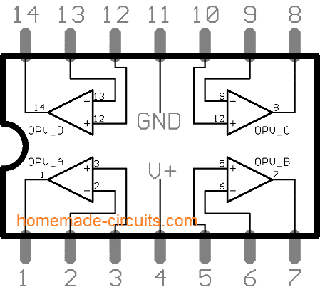
Next we'll take a look at the pin diagram of LM 324:

Pin Description:
There are 4 individual amplifiers / op-amps.
• Pin #1 is the output for first amplifier (left bottom)
• Pin #2 and #3 are the input for the first amplifier.
• Pin #4 is Vcc who’s maximum input voltage is 30V / +/-15V.
• Pin #5 and #6 are the input for second amplifier (right bottom)
• Pin #7 is the output for second amplifier.
• Pin #8 is output for third amplifier (right top)
• Pin #9 and #10 are two inputs for third amplifier.
• Pin #11 is ground.
• Pin #13 and #12 are inputs for fourth amplifier (top left)
• Pin #14 is the output for fourth amplifier.
• (+) represents non inverting input.
• (-) represents inverting input.
Absolute Maximum ratings and operating conditions:
Absolute maximum ratings are at-most limit of the component beyond which the component will not work as described / get damaged permanently.
Supply voltage: If your supply is dual supply (absolute) maximum is +/- 16V. If your power supply is single supply 32VDC.
Input differential voltage range: +/- 32 VDC: This range refers to the voltage difference that could be applied across the input pinouts of each of the opamps.
Input common mode voltage range: -0.3 to 32 VDC: These are the maximum and the minimum common mode input signal levels that may appear across the inputs of the opamp.
Junction temperature: 150 degree Celsius: It is the temperature that should not be exceeded at any cost on the IC, otherwise that mat cause a permanent damage to the IC
Power dissipation: 400 milliwatt: It is the amount of heat dissipation that the IC can withstand, and the limit at which its junction temperature could rise to 150 degree Celsius. Although this may be corrected with a heatsink, ICs should never be subjected to direct high power loads without appropriate buffer stages.
Storage temperature: -65 to +150 degree Celsius: Nothing critical here, as the range is well within any country's climatic conditions.
Operating ambient temperature: 0 to +70 degree Celsius: While operating the IC, the ambient or the surrounding temperature must be ideally below 70 degrees Celsius otherwise unpredictable things can occur with the IC performance.
Electrical characteristics (VCC+ = 5 V, VCC- = Ground, Vo = 1.4 V, Temp = 25 °C)
• Input offset voltage: typical: 2 mV, maximum: 7 mV.
• Input offset current typical: 2 nA, maximum: 20 nA.
• Input bias current typical: 20 nA, maximum: 100 nA.
• Large signal voltage gain ( Vcc = 15 v, RL, = 2 kohm, Vo = 1.4 V to 11.4 V): min: 50 V/mV, max: 100 V/mV.
• Slew rate (Vcc = 15 V, Vi = 0.5 V to 3 V, RL = 2 Kohm, CL = 100pF, unity gain) typical: 0.4 V/uS
• Output current source [Vid = 1 V] (Vcc = 15 V, Vo = 2V): minimum: 20 mA, Typical: 40 mA, Maximum: 70 mA.
• Output sink current [Vid = -1 V] (Vcc = 15 V, Vo = 2V) Minimum: 10mA, Typical: 20 mA.
• High Level Output Voltage (Vcc = 30 V, RL = 2 K ohm) Minimum: 26 V, Typical: 27 V.
• High Level Output Voltage (Vcc = 5 V, RL = 2 K ohm) Minimum: 3 V.
• Low Level Output Voltage (RL = 10 k Ohm) Typical: 5 mV, Maximum: 20mV.
• Total harmonic distortion (f = 1kHz, Av = 20 dB, RL = 2 kΩ, Vo = 2 Vpp, CL = 100 pF, VCC = 30 V) Typical: 0.015 %.
• Gain Bandwidth Product (VCC = 30 V, f = 100 kHz, Vin = 10 mV, RL = 2 kΩ, CL = 100 pF ) Typical : 1.3 MHz.
Application circuits:
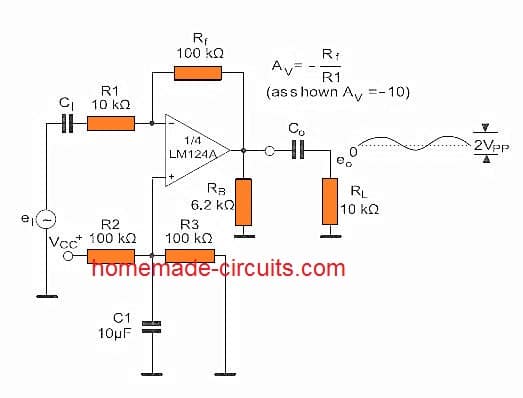
AC coupling Inverting Amplifier:

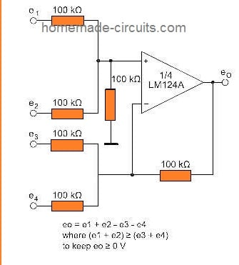
DC summing Amplifier:

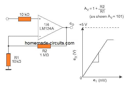
Non Inverting DC Gain:

Feel free to report any errors or questions via comment section you may get a quick reply.