You may have heard a lot about the outstanding features of the IC LM3524 or the SG3524, however many of you may not be confident regarding how to set up the pinout functioning of these ICs? Or you may be wondering exactly how to use the IC for your specific needs and application designs?
The paragraphs below explains everything you wanted to know regarding the working and practical implementation of the IC LM3524.

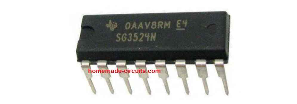
Main Features
Any seasoned electronic hobbyist will know the importance of this exceptionally versatile PWM controller IC LM3524, which is also popularly available with the prefix SG3524 and its series counterparts like SG3525 etc.
The IC LM3524 or the SG3524 both are pin to pin compatible, and feature a host of outstanding onboard features such as :
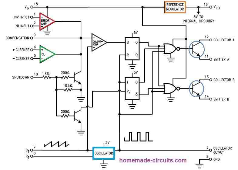
- Fixed 5V Reference Source
- Precision Totem pole output with guaranteed deadtime.
- Inbuilt oscillator with externally configurable RC timing parts.
- An integrated Error Amplifier for implementing an automatic output voltage correction
- An On-chip Current sense amplifier for implementing an automatic output current control feature
Main Applications
- Inverters and Converters
- Switching Power Supplies
- Motor Control
- Robotics
- Drones
- Buck Boost Regulators
- Solar Controllers
- Battery Charges
Absolute Maximum Ratings
The absolute maximum ratings refer to the maximum voltage and current parameters the IC LM3524 or the SG3524 are able to tolerate. The absolute maximum range informs us that the IC may burn or get permanently damaged if these parameter limits are exceeded

From the above table, the basic facts that we realize is that the LM3524 maximum operating must not be exceeded the 40 V limit.
The maximum current handling capacity of the output pins of the IC is around 200 mA, for LM3524 chip, and is 100 mA for the SG3524 device.
Reference Regulator
The LM3524D features a built-in 5V, 50 mA, short-circuit proof voltage regulator (indicated in orange square). This voltage regulator enables powering of all the internal circuitry of the chip and also works as a fixed external reference.
When the input supply voltage to the IC is below 8 V, the 5 V reference pin#15 VREF must be connected directly to pin#15, (VIN), in order to bypass the 5V regulator with the direct DC supply, as shown below. In this situation, the input voltage should not exceed 6V.

If the input supply is above 6V and 8V, then an external voltage regulator will become necessary, and can be easily implemented through an ordinary 7805 IC
Oscillator
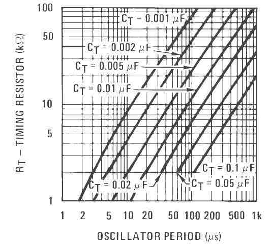
The LM3524D includes an on-board regulated oscillator stage. Its frequency is defined through an external resistor, RT and a complementing external capacitor, CT.
The formula for calculating the output frequency using RT and CT is given below:
fosc = 1 / RTCT
A graph plotted for RT, CT values with reference to their resulting oscillator frequency can be seen in Figure below.
As shown in the following diagram, the pulses from the oscillator's output is used for switching an internal flip-flop stage. This flip-flop then forwards the PWM data across the outputs of the IC, along with a blanking pulse which is used for shutting down the two outputs during the transition or crossover thresholds.
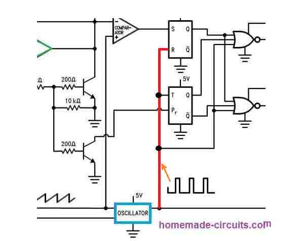
This completely prevents any risk of cross-conduction across the two outputs of the IC. The blanking pulse is also referred to as the "deadtime" whose width or the pulse OFF time is governed by the value of CT, as indicated in the following graph.
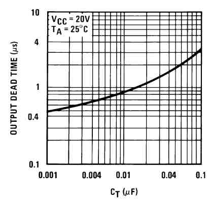
In the above CT vs deadtime graph we can see that as the capacitor CT value increases, the output "deadtime" also increases proportionately.
The value of RT is advised to be within 1.8 kΩ to 100 kΩ, while CT should be within the boundary of 0.001 μF to 0.1 μF, to ensure normal working of the IC.
Synchronization
For applications that require combining more than two LM3524D's to work in a synchronized manner, it is simply implemented by joining all the pin#3's, and joining all the pin#7's with each other to a single common CT capacitor, and keep all pin#6's unconnected, except the one that is associated with the solitary RT resistor. This procedure works nicely only as long as the ICs are not placed greater than 6″ apart.
An alternate synchronization technique may be possible, which can be applied without any restrictions on the IC placement. In this technique one of the LM3524D ICs, is wired up as the master chip, which must include the essential RT/CT timing elements, for setting up the intended correct oscillation frequency.
The other LM3524D(s) ICs can be then configured as slave units, and these must each include their individual RT/CT fixed with a 10% longer period than the master. After this, the pin#3's of all the ICs could be interconnected so that the master chip is able to reset all the slave units appropriately.
Synchronizing with an External Clock
In case it becomes necessary to synchronize the IC with an external clock source, this could be accomplished by setting up RT/CT in a way that the internal free-running oscillator frequency runs at 10% slower rate than the external clock.
Next, the pin#3 of the IC may be integrated with an approximately 3 V frequency derived from the external clock source. Pulse width must be higher than 50 ns to guarantee 100 % synchronization.
Error Amplifier
The IC LM3524 includes an error amplifier configured internally like a differential input, transconductance amplifier. Its gain is fixed at a minimal 86 dB either using a feedback or by incorporating an output loading. This output loading is possible either through a fully resistive load or through both a resistive and reactive elements.
The error amplifier works like a comparator when it pin#1 and pin#2 are appropriately configured with a feedback signal from the output of the IC. One of the input pins of the error amplifier is referenced to a fixed voltage level (such as 5 V), while the other pin is connected with the feedback loop from the IC output.
If this feedback signal tends to rise above the reference voltage level, the error amplifier output becomes active internally, such that it forces the flip-flop to narrow down the output PWM, and thus restore the output voltage and the feedback signal back to normal level
The error amplifier's inputs are rated with a common-mode input voltage range between 1.5V–5.5V. Meaning, the potential difference between the pin#2 and pin#1 must not be lower than 1.5 V, and higher than 5.5 V. The existing in-built regulator 5 V output could be used here as the reference, for biasing the op amp inputs for ensuring the specified range.
How to Connect Pin#9 Compensation
The output of the error op amp amplifier, which internally connects with the pulse width modulator input (pin#9), could be easily overridden with an external adjustable DC, due to its very high impedance i(ZO ≃ 5 MΩ).
This means that, an external adjustable DC voltage could be applied to pin#9 in order to overpower the error amplifier actions. The output pins are then forced to work with the PWM determined by the level of this external DC at pin#9.
The above implementation could be tested with a unregulated motor speed control in which an adjustable DC voltage is forced to pin#9 of the IC to regulate motor speed by varying this DC voltage.
The duty cycle is equivalent to the ratio proportion of each output's ON-time to the oscillator period. If the outputs are connected in parallel it will increase the witnessed duty cycle two fold.
How to Connect the Error Amplifier
In the above paragraph I have explained the functioning of the in-built error amplifier op amp of the IC LM3524D, now I have explained how this facilitates the automatic control of the output PWM with reference to an triggering source.
The following diagram explains the basic configuration:
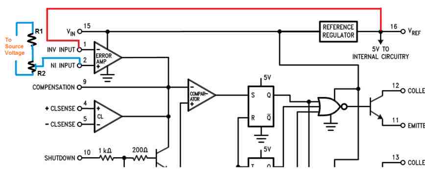
Here we can see that the pin#1 which is the inverting input of the op amp is connected with the IC's in-built +5V reference at pin#15.
Pin#2 of the error amp which is its non-inverting input is wired with a potential divider network using R1, R2, where R2 is a preset.
The ends of the R1/R2 are connected to the trigger source through the which output PWM needs to be regulated. For example, suppose we want to ensure a fixed output voltage from an LM3524D based inverter circuit, then the this trigger source input could be derived from the output of the inverter transformer, through a bridge network.
R2 preset is adjusted such that the potential at pin#2 is just a shade below the reference +5V at pin#1, when the output voltage is just below the highest unsafe threshold.
This means that, now if the the output voltage tends to rise above the unsafe voltage limit, would proportionately cause the DC at pin#2 to exceed the pin#1, 5V reference level. As soon as this happens, the error amplifier output would go high, causing the IC's output PWM to narrow down to a level which would force the output voltage to restore back to the specified safe lower limits.
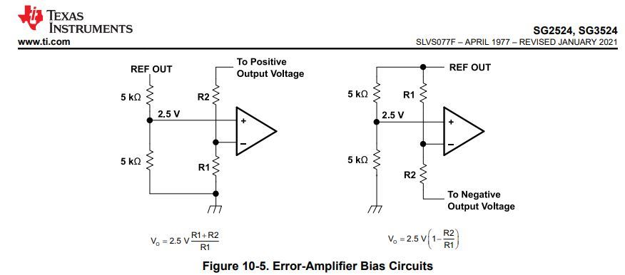
There are other methods also that can be employed for configuring the error amplifier op amp with external sources in order to control output over voltage parameter. The following diagrams were presented in the datasheet of SG3524.
Current Limiting
The purpose of the current limit amplifier is to overpower the error amplifier's output, so that it now controls the pulse width of the IC. When the CL op amp of the IC is used for the current limiting actions, a detection of an over-current will enable the op amp output to reduce the output PWM by as much as 25%. The over-current just needs to be translated into a 200 mV potential between the +CL and −CL sense terminals.
If this sense voltage increases by approximately 5% might force the output PWM to go down to as low as 0% duty cycle. However, one must make sure that the sensing potential across the +CL and −CL remains within the limits of −0.7V and +1.0V, input common-mode range.
How to Implement Current Control
The current limiting feature for the above implementation can be easily achieved through a sense resistor as shown below. The reliability of this current limiting feature depends on how accurate the sensing resistor is, and also by a tiny offset current, normally 100 μA, passing from +CL to −CL.
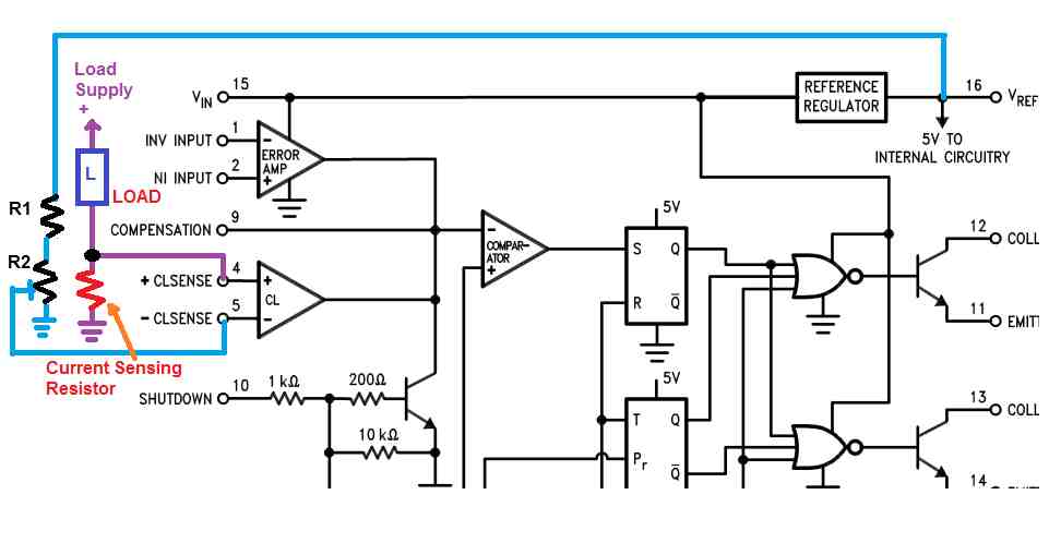
In the above figure we can see the standard way of configuring the current sense (CL) op amp of the LM3524D IC.
Here, too the reference voltage is acquired from the existing 5 V supply at pin#15 VREF of the IC.
This 5 V refernce is applied to the inverting input of the CL op amp through a resistive divider network.
The non-inverting input pin +CL is rigged between the load and a series connected current sensing resistor.
The preset R2 is adjusted such that the reference is dropped to a level that is just a few millivolts higher than the voltage drop expected to develop across the current sensing resistor, during an over load or over current conditions.
Normally, the preset is set such that the -CL pin gets around 0.4 V, which means, the voltage across the current sensing resistor must rise to around 0.6 V to trigger the op amp for the required PWM control of the output.
Therefore, the sensing resistor could be calculated as RS = 0.6 / Max Current Limit.
The current sensing can be also configured in the following simple manner, without depending on the 5 V reference input:
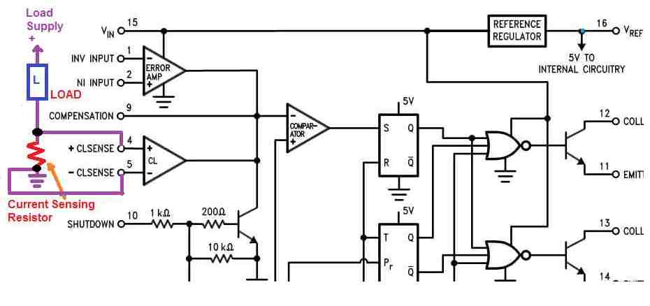
The sensing resistor must be calculated to ensure that the over current situation creates a voltage difference of not more than 0.5 V or 1 V, to keep the resistor value as small as possible.
Remember, the "LOAD" indicated in the above diagrams are supposed to be associated with the output of the IC.
Output Stages
The IC LM3524D outputs are internally configured with NPN transistors, with open collectors and emitters. The open collector/emitter allows the user with greater diversity and options to configure the output pins in many different ways, depending on individual specifications.
These outputs are designed to handle a maximum current of 200 mA. The internal transistors associated with the output pins are switched with a 180° out of phase current and voltage.
For Push-Pull Output Applications: For configure the output pins of the SG3524 IC, or the LM3524 IC, you can implement any one of the following designs, both will give identical response for driving the output power transistors in push-pull manner.
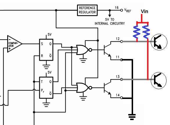
In the above configuration the IC's internal transistors are configured with the output power transistors as common base amplifier, which enables an alternate push-pull conduction of the output transistors and the load. This set up can be used in push-pull 12 V to 220 V PWM inverter applications.
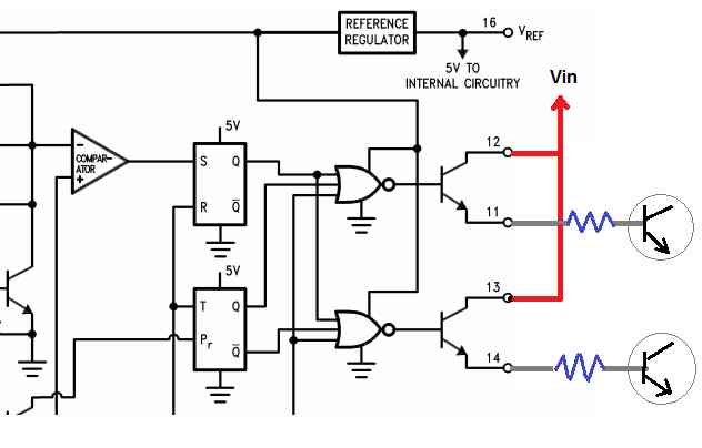
The second LM3524 output configuration will also deliver a push pull action on the output load and the transistors, however, here the IC's internal transistors as emitter-followers, which ultimately work like Darlington pairs wit the output power transistors enabling a high gain and current push pull conduction of the transistors and the load. Again, this set up also becomes for constructing power inverters.
For Single Ended Applications: For single ended output configurations, where the output power transistor and the load is supposed to work with simple ON/OFF switching, the following set ups could be employed:
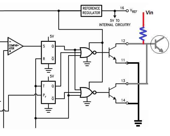
In the above set up the internal transistors can be seen joined in parallel and work as logic inverters for the load. When the internal transistors switch ON, the output transistors and the load switch OFF and vice versa.
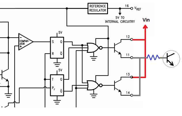
In the next single ended application set up above, the collectors of the internal ttarsistors are connected together with the positive and the emitters are connected together with the output transistor.
Here, the IC driver output transistors work as emitter followers with the output transistors and provide a high gain single ended operation for the load.
Wrapping Up
In the above posts I will comprehensively explained how the LM3524 and the SG3524 ICs work, their pinout functioning and the how to connect these ICs for practical applications.
We understood that these ICs are specifically designed as power regulators, and can be ideally implemented in power supply applications, with enhanced features such as automatic PWM control, automatic output over voltage correction, automatic over current control and constant current output.
We also learned how to use and set up the on-chip facilities of the IC such as PWM control, adjustable frequency, automatic dead time, error amplifier and the current sense amplifier.
If you have any further questions regarding the SG3524 or the LM3524 IC functions, or pinout details, or a specific application circuit, please feel free to express the same through your comment below:

Have Questions? Please Leave a Comment. I have answered over 50,000. Kindly ensure the comments are related to the above topic.
hello ….. i want to make a stable 50hz inverter with feedback using this 3524 ic ….. do you have the circuit diagram????
Hi, you can try the following design:
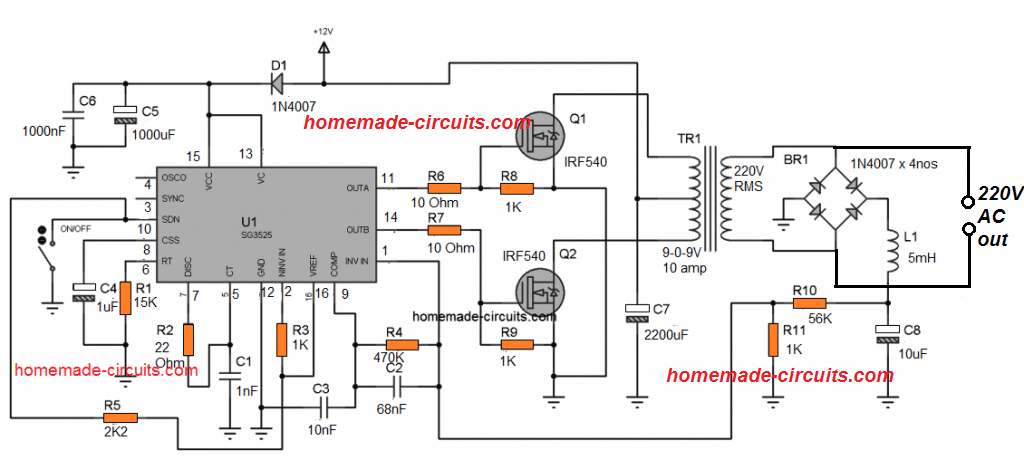
CT 1nf for which frequency please?
Sorry, I don’t remember it now, you may have to calculate it or check it practically.
How can MOSFETs to switch an inverter power transformer be wired into the above circuits as you have only shown external output transistors?
You can do it as shown in the 3rd circuit from this article:
https://www.homemade-circuits.com/sg3525-pure-sinewave-inverter-circuit/
Hi. very thorough explanation. Thank you.
For fun and education, I make up this circuit
https://www.arrow.com/it-it/reference-designs/typical-push-pull-transformer-coupled-circuit-for-sg3524-regulating-pulse-width-modulator/db400f9c01c4e80db994e844314bff74
with a 10 KOhm trimmer added along the feedback path but it doesn’t work.
Some measurements carried out
– VREF at PIN 16 (5V) -> OK
– Pulses on PIN3 -> OK
– Pulses on PIN3 are very narrow (Duty Cycle around 0,4%) whilst outputs (PIN11 and PIN14) are always at 50% DC.
– between PIN 1 and PIN2 (IN- and IN+ inputs of internal error amplifier) there is a voltage drop of about 1 V. Do you think is ok? I expected to read 0V.
Do you suspect a bad IC1?
Thank you
Hi, glad you liked the post. did you try adjusting the 5K resistor connected between pin#1 and ground, this might work to adjust the feedback.
Pin#16 generates the 5.1 V reference, and this potential is divided by the two 5K resistor at pin#2, so pin#2 must have a reference of 2.4V. If this reference is crossed by the pin#1 it must result in an output PWM correction. So normally pin1 potential must be lower than pin#2 potential, according to me
I don;t think your IC is bad otherwise you wouldn’t have got a 50% duty cycle frequency at the output pins
Thank you for the explanation.
If possible I would like french explanation because some phrases are not comprehensible in using google translation.
Question: have you a diagram that uses an optocoupler for the regulation?
Hi, Since I do not know french, so translating it to french will be difficult for me. I do not have an opto coupler based feedback circuit at this moment, will try to update it soon, if it is possible.
Using homemade circuits with the 3524 chip, I’ve had difficulty getting a reliable pulse output for operating another project which calls for 144 Khz. pulsing to operate. I need a circuit that’ll give this to me. Thanks for any help you can give. -Bill.
LM3524 output is normally extremely stable. Did you use the error amp feedback for correcting.
Also the input supply must be higher than 8 V
very good explanation !
Does it have a square wave output or sine wave ?
can this IC produce a sine wave output at 230 vac using power transistors and 9 /230 vac transformer?
Any application please ?
Thanks
bye
Thank you for liking the post!
The output will be square wave, not sinewave!
You can find a few good converter application designs in the following post:
https://www.ti.com/lit/ds/symlink/lm3524d.pdf