So far we have been studying BJT analysis dependent on the level of β over their corresponding operating points (Q-point). In this discussion we will check out how a given circuit conditions can help in determining the possible range of operating points or Q-points and in establishing the actual Q-point.
What is Load Line Analysis
In any electronic system the load applied on a semiconductor device will generally produce a significant impact on the point of operation or the region of operation of a device.
If an analysis is carried out through a graph drawing, we would be able to draw straight line across the characteristics of the device for establishing the applied load. The intersection of the load line with the characteristics of the device can be used for determining the point of operation or the Q-point of the device. This sort of an analysis is, for apparent reasons, known as load-line analysis.
How to Implement Load Line Analysis
The circuit shown in the following Fig 4.11(a) determines an output equation which provides a relationship between the variables IC and VCE as shown below:
VCE = VCC - ICRC (4.12)

Alternately, the output characteristics of the transistor as shown in the diagram (b) above also provide the relationship between the two variables IC and VCE.
This essentially helps us to get a circuit diagram based equation and a range of characteristics through a graphical representation which work with similar variables.
The common outcome from the two is established when the constraints defined by them are fulfilled simultaneously.
Alternatively this may be understood as solutions being achieved from two concurrent equations, where one is set up with the help of the circuit diagram, while the other from the BJT datasheet characteristics.
In Fig. 4.11b we can see the characteristics IC vs VCE of the BJT, so now we are able to superimpose a straight line described by the Eq (4.12) over the characteristics.
The easiest method of tracing Eq (4.12) over the characteristics could be executed by the rule which says that any straight line is determined by two distinct points.
By selecting IC = 0mA, we find the horizontal axis becomes the line where one of the points takes its position.
Also by replacing IC = 0mA in Eq (4.12) we get:

This determines one of the points for the straight line, as indicated in fig 4.12 below:

Now if we choose VCE = 0V, this sets up the vertical axis as the line where our second point takes its position. With this situation, now we are able to find that IC can be evaluated by the following equation.

which can be clearly witnessed on Fig. 4.12.
By connecting the two points as determined by Eqs. (4.13) and (4.14), a straight line as established by Eq 4.12 could be drawn.
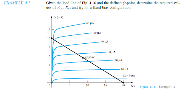
This line as seen on the graph Fig 4.12 is recognized as the load line since it is characterized by the load resistor RC.
By solving the established level of IB, the actual Q-point could be fixed as shown in Fig 4.12
If we vary the magnitude of IB by varying the RB value, we find the Q-point shifts towards upward or downward across the load line as depicted in Fig. 4.13.

If we maintain a constant VCC, and change only the value of RC, we find the load line shifting as indicated in Fig 4.14.
If we keep IB constant, we find the Q-point changing its position as indicated in the same figure 4.14.And if we keep RC constant, and vary only VCC, we see load line moving as depicted in Fig 4.15

Solving a Practical Load Line Analysis Example


Reference: https://en.wikipedia.org/wiki/Load_line_(electronics)