In this post I will comprehensively explain what logic gates are and its working. We will be taking a look at the basic definition, symbol, truth table, Multi input gates, we will be also constructing transistor based gate equivalents and finally we will take an overview on various relevant CMOS ICs.
What are Logic Gates
A logic gate in an electronic circuit can be expressed as a physical unit represented through a Boolean function.
In other words, a logic gate is designed to execute a logical function using single or more binary inputs and to generate a single binary output.
Electronic Logic gates are fundamentally configured and implemented using semiconductor blocks or elements such as diodes or transistors which work like ON/OFF switches having a well-defined switching pattern. Logic gates facilitate cascading of the gates such that it easily enables composition of Boolean functions, making it possible to create physical models of all Boolean logic. This further enables algorithms and mathematics writable using Boolean logic.
Logic circuits may employ semiconductor elements in the range of multiplexers, registers, arithmetic logic units (ALUs), and computer memory, and even microprocessors, involving as high as 100s of millions of logic gates. In today’s implementation, you will find mostly field-effect transistors (FETs), being used for manufacturing logic gates, a good example being a metal–oxide–semiconductor field-effect transistors or MOSFETs.
Let's begin the tutorial with logic AND gates.
What is Logic “AND” Gate?
It is an electronic gate, whose output turns “high” or “1” or “true” or gives out a “positive signal” when all the inputs of the AND gates are “high” or “1” or “true” or “positive signal”.
For example: Say in an AND gate with ‘n’ number of inputs, if all the inputs are “high” the output turns “high”. Even if one input is “LOW” or “0” or “false” or “negative signal”, the output turns “LOW” or “0” or “false” or gives out a “negative signal”.
Note:
The term “High”, “1”, “positive signal”, “true” are essentially the same (Positive signal is the battery’s or power supply’s positive signal).
The term “LOW”, “0”, “negative signal”, “false” are essentially the same (Negative signal is the battery’s or power supply’s negative signal).
Illustration of Logic AND gate symbol:

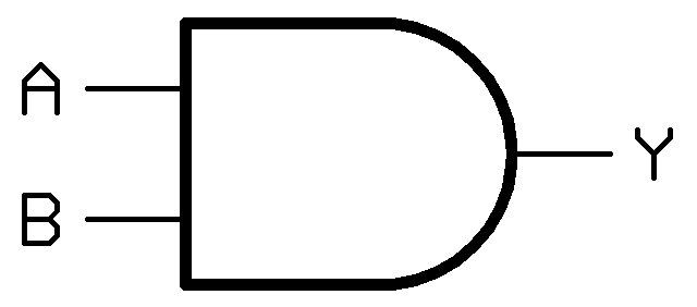
Here the “A” and “B” are the two inputs and the “Y” is output.
The Boolean expression for logic AND gate: The output ‘Y’ is multiplication of the two inputs ‘A’ and ‘B’. (A.B) = Y.
The Boolean multiplication is denoted by a dot (.)
If ‘A’ is ‘1’ and ‘B’ is ‘1’ the output is (A.B) = 1 x 1 = ‘1’ or “high”
If ‘A’ is ‘0’ and ‘B’ is ‘1’ the output is (A.B) = 0 x 1 = ‘0’ or “Low”
If ‘A’ is ‘1’ and ‘B’ is ‘0’ the output is (A.B) = 1 x 0 = ‘0’ or “Low”
If ‘A’ is ‘0’ and ‘B’ is ‘0’ the output is (A.B) = 0 x 0 = ‘0’ or “Low”
The above conditions are simplified in the truth table.
Truth Table (Two Input):
A (Input) | B (INPUT) | Y (Output) |
0 | 0 | 0 |
0 | 1 | 0 |
1 | 0 | 0 |
1 | 1 | 1 |
3-Input “AND” Gate:
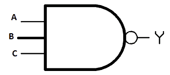
Illustration of 3 input AND gate:
Logic AND gates can have ‘n’ number of inputs, which means it can have more than two inputs (Logic AND gates will have at-least two input and always one output).
For a 3 input AND gate the Boolean equation turns like this: (A.B.C) = Y, similarly for 4 input and above.
Truth Table for 3 input logic AND gate:
A (INPUT) | B (INPUT) | C (INPUT) | Y (OUTPUT) |
0 | 0 | 0 | 0 |
0 | 0 | 1 | 0 |
0 | 1 | 0 | 0 |
0 | 1 | 1 | 0 |
1 | 0 | 0 | 0 |
1 | 0 | 1 | 0 |
1 | 1 | 0 | 0 |
1 | 1 | 1 | 1 |
Multi Input Logic AND Gates:
Commercially available Logic AND gates are only available in 2, 3 and 4 inputs. If we have more than 4 input then we have to cascade the gates.
We can have six input logic AND gates by cascading the 2 input AND gates as follows:
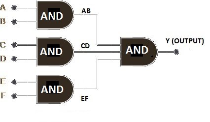
Now the Boolean equation for the above circuit becomes Y = (A.B).(C.D).(E.F)
Still, all the mentioned logical rules apply to the above circuit.
If you are going to use only 5 inputs from the above 6 inputs AND gates, we can connect a pull-up resistor at any one pin and now it becomes 5 input AND gate.
Transistor Based two input Logic AND gate:
Now we know, how a logic AND gate functions, let’s construct a 2 input AND gate using two NPN transistors. The logic ICs are constructed in the almost same the same way.
Two Transistor AND gate Schematic:
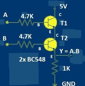
At the output “Y” you can connect a LED; if the output is high the LED will glow (LED +Ve terminal at “Y” with 330 ohm resistor and negative to GND).
When we apply high signal to the base of the two transistors, both the transistors turns ON, the +5V signal will be available at the emitter of the T2, thus the output turns high.
If any one of the transistor is OFF, no positive voltage will be available at emitter of T2, but due to the 1K pull down resistor the negative voltage will be available at the output, so the output is referred as low.
Now you know how to construct logic AND gate of your own.
Quad AND gate IC 7408:
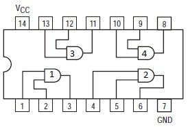
If you want to buy logic AND gate from the market, you will get in the above configuration.
It has 14 pins; the pin #7 and pin #14 are GND and Vcc respectively. It is operated at 5V.
Propagation delay:
Propagation delay is the time taken for the output to change from LOW to HIGH and vice versa.
The propagation delay from LOW to HIGH is 27 nanoseconds.
The propagation delay from HIGH to LOW is 19 nanoseconds.
Other commonly available “AND” gate ICs:
• 74LS08 Quad 2-input
• 74LS11 Triple 3-input
• 74LS21 Dual 4-input
• CD4081 Quad 2-input
• CD4073 Triple 3-input
• CD4082 Dual 4-input
You can always refer data sheet for the above ICs for more information.
How Logic “Exclusive NOR” Gate Function
In this post I am going to explain about logic “Ex-NOR” gate or Exclusive-NOR gate. We will be taking a look at the basic definition, symbol, truth table, Ex-NOR equivalent circuit, Ex-NOR realization using logic NAND gates and finally, we will be taking overview on quad 2 input Ex-OR gate IC 74266.
What is “Exclusive NOR” gate?
It is an electronic gate, whose output turns “high” or “1” or “true” or gives out a “positive signal” when the inputs are even number of logic “1s” (or “true” or “high” or “positive signal”).
For example: Say an Exclusive NOR gate with ‘n’ number of inputs, if the inputs are logic “HIGH” with 2 or 4 or 6 inputs (even number of input “1s”) the output turns “HIGH”.
Even if we apply no logic “high” to input pins (i.e. zero number of logic “HIGH” and all logic “LOW”), still “zero” is an even number the output turns “HIGH”.
If the number of logic “1s” applied are ODD then the output turns “LOW” (or “0” or “false” or “negative signal”).
This is opposite of logic “Exclusive OR” gate where its output turns “HIGH” when the inputs are ODD number of logic “1s”.
Note:
The term “High”, “1”, “positive signal”, “true” are essentially the same (Positive signal is the battery’s or power supply’s positive signal).
The term “LOW”, “0”, “negative signal”, “false” are essentially the same (Negative signal is the battery’s or power supply’s negative signal).
Illustration of Logic “Exclusive NOR” gate:
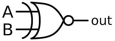
“Exclusive NOR” gate equivalent Circuit:

The above is the equivalent circuit for logic Ex-NOR, which is basically combination of logic “Exclusive OR” gate and logic “NOT” gate.
Here the “A” and “B” are the two inputs and the “Y” is output.
The Boolean expression for logic Ex-NOR gate: Y = (AB) ̅ + AB.
If ‘A’ is ‘1’ and ‘B’ is ‘1’ the output is ((AB) ̅ + AB) = 0 + 1 = ‘1’ or “HIGH”
If ‘A’ is ‘0’ and ‘B’ is ‘1’ the output is ((AB) ̅ + AB) = 0 + 0 = ‘0’ or “LOW”
If ‘A’ is ‘1’ and ‘B’ is ‘0’ the output is ((AB) ̅ + AB) = 0 + 0 = ‘0’ or “LOW”
If ‘A’ is ‘0’ and ‘B’ is ‘0’ the output is ((AB) ̅ + AB) = 1 + 1 = ‘1’ or “HIGH”
The above conditions are simplified in the truth table.
Truth Table (Two Input):
A (Input) | B (INPUT) | Y (Output) |
0 | 0 | 1 |
0 | 1 | 0 |
1 | 0 | 0 |
1 | 1 | 1 |
3 Input Exclusive NOR Gate:
Illustration of 3 input Ex-NOR gate:
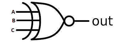
Truth Table for 3 input logic EX-OR gate:
A (INPUT) | B (INPUT) | C (INPUT) | Y (OUTPUT) |
0 | 0 | 0 | 1 |
0 | 0 | 1 | 0 |
0 | 1 | 0 | 0 |
0 | 1 | 1 | 1 |
1 | 0 | 0 | 0 |
1 | 0 | 1 | 1 |
1 | 1 | 0 | 1 |
1 | 1 | 1 | 0 |
For the 3 input Ex-NOR gate the Boolean equation becomes: A ̅(BC) ̅ + ABC ̅ + AB ̅C + A ̅BC.
The logic “Ex-NOR” gate is not a fundamental logic gate but, combination of different logic gates. The Ex-NOR gate can be realized using logic “OR” gates, logic “AND” gate and logic “NAND” gate as follows:
Equivalent circuit for “Exclusive NOR” gate:
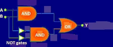
The above design has major drawback, we need 3 different logic gates to make one Ex-NOR gate. But we can overcome this problem by implementing Ex-NOR gate with only logic “NAND” gates, this is also economical to fabricate.
Exclusive NOR gate using NAND gate:
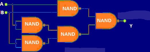
Exclusive NOR gates are used to perform complicated computing tasks such as arithmetic operations, binary adders, binary subtraction, parity checkers and they are used as digital comparators.
Logic Exclusive-NOR Gate IC 74266:
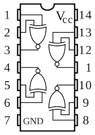
If you want to buy logic Ex-NOR gate from the market, you will get in the above DIP configuration.
It has 14 pins; the pin #7 and pin #14 are GND and Vcc respectively. It is operated at 5V.
Propagation delay:
Propagation delay is the time taken for the output to change from LOW to HIGH and vice versa after giving input.
The propagation delay from LOW to HIGH is 23 nanoseconds.
The propagation delay from HIGH to LOW is 23 nanoseconds.
Commonly available “EX-NOR” gate ICs:
74LS266 Quad 2-input
CD4077 Quad 2-input
How NAND Gate Works
In the below explanation we are going to explore about digital logic NAND gate. We will be taking a look at the basic definition, symbol, truth table, Multi input NAND gate, we will be constructing transistor based 2 input NAND gate, various logic gates using only NAND gate and finally we will take an overview on the NAND gate IC 7400.
What is Logic “NAND” Gate?
It is an electronic gate, whose output turns “LOW” or “0” or “false” or gives out a “negative signal” when all the inputs of the NAND gates are “high” or “1” or “true” or “positive signal”.
For example: Say an NAND gate with ‘n’ number of inputs, if all the inputs are “high” the output turns “LOW”. Even if one input is “LOW” or “0” or “false” or “negative signal”, the output turns “HIGH” or “1” or “true” or gives out a “positive signal”.
Note:
The term “High”, “1”, “positive signal”, “true” are essentially the same (Positive signal is the battery’s or power supply’s positive signal).
The term “LOW”, “0”, “negative signal”, “false” are essentially the same (Negative signal is the battery’s or power supply’s negative signal).
Illustration of Logic NAND gate symbol:
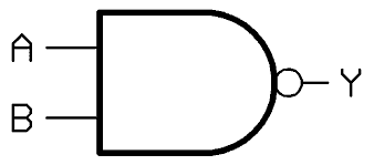
Here the “A” and “B” are the two inputs and the “Y” is output.
This symbol is “AND” gate with inversion “o”.
Logic “NAND” Gate Equivalent Circuit:

The logic NAND gate is the combination of logic “AND” gate and logic “NOT” gate.
The Boolean expression for logic NAND gate: The output ‘Y’ is complementary multiplication of the two inputs ‘A’ and ‘B’. Y = ((A.B) ̅)
The Boolean multiplication is denoted by a dot (.) and the complementary (inversion) is represented by a bar (-) over a letter.
If ‘A’ is ‘1’ and ‘B’ is ‘1’ the output is ((A.B) ̅) = (1 x 1) ̅ = ‘0’ or “LOW”
If ‘A’ is ‘0’ and ‘B’ is ‘1’ the output is ((A.B) ̅) = (0 x 1) ̅ = ‘1’ or “HIGH”
If ‘A’ is ‘1’ and ‘B’ is ‘0’ the output is ((A.B) ̅) = (1 x 0) ̅ = ‘1’ or “HIGH”
If ‘A’ is ‘0’ and ‘B’ is ‘0’ the output is ((A.B) ̅) = (0 x 0) ̅ = ‘1’ or “HIGH”
The above conditions are simplified in the truth table.
Truth Table (Two Input):
A (Input) | B (INPUT) | Y (Output) |
0 | 0 | 1 |
0 | 1 | 1 |
1 | 0 | 1 |
1 | 1 | 0 |
3-Input “NAND” Gate:

Illustration of 3 input NAND gate:
Logic NAND gates can have ‘n’ number of inputs, which means it can have more than two inputs
(Logic NAND gates will have at-least two input and always one output).
For a 3 input NAND gate the Boolean equation turns like this: ((A.B.C) ̅) = Y, similarly for 4 input and above.
Truth Table for 3 input logic NAND gate:
A (INPUT) | B (INPUT) | C (INPUT) | Y (OUTPUT) |
0 | 0 | 0 | 1 |
0 | 0 | 1 | 1 |
0 | 1 | 0 | 1 |
0 | 1 | 1 | 1 |
1 | 0 | 0 | 1 |
1 | 0 | 1 | 1 |
1 | 1 | 0 | 1 |
1 | 1 | 1 | 0 |
Multi Input Logic NAND Gates:
Commercially available Logic NAND gates are only available in 2, 3 and 4 inputs. If we have more than 4 input then we have to cascade the gates.
For example, we can have four input logic NAND gate by cascading 5 two input NAND gates as follows:

Now the Boolean equation for the above circuit becomes Y = ((A.B.C.D) ̅)
Still, all the mentioned logical rules apply to the above circuit.
If you are going to use only 3 inputs from the above 4 inputs NAND gate, we can connect a pull-up resistor to any one pin and now it becomes 3 input NAND gate.
Transistor Based two input Logic NAND gate:
Now we know, how a logic NAND gate functions, let’s construct a 2 input NAND gate using two
NPN transistors. The logic ICs are constructed in the almost same the same way.
Two Transistor NAND gate Schematic:
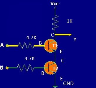
At the output “Y” you can connect a LED; if the output is high, the LED will glow (LED +Ve terminal at “Y” with 330 ohm resistor and negative to GND).
When we apply high signal to the base of the two transistors, both the transistors turns ON, the ground signal will be available at the collector of the T1, thus the output turns “LOW”.
If any one of the transistor is OFF i.e. applying “LOW” signal to base, no ground signal will be available at collector of T1, but due to the 1K pull up resistor the positive signal will be available at the output and the output is turns “HIGH”.
Now you know how to construct logic NAND gate of your own.
Various Logic Gates Using NAND gate:
The NAND gate is also known as “universal logic gate” because we can make any Boolean logic with this single gate. This is an advantage for fabricating ICs with different logical functions and fabricating a single gate is economical.
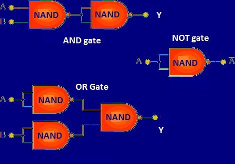
In above schematics just 3 types of gates are shown but, we can make any Boolean logic.
Quad NAND gate IC 7400:
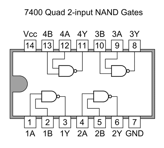
If you want to buy a logic NAND gate from the market, you will get in the above DIP configuration.
It has 14 pins; the pin #7 and pin #14 are GND and Vcc respectively. It is operated at 5V.
Propagation delay:
Propagation delay is the time taken for the output to change from LOW to HIGH and vice versa after giving an input.
The propagation delay from LOW to HIGH is 22 nanoseconds.
The propagation delay from HIGH to LOW is 15 nanoseconds.
There several other NAND gate ICs available:
- 74LS00 Quad 2-input
- 74LS10 Triple 3-input
- 74LS20 Dual 4-input
- 74LS30 Single 8-input
- CD4011 Quad 2-input
- CD4023 Triple 3-input
- CD4012 Dual 4-input
How NOR Gate Works
Here we are going to explore about digital logic NOR gate. We will be taking a look at the basic definition, symbol, truth table, Multi input NOR gate, we will be constructing transistor based 2 input NOR gate, various logic gates using only NOR gate and finally we will take an overview on the NOR gate IC 7402.
What is Logic “NOR” Gate?
It is an electronic gate, whose output turns “HIGH” or “1” or “true” or gives out a “positive signal” when all the inputs of the NOR gates are “LOW” or “0” or “false” or “negative signal”.
For example: Say an NOR gate with ‘n’ number of inputs, if all the inputs are “LOW” the output turns “HIGH”. Even if one input is “HIGH” or “1” or “true” or “positive signal”, the output turns “LOW” or “0” or “false” or gives out a “negative signal”.
Note:
The term “High”, “1”, “positive signal”, “true” are essentially the same (Positive signal is the battery’s or power supply’s positive signal).
The term “LOW”, “0”, “negative signal”, “false” are essentially the same (Negative signal is the battery’s or power supply’s negative signal).
Illustration of Logic NOR gate symbol:
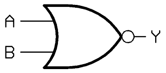
Here the “A” and “B” are the two inputs and the “Y” is output.
This symbol is “OR” gate with inversion “o”.
Logic “NOR” Gate Equivalent Circuit:

The logic NOR gate is the combination of logic “OR” gate and logic “NOT” gate.
The Boolean expression for logic NOR gate: The output ‘Y’ is complementary addition of the two inputs ‘A’ and ‘B’. Y = ((A+B) ̅)
The Boolean addition is denoted by (+) and the complementary (inversion) is represented by a bar (-) over a letter.
If ‘A’ is ‘1’ and ‘B’ is ‘1’ the output is ((A+B) ̅) = (1+ 1) ̅ = ‘0’ or “LOW”
If ‘A’ is ‘0’ and ‘B’ is ‘1’ the output is ((A+B) ̅) = (0+ 1) ̅ = ‘0’ or “LOW”
If ‘A’ is ‘1’ and ‘B’ is ‘0’ the output is ((A+B) ̅) = (1+ 0) ̅ = ‘0’ or “LOW”
If ‘A’ is ‘0’ and ‘B’ is ‘0’ the output is ((A+B) ̅) = (0+ 0) ̅ = ‘1’ or “HIGH”
The above conditions are simplified in the truth table.
Truth Table (Two Input):
A (Input) | B (INPUT) | Y (Output) |
0 | 0 | 1 |
0 | 1 | 0 |
1 | 0 | 0 |
1 | 1 | 0 |
3-Input “NOR” Gate:
Illustration of 3 input NOR gate:
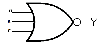
Logic NOR gates can have ‘n’ number of inputs, which means it can have more than two inputs (Logic NOR gates will have at-least two input and always one output).
For a 3 input NOR gate the Boolean equation turns like this: ((A+B+C) ̅) = Y, similarly for 4 input and above.
Truth Table for 3 input logic NOR gate:
A (INPUT) | B (INPUT) | C (INPUT) | Y (OUTPUT) |
0 | 0 | 0 | 1 |
0 | 0 | 1 | 0 |
0 | 1 | 0 | 0 |
0 | 1 | 1 | 0 |
1 | 0 | 0 | 0 |
1 | 0 | 1 | 0 |
1 | 1 | 0 | 0 |
1 | 1 | 1 | 0 |
Multi Input Logic NOR Gates:
Commercially available Logic NOR gates are only available in 2, 3 and 4 inputs. If we have more than 4 input then we have to cascade the gates.
For example, we can have four input logic NOR gate by cascading 5 two input NOR gates as follows:

Now the Boolean equation for the above circuit becomes Y = ((A+B+C+D) ̅)
Still, all the mentioned logical rules apply to the above circuit.
If you are going to use only 3 inputs from the above 4 inputs NOR gate, we can connect a pull-down resistor to any one of the pin and now it becomes 3 input NOR gate.
Transistor Based two input Logic NOR gate:
Now we know, how a logic NOR gate functions, let’s construct a 2 input NOR gate using two NPN transistors. The logic ICs are constructed in the almost same the same way.
Two Transistor NOR gate Schematic:
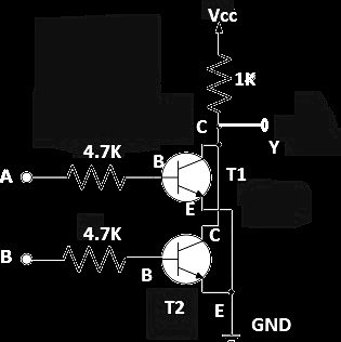
At the output “Y” you can connect a LED; if the output is high, the LED will glow (LED +Ve terminal at “Y” with 330 ohm resistor and negative to GND).
When we apply “HIGH” signal to the base of the two transistors, both the transistors turns ON and the ground signal will be available at the collector of the T1 and T2, thus the output turns “LOW”.
If we apply “HIGH” to any one of the transistor, still the negative signal will be available at the output, making the output go “LOW”.
If we apply “LOW” signal to the base of two transistors, both turns OFF, but due to the pull-up resistor the output turns “HIGH”.
Now you know how to construct logic NOR gate of your own.
Various Logic Gates Using NOR gate:
NOTE: NAND and NOR are the two gates otherwise known as universal gates.
The NOR gate is also a “universal logic gate” because we can make any Boolean logics with this single gate. This is an advantage for fabricating ICs with different logical functions and fabricating a single gate is economical, this is same for NAND gate too.
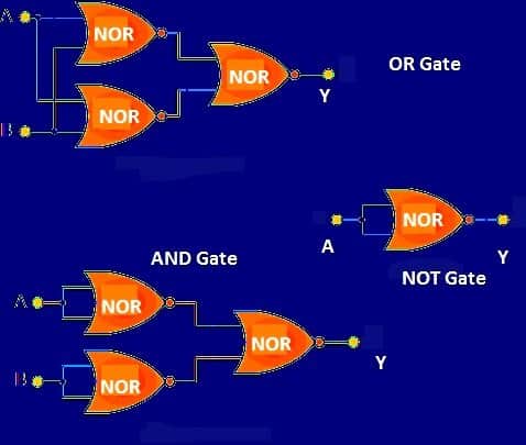
In above schematics just 3 types of gates are showcased but, we can make any Boolean logics.
Quad NOR gate IC 7402:
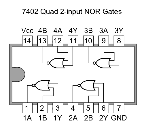
If you want to buy a logic NOR gate from the market, you will get in the above DIP configuration.
It has 14 pins; the pin #7 and pin #14 are GND and Vcc respectively. It is operated at 5V.
Propagation delay:
Propagation delay is the time taken for the output to change from LOW to HIGH and vice versa after giving an input.
The propagation delay from LOW to HIGH is 22 nanoseconds.
The propagation delay from HIGH to LOW is 15 nanoseconds.
There several other NOR gate ICs available:
- 74LS02 Quad 2-input
- 74LS27 Triple 3-input
- 74LS260 Dual 4-input
- CD4001 Quad 2-input
- CD4025 Triple 3-input
- CD4002 Dual 4-input
Logic NOT Gate
In this post I am going to explain about logic “NOT” gate. We will be learning about its basic definition, symbol, truth table, NAND and NOR gate equivalents, Schmitt inverters, Schmitt NOT gate oscillator, NOT gate using transistor and finally we will be taking a look at logic NOT gate inverter IC 7404.
Before we start looking into the detail of logic NOT gate which is also called as digital inverter, one must not confuse with the “Power inverters” that are used in solar or backup power supplies at home or office.
What is Logic “NOT” Gate?
It is a single input and single output logic gate whose output is complement to the input.
The above definition states that if the input is “HIGH” or “1” or “true” or “positive signal” the output will be “LOW” or “0” or “false” or “negative signal”.
If the input is “LOW” or “0” or “false” or “negative signal” the output will be inverted to “HIGH” or “1” or “true” or “positive signal”
Note:
The term “High”, “1”, “positive signal”, “true” are essentially the same (Positive signal is the battery’s or power supply’s positive signal).
The term “LOW”, “0”, “negative signal”, “false” are essentially the same (Negative signal is the battery’s or power supply’s negative signal).
Illustration of Logic NOT Gate:
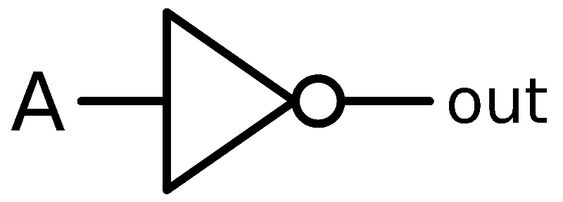
Let’s assume “A” is the input and “Y” is the output, the Boolean equation for logic NOT gate is: Ā = Y.
The equation states that the output is inversion of the input.
Truth Table for logic NOT gate:
A (INPUT) | Y (OUTPUT) |
0 | 1 |
1 | 0 |
The not gates will always have a single input (and always have a single output) it is categorized as decision making devices. The “o” symbol at the tip of the triangle represents complementation or inversion.
This “o” symbol is not only limited to the logic “NOT” gate, but also can be used by any logic gates or any digital circuit. If the “o” is at the input, this states that the input is active-low.
Active-Low: The output turns active (activating a transistor, a LED or a relay etc.) when “LOW” input is given.
NAND and NOR Gates Equivalent:

The “NOT” gate can be constructed using logic “NAND” and logic “NOR” gates by joining all the input pins, this applies to gates with 3, 4 and higher input pins.
Transistor based Logic “NOT” gate:
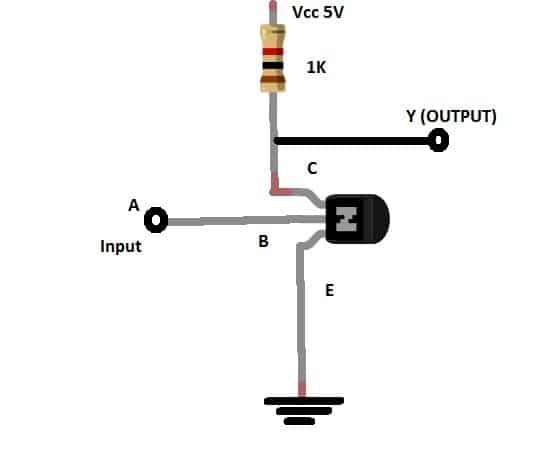
The logic “NOT” can be constructed by a NPN transistor and a 1K resistor. If we apply “HIGH” signal to the base of the transistor, the ground gets connected to the collector of the transistor, thus the output turns “LOW”.
If we apply “LOW” signal to the base of the transistor, the transistor remains OFF and will not connected to ground but, the output will be pulled “HIGH” by the pull-up resistor connect to Vcc. Thus we get can make a logic “NOT” gate using transistor.
Schmitt Inverters:
We will explore this concept with an automatic battery charger to explain the utilization and functioning of the Schmitt inverters. Let’s take the example of li-ion battery charging procedure.
The 3.7 V li-ion battery is charged when the battery hits 3 V to 3.2 V; the battery voltage rises gradually while charging and the battery needs to be cut-off at 4.2 V. After charging, the battery’s open circuit voltage drops around 4.0 V.
A voltage sensor measures the cut-off limit and triggers the relay to stop charging. But when the voltage drops below 4.2V the charger detects as not charged and begins the charge till 4.2V and cut-off, again the battery voltage falls to 4.0V and begins the charge again and this madness cycles over and over.
This will kill the battery quickly, to overcome this issue we need a lower threshold level or “LTV” so that the battery won’t start charge until the battery falls to 3 V to 3.2 V. The upper threshold voltage or “UTV” is 4.2V in this example.
A Schmitt inverter is made to switch its output state when the voltage crosses the upper threshold voltage and it stays same until the input reaches the lower threshold voltage.
Similarly, once the input is crosses lower threshold voltage, the output stays same until the input reaches the upper threshold voltage.
It won’t change its state in between the LTV and UTV.
Now, because of this, the ON / OFF will be much smoother and unwanted oscillation will be removed and also the circuit will more resistant to electrical noise.
Schmitt NOT Gate Oscillator:
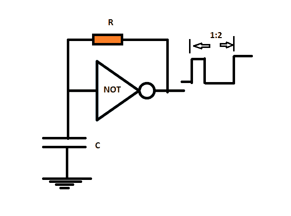
The above circuit is an oscillator which produce square wave at 33% duty cycle. Initially the capacitor is in discharged state and the ground signal will be available at input of NOT gate.
The output turns positive and charges the capacitor via resistor “R”, the capacitor charges till the upper threshold voltage of the inverter and changes the state, the output turns negative signal and capacitor starts to discharge via the resistor “R” until capacitor voltage reaches the lower threshold level and changes the state, the output turns positive and charges the capacitor.
This cycle repeats as long the power supply is given to the circuit.
The frequency of the above oscillator can be calculated: F= 680/RC
Where, F is frequency.
R is resistance in ohms.
C is capacitance in farad.
Square wave converter:
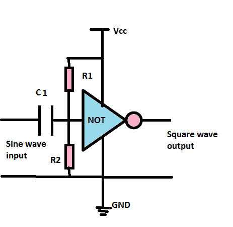
The above circuit will convert sine wave signal to square wave, actually it can convert any analog waves into square wave.
The two resistors R1 and R2 work as voltage divider, this is utilized to get a biasing point and the capacitor blocks any DC signals.
If the input signal goes above Upper threshold level or below lower threshold level the output turns
LOW or HIGH according to the signal, this produces square wave.
IC 7404 NOT gate Inverter:
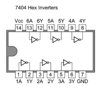
The IC 7404 is one of the most commonly used logic NOT gate IC. It has 14 pins, pin #7 is ground and pin #14 is Vcc. The operating voltage is from 4.5V to 5V.
Propagation delay:
The propagation delay is the time taken by the gate to process the output after giving an input.
In logic “NOT” gate takes around 22 nano seconds to change its state from HIGH to LOW and vice versa.
There are several other logic “NOT gate ICs:
• 74LS04 Hex Inverting NOT Gate
• 74LS14 Hex Schmitt Inverting NOT Gate
• 74LS1004 Hex Inverting Drivers
• CD4009 Hex Inverting NOT Gate
• CD4069 Hex Inverting NOT Gate
How OR gate Works
Now let's explore about digital logic OR gates. We will be taking a look at the basic definition, symbol, truth table, Multi input OR gate, we will be constructing transistor based 2 input OR gate and finally we will take an overview on the OR gate IC 7432.
What is Logic “OR” Gate?
It is an electronic gate, whose output turns “LOW” or “0” or “false” or gives out a “negative signal” when all the inputs of the OR gates are “LOW” or “0” or “false” or “negative signal”.
For example: Say an OR gate with ‘n’ number of inputs, if all the inputs are “LOW” the output turns “LOW”. Even if one input is “HIGH” or “1” or “true” or “positive signal”, the output turns “HIGH” or “1” or “true” or gives out a “positive signal”.
Note:
The term “High”, “1”, “positive signal”, “true” are essentially the same (Positive signal is the battery’s or power supply’s positive signal).
The term “LOW”, “0”, “negative signal”, “false” are essentially the same (Negative signal is the battery’s or power supply’s negative signal).
Illustration of Logic OR gate symbol:
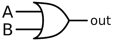
Here the “A” and “B” are the two inputs and the “Y” is output.
The Boolean expression for logic OR gate: The output ‘Y’ is addition of the two inputs ‘A’ and ‘B’, (A+B) = Y.
The Boolean addition is denoted by (+)
If ‘A’ is ‘1’ and ‘B’ is ‘1’ the output is (A + B) = 1 + 1 = ‘1’ or “high”
If ‘A’ is ‘0’ and ‘B’ is ‘1’ the output is (A + B) = 0 + 1 = ‘1’ or “high”
If ‘A’ is ‘1’ and ‘B’ is ‘0’ the output is (A + B) = 1 + 0 = ‘1’ or “high”
If ‘A’ is ‘0’ and ‘B’ is ‘0’ the output is (A + B) = 0 + 0 = ‘0’ or “Low”
The above conditions are simplified in the truth table.
Truth Table (Two Input):
A (Input) | B (INPUT) | Y (Output) |
0 | 0 | 0 |
0 | 1 | 1 |
1 | 0 | 1 |
1 | 1 | 1 |
3-Input “OR” Gate:
Illustration of 3 input OR gate:
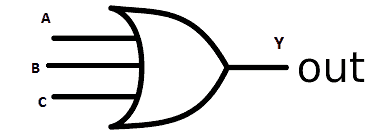
Logic OR gates can have ‘n’ number of inputs, which means it can have more than two inputs (Logic OR gates will have at-least two input and always one output).
For a 3 input logic OR gate the Boolean equation turns like this: (A + B + C) = Y, similarly for 4 input and above.
Truth Table for 3 input logic OR gate:
A (INPUT) | B (INPUT) | C (INPUT) | Y (OUTPUT) |
0 | 0 | 0 | 0 |
0 | 0 | 1 | 1 |
0 | 1 | 0 | 1 |
0 | 1 | 1 | 1 |
1 | 0 | 0 | 1 |
1 | 0 | 1 | 1 |
1 | 1 | 0 | 1 |
1 | 1 | 1 | 1 |
Multi Input Logic OR Gates:
Commercially available Logic OR gates are only available in 2, 3 and 4 inputs. If we have more than 4 input then we have to cascade the gates.
We can have six input logic OR gate by cascading the 2 input OR gates as follows:
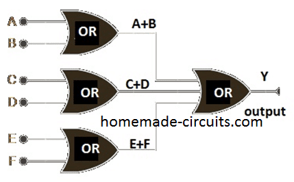
Now the Boolean equation for the above circuit becomes Y = (A+B)+(C+D)+(E+F)
Still, all the mentioned logical rules apply to the above circuit.
If you are going to use only 5 inputs from the above 6 inputs OR gate, we can connect a pull-down resistor at any one pin and now it becomes 5 input OR gate.
Transistor Based two input Logic OR gate:
Now we know, how a logic OR gate functions, let’s construct a 2 input OR gate using two NPN transistors. The logic ICs are constructed in the almost same the same way.
Two Transistor OR gate Schematic:
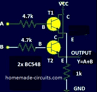
At the output “Y” you can connect a LED; if the output is high the LED will glow (LED +Ve terminal at “Y” with 330 ohm resistor and negative to GND).
When we apply LOW signal to the base of the two transistors, both the transistors turns OFF, the ground signal will be available at the emitter of the T2 / T1 via 1k pull-down resistor, thus the output turns LOW.
If any one of the transistor is ON, positive voltage will be available at emitter of T2 / T1, thus the output turns HIGH.
Now you know how to construct logic OR gate of your own.
Quad OR gate IC 7432:
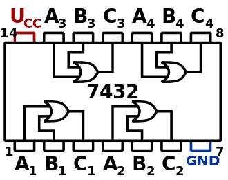
If you want to buy logic OR gate from the market, you will get in the above configuration.
It has 14 pins; the pin #7 and pin #14 are GND and Vcc respectively. It is operated at 5V.
Propagation delay:
Propagation delay is the time taken for the output to change from LOW to HIGH and vice versa.
The propagation delay from LOW to HIGH is 7.4 nanoseconds at 25 degree Celsius.
The propagation delay from HIGH to LOW is 7.7 nanoseconds at 25 degree Celsius.
• 74LS32 Quad 2-input
• CD4071 Quad 2-input
• CD4075 Triple 3-input
• CD4072 Dual 4-input
Logic Exclusive –OR Gate
In this post I am going to explain about logic XOR gate or Exclusive-OR gate. We will be taking a look at the basic definition, symbol, truth table, XOR equivalent circuit, XOR realization using logic NAND gates and finally, we will be taking overview on quad 2 input Ex-OR gate IC 7486.
In the previous posts, I have explained about three fundamental logic gates “AND”, “OR” and “NOT”. We also learned that, using these three fundamental gates we can construct two new logic gates “NAND” and “NOR”.
There are two more logic gates although these two are not basic gates but, it is constructed by the combination of the other logic gates and its Boolean equation is so vital and very useful that it is considered as distinct logic gates.
These two logic gates are “Exclusive OR” gate and “Exclusive NOR”. In this post we are going to only explore about logic Exclusive OR gate.
What is “Exclusive OR” gate?
It is an electronic gate, whose output turns “high” or “1” or “true” or gives out a “positive signal” when the two logic inputs are different with respect to each other (this is applicable only for two 2 input Ex-OR gate).
For example: Say an Exclusive OR gate with ‘two’ inputs, if one of the input pin A is “HIGH” and the input pin B is “LOW” then the output turns “HIGH” or “1” or “true” or “positive signal”.
If the both the inputs are same logic level i.e. both pins “HIGH” or both pins “LOW” the output turns “LOW” or “0” or “false” or “negative signal”.
Note:
The term “High”, “1”, “positive signal”, “true” are essentially the same (Positive signal is the battery’s or power supply’s positive signal).
The term “LOW”, “0”, “negative signal”, “false” are essentially the same (Negative signal is the battery’s or power supply’s negative signal).
Illustration of Logic Exclusive OR gate:
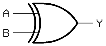
Here the “A” and “B” are the two inputs and the “Y” is output.
The Boolean expression for logic Ex-OR gate: Y = (A.) ̅B+A.B ̅
If ‘A’ is ‘1’ and ‘B’ is ‘1’ the output is (A ̅.B+A.B ̅) = 0 x 1 + 1 x 0 = ‘1’ or “LOW”
If ‘A’ is ‘0’ and ‘B’ is ‘1’ the output is (A ̅.B+A.B ̅) = 1 x 1 + 0 x 0 = ‘1’ or “HIGH”
If ‘A’ is ‘1’ and ‘B’ is ‘0’ the output is (A ̅.B+A.B ̅) = 0 x 0 + 1 x 1= ‘1’ or “HIGH”
If ‘A’ is ‘0’ and ‘B’ is ‘0’ the output is (A ̅.B+A.B ̅) = 1 x 0 + 0 x 1 = ‘0’ or “Low”
The above conditions are simplified in the truth table.
Truth Table (Two Input):
A (Input) | B (INPUT) | Y (Output) |
0 | 0 | 0 |
0 | 1 | 1 |
1 | 0 | 1 |
1 | 1 | 0 |
In the above two input logic Ex-OR gate, if the two inputs are different i.e. “1” and “0” the output turns “HIGH”. But with 3 or more input logic Ex-OR or in general the Ex-OR’s output turns “HIGH” only when the ODD number of logic “HIGH” is applied to the gate.
For example: If we have 3 input Ex-OR gate, if we apply logic “HIGH” to only one input (odd number of logic “1”) the output turns “HIGH”. If we apply logic “HIGH” to two inputs (this is even number of logic “1”) the output turns “LOW” and so on.
3 Input Exclusive OR Gate:
Illustration of 3 input EX-OR gate:
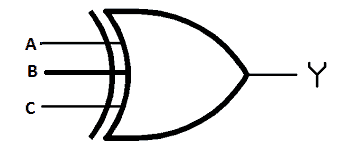
Truth Table for 3 input logic EX-OR gate:
A (INPUT) | B (INPUT) | C (INPUT) | Y (OUTPUT) |
0 | 0 | 0 | 0 |
0 | 0 | 1 | 1 |
0 | 1 | 0 | 1 |
0 | 1 | 1 | 0 |
1 | 0 | 0 | 1 |
1 | 0 | 1 | 0 |
1 | 1 | 0 | 0 |
1 | 1 | 1 | 1 |
For the 3 input Ex-OR gate the Boolean equation becomes: A(BC) ̅ + A ̅BC ̅ + (AB) ̅C + ABC
As we described before, the logic “Ex-OR” gate is not a fundamental logic gate but, combination of different logic gates. The Ex-OR gate can be realized using logic “OR” gate, logic “AND” gate and logic “NAND” gate as follows:
Equivalent circuit for “Exclusive OR” gate:
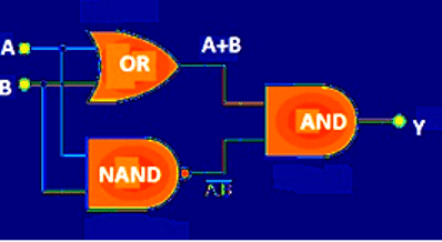
The above design has major drawback, we need 3 different logic gates to make one Ex-OR gate. But we can overcome this problem by implementing Ex-OR gate with only logic NAND gates, this is also economical to fabricate.
Exclusive OR gate using NAND gate:
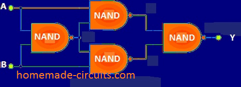
Exclusive OR gates are used to perform complicated computing tasks such as arithmetic operations, full adders, half-adders, it can also deliver carry out functionality.
Logic Exclusive OR Gate IC 7486:
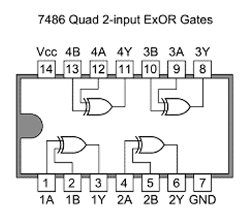
If you want to buy logic Ex-OR gate from the market, you will get in the above DIP configuration.
It has 14 pins; the pin #7 and pin #14 are GND and Vcc respectively. It is operated at 5V.
Propagation delay:
Propagation delay is the time taken for the output to change from LOW to HIGH and vice versa after giving input.
The propagation delay from LOW to HIGH is 23 nanoseconds.
The propagation delay from HIGH to LOW is 17 nanoseconds.
Commonly available “EX-OR” gate ICs:
- 74LS86 Quad 2-input
- CD4030 Quad 2-input
I hope the above detailed explanation might have helped you to understand regarding what logic gates are and how logic gates work, if you still have any questions? Please express in the comment section, you may get a quick reply.
नमस्ते, can you please help me?
I am using a logic gate, MU4SU69G2-TR with a micro switch to power it with 5 volts. The micro switch only closes for 2 milli seconds… Not enough time to keep the gate activated.. Is there a micro switch that can close for about 1 second? Or, is there a way to send voltage to the gate using this switch together with another small circuit with possibly a capacitor and transistor. Thank you in advance… Sew Sewram…. Please send me an email with your suggestion..