The transistorized low dropout voltage regulator circuit ideas explained in the following article can be used for getting stabilized output voltages right from 3 V and above, such as 5 V, 8 V, 9 V, 12 V, etc with an extremely low dropout of 0.1 V.
For example, if you make the proposed 5 V LDO circuit, it will continue to produce an output of a constant 5 V even if the input supply is as low as 5.1 V
Better than the 78XX Regulators
For the standard 7805 regulator we find that they compulsorily need a minimum of 7 V to produce a precise 5 V output, and so on. Meaning the dropout level is 2 V which looks very high and undesirable for many applications.
The simple LDO circuits I have explained below can be considered better than the popular 78XX regulators like 7805, 7812 etc since they do not require the input supply to be 2 V higher than the intended output level, rather can work with outputs within 2% of the input.
In fact, for all linear regulators such as the 78XX or LM317, 338 etc the input supply must be 2 to 3 V higher than the interned stabilized output.
Designing 5 V Low Dropout Regulator
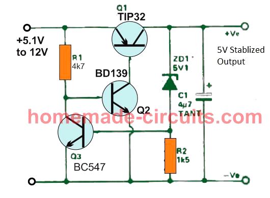
The figure above shows a simple low-dropout 5 V stabilized voltage regulator design that will give you a proper 5 V stabilized even when the input supply has dropped to less than 5.2 V.
The working of the regulator is actually very simple, Q1 and Q2 form a simple high gain common-emitter power switch, which allows the voltage to pass from the input to the output with a low dropout.
Q3 in association with the zener diode and R2 work like a basic feedback network which regulates the output to the value equivalent to the zener diode value (approximately).
This also implies that by changing the zener voltage value, the output voltage could be changed accordingly, as desired. This is an added advantage of the design since it enables the user to customize even the non-standard output values which are not available from the fixed 78XX ICs
Designing a 12 V Low Dropout Regulator
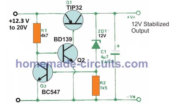
As explained in the previous section, merely changing the zener values change the output to the required stabilized level. In the above 12 v LDO circuit, we have replaced the zener diode with a 12 V zener diode to get a 12 V regulated output through inputs of 12.3 V to 20 V.
Current Specifications.
The current output from these LDO designs will depend on the value of R1, and the current handling capacity of Q1, Q2.
The indicated value of R1 will allow a maximum of 200 mA, which can be increased to higher amps by appropriately lowering the value of R1.
To ensure optimal performance, make sure that Q1, and Q2 are specified with high hFE, at least 50. Also, along with Q1 transistor, Q2 also must be a power transistor, as it might also get a bit hot in the process.
Short Circuit Protection
One apparent drawback of the explained low drop circuits is the lack of short circuit protection, which is normally a standard built-in feature in most normal fixed regulators.
Nevertheless, the feature can be added by including a current limiting stage using Q4 and Rx as shown below:
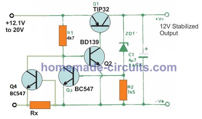
When the current increases beyond the predetermined limit, the voltage drop across Rx becomes sufficiently high to turn ON Q4, which begins grounding the Q2 base.
This causes Q1, Q2 conduction to become highly restricted, and the output voltage shuts down, until of course the current draw is restored to the normal level.
Low-Drop Transistor Regulator with Soft Start
This high gain voltage regulator using just a couple of transistors includes qualities better than those of the widely used multiple emitter-follower variants.
The circuit had been tried in a 30 watt stereo amplifier that strictly demanded a highly regulated supply and also an output voltage which could climb slowly and gradually through zero volts to maximum, whenever the circuit was initially powered up.
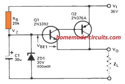
This soft-start plan (around 2 seconds) for the power amplifiers helped the 2000 uF output capacitors to charge without triggering too much collector current within the output transistors.
Normal regulator output impedance is 0.1 ohm. Output voltage is found by solving the equation by:
VO = VZ - VBE1.
The rise time of the output voltage is evaluated by calculating through the formula:
T = RB.C1(1 -Vz/V ).
A number of digital devices call for a preset switch on sequence for their power supplies. By establishing proper RB/C1 values, the rise time of the circuit's output could be fixed to deliver this sequence or delay interval.
Adjustable LDO Circuit
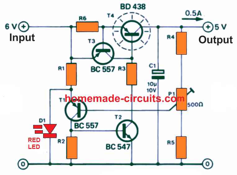
As can be in the schematic, the load is attached to the collector pin of the series transistor T4.
This indicates that this particular transistor could be turned ON hard into saturation, causing the voltage between emitter and collector to be just an extremely tiny saturation voltage.
This specific voltage level is dependent naturally on current specification and the type of the transistor.
Parts List
- R1 = 1.2 Ohms
- R2 = 10k
- R3 = 470 Ohms
- R4 = 1.2 k
- R5 = 560 Ohms
- R6 = 1.6 Ohms
- P1 = preset 500 Ohm
- C1 = 10uF/25V
- T1, T3 = BC557
- T2 = BC547
- T4 = BD438
- LED = RED 20mA 5mm
In the case of the discussed design considering a optimum current of 0.5 A the voltage drop will probably be hardly 0.2 V.
Combine with this the voltage drop around R6, necessary for current limiting. With roughly 0.5 V across R6, T3 begins conducting and restricts the output current.
LED D1 possesses a couple of functions, it works as an indicator and also as a voltage reference diode in order to clamp a 1.5 V to 1.6 V refernce level at the emitter of T1.
The base drive current for T1 comes from the voltage divider which involves R4, P1 and R5. With respect to the difference between the reference and output voltage levels, T1 slowly starts conducting.
Exactly the same then happens with T2 which provides more or less base drive to T4. The function of capacitor C1 is to filter the output stage.
You can easily replacing BD 438 with other popular brands, for example like BD136, BD138 and BD140 etc.
Having said that, these transistors may likely posses a rather increased saturation voltage. It should be observed that because D1 works like a reference source, it should be be a red-colored LED, other color LEDs may have other voltage drop specifications.
How to Design a Low Dropout Voltage Regulator using Transistors
Contributed by : Carl
I needed a voltage regulator with an extremely low dropout voltage, capable of delivering a stable 5 V at approximately 3 A. Since numerous three-terminal regulators possess a dropout of 2.5 V or more, I designed the LDO circuit described below employing discrete components.
Although fairly straightforward, this low dropout voltage regulator design demonstrated performance on par with that of integrated circuit (IC) regulators.
The schematic of the prototype is displayed in the Figure below, yielding the subsequent test outcomes:
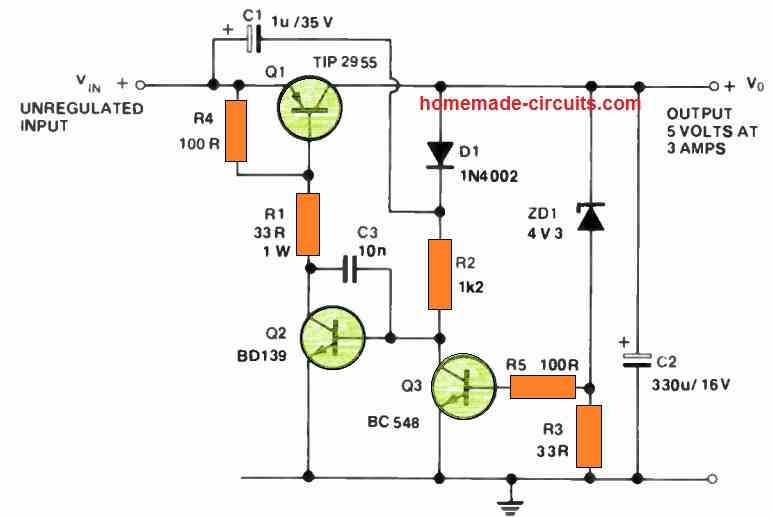
- Dropout voltage (@ 3 A): 0.75 V
- Load Regulation (0-3 A): Below 10 mV
- Line regulation (Vin 6 — 15 V): Below 10 mV
- Ripple rejection (@ 3 A): -63 dB
- Output (no load): 4.96 V
Alterations in the output voltage resulting from shifts in ambient temperature will primarily hinge on the traits of the zener diode, ZD1, and transistor Q3.
Consequently, it is imperative to maintain these elements away from heat sources, such as the heatsink for Q1 and the power transformer.
As the current configuration of the circuit currently lacks a precisely defined current limit, this capability can be incorporated by integrating the components portrayed in the Figure below.
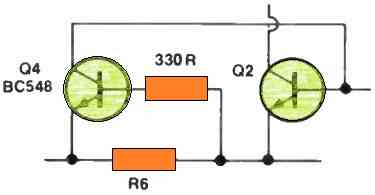
However, doing so will result in a 0.5 V increase in the dropout voltage. Alternatively, you can establish a current limit without heightening the dropout voltage by loading the output to the desired maximum current and incrementally augmenting the value of resistor R1 until the output voltage starts to decline.
The downside of this method is that RI must be chosen through experimentation and may necessitate recalibration if Q1 is ever replaced.
Consequently, if a current limit is imperative and a minor elevation in dropout voltage is tolerable, the procedure depicted in the second figure above is the preferred choice.
Another noteworthy trait of this circuit is its capacity to automatically deactivate should a substantial load cause the output voltage to plunge beneath roughly 1.2 V.
To restart it, you must disengage the input voltage (or power down the mains), wait several seconds, and then reapply power. Simply unburdening the load will not enable a restart.
Components C1 and D1 serve as inception components, ensuring dependable starts even with markedly capacitive loads.
To adapt the circuit for varying voltage and current requisites (up to approximately 5 A), adhere to this streamlined design methodology:
- Determine the output voltage, Vo (5 V).
- Elect the maximum current, Io (3 A).
- Choose a fitting transistor for Q1 (TIP2955, 70 V, 10 A).
- Calculate R1 max: Vo / (Io / (Q1 hFE)) = 5 / (3 / 20) = 33.3 ohms or simply 33 ohms.
- Compute the dissipation of R1: Vo^2 / R1 = 25 / 33 = 0.75 W (employ a 1 W resistor).
- Select an appropriate device for Q2 (BD139, 80 V, 1 A).
- Determine R2 max: Vo / (Io / (Q1 hFE) * (Q2 hFE)) = 5 / (3 / 20 * 40) = 1300 ohms; employ a 1k2 resistor.
- Assess the dissipation of R2: Vo^2 / R2 = 25 / 1200 = 21 mW.
- Choose an apt device for Q3 (BC548, 25 V, 100 mA).
- Pick a zener diode, ZD1, possessing a voltage of Vo - Vbe (Q3) = 5 - 0.65 = 4.35 V (utilize a 4V3 zener). As the current coursing through Q3's base typically remains minute, a low-wattage 400 mW or 1 W zener can be utilized.
- Compute R3 to bias the zener: I2 = 0.2 * (P2 / V2) = 0.2 * (0.4 / 4.3) (assuming a 400 mW zener) = 18.6 mA. Ergo, R3 = 0.65 V / 18.6 mA = 35 ohms (use a 33-ohm, 1/4 W resistor).
- R4 serves to forestall Q1 from activating due to leakage; its precise value is not crucial, and a 100-ohm, 1/4 W resistor is generally fitting.
- R5 serves as a precautionary measure to confine excessive current through Q3's base and can be 100 ohms.
- C1 serves as the startup capacitor, and any capacity between 1 uF and 4.7 uF should suffice, with a voltage rating surpassing Vin.
- C2 is employed for stability, with an appropriate value being 100 uF per amp of load current. A 330 uF capacitor was employed in the prototype, and its voltage rating should exceed the output voltage rating.
- C3 is indispensable for stability and should be around 10 nF.
- Mount Q1 on an appropriate heatsink, contingent on the power it dissipates, which should be modest if Vin-Vout is low.