A relatively simple 1000 watt pure sine wave inverter circuit is explained here using a signal amplifier and a power transformer.
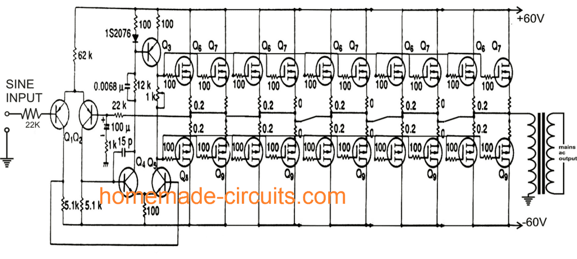
As can be seen in the first diagram below, the configuration is a simple mosfet based designed for amplifying current at +/-60 volts such that the connected transformer corresponds to generate the required 1kva output.
UPDATE:
There's a much easier and efficient way of making a 1 kva inverter circuit using the following 4017 PWM version circuit. Since the PWM is created directly through the 4017 output, the PWMs are much accurate and the waveform is uniform and does not depend on any external adjustments.
The biggest advantage of using this circuit is that the output can be modified to almost a pure sine wave by adding a few PPC capacitors across the transformer output.
Here' the circuit which you can try:
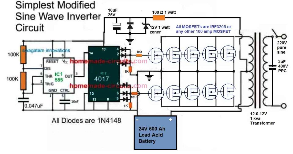
Parts List
- Resistors
- All resistors are 1/4 watt 5% unless specified
- 100K = 2nos
- 100 ohm 1 watt = 1no
- 1K = 2no
- 10 ohm = 2no
- Capacitors
- 0.047uF ceramic or PPC = 1no
- 10nF ceramic or PPC = 1no
- 10uF/25V Electrolytic = 1no
- Semiconductors
- 1N4148 diodes = 7nos
- 12V/1 watt zener diode = 1no
- IRF3205 MOSFETs = 10nos
- Transformer 12-0-12V/220V/1kva
- Battery = 24V/500 Ah = 1no
The previous original article which is continued in the following paragraphs also discusses a 1000 watt inverter circuit, however, this circuit being a linear amplifier is not so efficient, and may result in a lot of dissipation.
I would recommend trying the above circuit, which will give you a 100% results quickly.
Remember, you must first try and confirm the working of the inverter using single MOSFETs on each channel. Once the working is confirmed then you can add more number of MOSFETs in parallel to upgrade the power capacity of the inverter to 1000 watts
Circuit Operation
Q1, Q2 forms the initial differential amplifier stage which appropriately raises the 1vpp sine signal at its input to a level which becomes suitable for initiating the driver stage made up of Q3, Q4, Q5.
This stage further raises the voltage such that it becomes sufficient for driving the mosfets.
The mosfets are also formed in the push pull format, which effectively shuffles the entire 60 volts across the transformer windings 50 times per second such that the output of the transformer generates the intended 1000 watts AC at the mains level.
Each pair is responsible for handling 100 watts of output, together all the 10 pairs dump 1000 watts into the transformer.
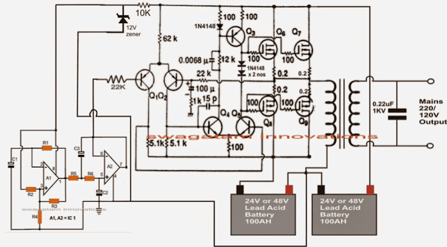
For acquiring the intended pure sine wave output, a suitable sine input is required which is fulfilled with the help of a simple sine wave generator circuit.
It is made up of a couple of opamps and a few other passive parts. It must be operated with voltages between 5 and 12. This voltage should be suitably derived from one of the batteries which are being incorporated for driving the inverter circuit.
The inverter is driven with voltages of +/-60 volts that amounts to 120 V DC.
This huge voltage level is obtained by putting 10 nos. of 12 volt batteries in series.
The Sinewave Generator Circuit
The below given diagram shows a simple sine wave generator circuit which may be used for driving the above inverter circuit, however since the output from this generator is exponential by nature, might cause a lot of heating of the mosfets.
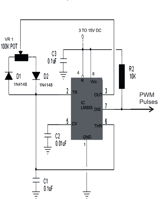
A better option would be to incorporate a PWM based circuit which would supply the above circuit with appropriately optimized PWM pulses equivalent to a standard sine signal.
The PWM circuit utilizing the IC555 has also been referred in the next diagram, which may be used for triggering the above 1000 watt inverter circuit.
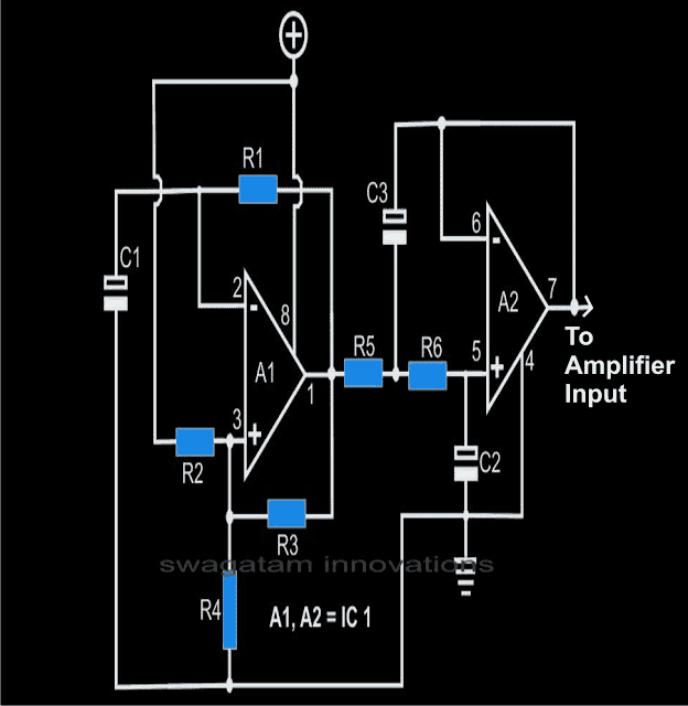
Parts List for the sine generator circuit
All resistors are 1/8 watts, 1%, MFR
R1 = 14K3 (12K1 for 60Hz),
R2, R3, R4, R7, R8 = 1K,
R5, R6 = 2K2 (1K9 for 60Hz),
R9 = 20K
C1, C2 = 1µF, TANT.
C3 = 2µF, TANT (TWO 1µF IN PARALLEL)
C4, C6, C7 = 2µ2/25V,
C5 = 100µ/50v,
C8 = 22µF/25V
A1, A2 = TL 072
Part List for Inverter
Q1, Q2 = BC556
Q3 = BD140
Q4, Q5 = BD139
All N-channel mosfet are = K1058
All P-channel mosfets are = J162
Transformer = 0-60V/1000 watts/output 110/220volts 50Hz/60Hz
The proposed 1 kva inverter discussed in the above sections can be much streamlined and reduced in size as given in the following design:
How to Connect Batteries
The diagram also shows the method of connecting the battery, and the supply connections for the sine wave or the PWM oscillator stages.
Here just four mosfets have been used which could be IRF4905 for the p-channel, and IRF2907 for n-channel.
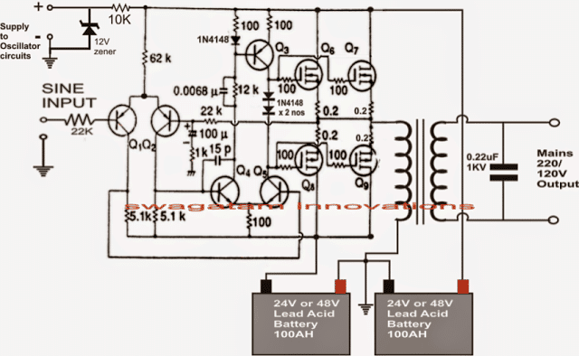
Complete 1 kva inverter circuit design with 50 Hz sine oscillator
In the above section we have learned a full bridge design in which two batteries are involved for accomplishing the required 1kva output. Now let's investigate how a full bridge design could be constructed using 4 N channel mosfet and using a single battery.
The following section shows how a full-bridge 1 KVA inverter circuit can be built using, without incorporating complicated high side driver networks or chips.
Using Arduino
The above explained 1kva sinewave inverter circuit can be also driven through an Arduino for achieving almost a prefect sinewave output.
The complete Arduino based circuit diagram can be seen below:
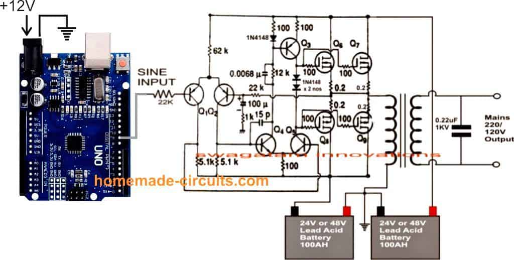
Program Code is given below:
//code modified for improvement from http://forum.arduino.cc/index.php?topic=8563.0

//connect pin 9 -> 10k Ohm + (series with)100nF ceramic cap -> GND, tap the sinewave signal from the point at between the resistor and cap.

float wav1[3];//0 frequency, 1 unscaled amplitude, 2 is final amplitude

int average;

const int Pin = 9;

float time;

float percentage;

float templitude;

float offset = 2.5; // default value 2.5 volt as operating range voltage is 0~5V

float minOutputScale = 0.0;

float maxOutputScale = 5.0;

const int resolution = 1; //this determines the update speed. A lower number means a higher refresh rate.

const float pi = 3.14159;

void setup() {

wav1[0] = 50; //frequency of the sine wave

wav1[1] = 2.5; // 0V - 2.5V amplitude (Max amplitude + offset) value must not exceed the "maxOutputScale"

TCCR1B = TCCR1B & 0b11111000 | 1;//set timer 1B (pin 9) to 31250khz

pinMode(Pin, OUTPUT);

//Serial.begin(115200);//this is for debugging

}

void loop() {

time = micros()% 1000000;

percentage = time / 1000000;

templitude = sin(((percentage) * wav1[0]) * 2 * pi);

wav1[2] = (templitude * wav1[1]) + offset; //shift the origin of sinewave with offset.

average = mapf(wav1[2],minOutputScale,maxOutputScale,0,255);

analogWrite(9, average);//set output "voltage"

delayMicroseconds(resolution);//this is to give the micro time to set the "voltage"

}

// function to map float number with integer scale - courtesy of other developers.

long mapf(float x, float in_min, float in_max, long out_min, long out_max)

{

return (x - in_min) * (out_max - out_min) / (in_max - in_min) + out_min;

}
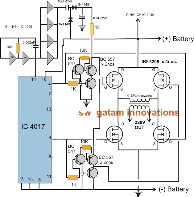
The Full-Bridge Inverter Concept
Driving a full bridge mosfet network having 4 N-channel mosfets is never easy, rather it calls for reasonably complex circuitry involving complex high side driver networks.
If you study the following circuit which has been developed by me, you will discover that after all it's not that difficult to design such networks and can be done even with ordinary components.
We will study the concept with the help of the shown circuit diagram which is in the form of a modified 1 kva inverter circuit employing 4 N-channel mosfets.
As we all know, when 4 N-channel mosfets are involved in an H-bridge network, a bootstrapping network becomes imperative for driving the high side or the upper two mosfets whose drains are connected to the high side or the battery (+) or the positive of the given supply.
In the proposed design, the bootstrapping network is formed with the help of six NOT gates and a few other passive components.
The output of the NOT gates which are configured as buffers generate voltage twice that of the supply range, meaning if the supply is 12V, the NOT gate outputs generate around 22V.
This stepped up voltage is applied to the gates of the high side mosfets via the emitter pinouts of two respective NPN transistors.
Since these transistors must be switched in such a way that diagonally opposite mosfets conduct at a time while the the diagonally paired mosfets at the two arms of the bridge conduct alternately.
This function is effectively handled by the sequential output high generator IC 4017, which is technically called Johnson divide by 10 counter/divider IC.
The Bootstrapping Network
The driving frequency for the above IC is derived from the bootstrapping network itself just to avoid the need of an external oscillator stage.
The frequency of the bootstrapping network should be adjusted such that the output frequency of the transformer gets optimized to the required degree of 50 or 60 Hz, as per the required specs.
While sequencing, the outputs of the IC 4017 trigger the connected mosfets appropriately producing the required push-pull effect on the attached transformer winding which activates the inverter functioning.
The PNP transistor which can be witnessed attached with the NPN transistors make sure that the gate capacitance of the mosfets are effectively discharged in the course of the action for enabling efficient functioning of the entire system.
The pinout connections to the mosfets can be altered and changed as per individual preferences, this might also require the involvement of the reset pin#15 connection.
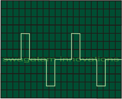
Waveform Images
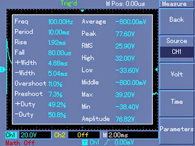
The above design was tested and verified by Mr. Robin Peter one of the avid hobbyists and contributor to this blog, the following waveform images were recorded by him during the testing process.


