In the following post I have explained a pure sine wave inverter circuit using the IC 556 which forms the main sine wave processor device in the circuit.
How it Works
The presented design actually produces a modified sine wave output, but the waveform is highly processed and constitutes an exact equivalent of a sinusoidal waveform.
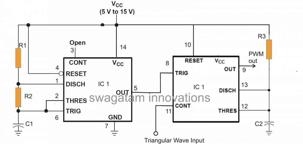
A single IC 556 forms the heart of the circuit and is responsible for manufacturing the required PWM controlled modified sine output waveform.
One half of the IC on the left is configured as a 200Hz frequency generator, this frequency is used for providing the required square wave clocks to the preceding monostable which is formed by wiring up the other half of the 556 IC.
The clocks are received from pin#5 and applied to pin#8 of the IC. The right hand side section of the IC does the actual processing of the above square wave by comparing it to the triangular waves applied at its pin#11.
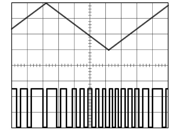
The result is an output at pin#9 which is a PWM, varying in accordance with the amplitude of the triangular waveform.
Ideally the triangular waves can be replaced with a sine waveform, however since triangular waves are easier to generate, and also appropriately replaces the sine counterpart, its been employed here.
R1, R2, C1 should be appropriately selected so that pin#5 produces a 50% duty cycle, 200 Hz frequency.
The 200 Hz is not critical here, however it becomes critical for the IC 4017 stage and that's why it's been selected to that value.
The modified sine wave PWM generated by the IC556 is next applied to the switching stage comprising the IC 4017 and the relevant output mosfet devices. Let's see how it's done.

Parts List
IC1 = 556
R1,R2,C1 = select to generate 50% duty cycle
R3 = 1K
C2 = 10pF.

The output stage
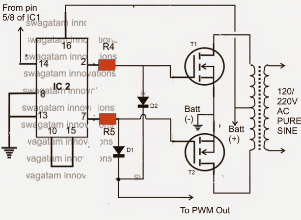
The diagram given below shows the output stage configuration where the IC 4017 takes the center stage. Basically its function is to switch the driver transistors alternately so that the connected mosfets also conduct in tandem for inducing the required mains AC output into the transformer.
The IC receives the clock pulses from the above explained 556 circuit (pin#5/8) and its outputs sequence across the connected transistors alternately as discussed above.
Until here the circuit behaves like an ordinary square wave inverter, however the introduction of D1/D2 with the pin#9 of the 556 transforms the circuit into a full fledged pure sine wave inverter.
As can be seen, the common cathodes of D1/D2 are integrated with the processed PWM pulses from the above 556 stage, this forces D/D2 to conduct only during the negative pulses from the generated PWM blocks.
It simply means that when D1/D2 are forward biased, T1 and T2 are inhibited from conducting since their gates become grounded through D1/D2 into pin#9 of the IC 556, which make the mosfets respond exactly to the PWM pattern.
The above process generates an output across the transformer secondary that's perfectly chopped and processed and equivalent to a sine waveform.

Parts List
IC2 = 4017
all resistors are 1K
D1,D2 = 1N4148
T1,T2 = IRF540n
Transformer should be also appropriately rated as per the requirement.
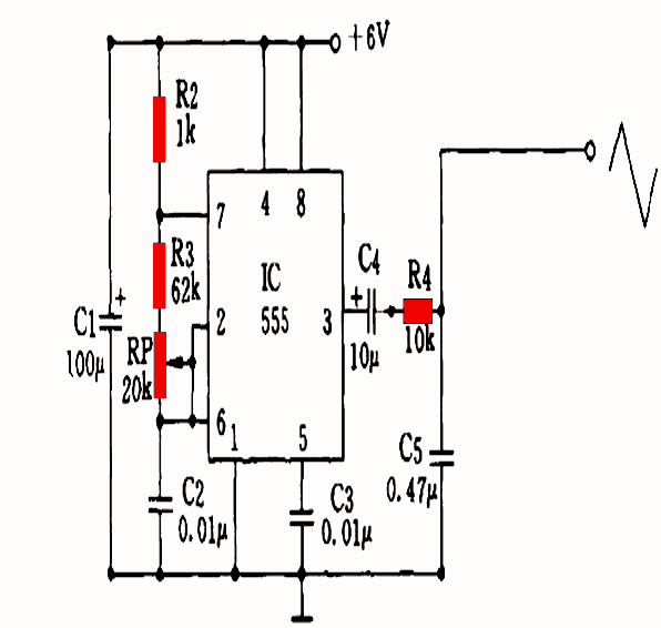
The Triangular Wave Generator Circuit
The entire modified sine PWM waveform construction and implementation is dependent on the fed triangular waves at pin#11 of the IC556, therefore a triangle wave generator circuit becomes crucial and imperative.
However there are many types circuits that will provide you with the required waveform inputs, the following is one of them which incorporates yet another IC555 and is pretty simple to configure.
The output from the below given circuit must be fed to pin#11 of the IC556 for enabling the proposed sine wave inverter functioning.

DESIGNED BY "SWAGATAM"
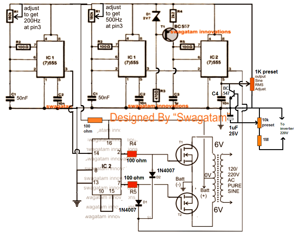
A simpler alternative to the above design is shown below, the configuration would produce same results as explained above: