
In this brief tutorial I have explained how to design a customized UPS circuit at home using ordinary components such as a few NAND ICs and a some relays.
What is an UPS
UPS which stands for uninterruptible power supply are inverters designed to provide a seamless AC mains power to a connected load without a slightest bit of interruption, regardless of sudden power failures or fluctuation or even a brown-out.
An UPS becomes useful for PCs and other such equipment which involve critical data handling and cannot afford mains power interruption during a vital data processing operation.
For these equipment UPS becomes very handy due to its instantaneous power back-up to the load, and for providing the user with ample time to save computer's crucial data, until actual mains power is restored.
This means that an UPS must be extremely quick with its changeover from mains to inverter (back up mode) and vice versa during a possible mains power malfunction.
In this article I have explained how to make a simple UPS with all the bare minimum features, ensuring that it conforms with the above fundamentals and provides the user with a good quality uninterrupted power throughout the course of its operations.
UPS Stages
A basic UPS circuit will have the following fundamental stages:
1) An inverter circuit
2) A Battery
3) A battery charger circuit
4) A changeover circuit stage using relays or other devices such as triacs or SSRs.
Now I have explained how the above circuit stages may be built and integrated together for implementing a reasonably decent UPS system.
Block Diagram
The mentioned functional stages of an uninterruptible power supply unit could be understood in detail through the following block diagram:

Here we can see that the main UPS changeover function is carried out by a couple of DPDT relay stages.
Both the DPDT relays are powered from a 12 V AC to DC power supply or adapter.
The left side DPDT relay can be seen controlling the battery charger. The battery charger gets powered when AC mains is available through the upper relay contacts, and supplies the charging input to the battery via the lower relay contacts. When AC mains fails, the relay contacts changeover to the N/C contacts. The upper relay contacts switches OFF power to the battery charger, while the lower contacts now connects the battery with the inverter to initiate the inverter mode operation.
The right side relay contacts are used for changing over from grid AC mains to the inverter AC mains, and vice versa.
A Practical UPS Design
In the following discussion I will try to explain and design a practical UPS circuit.
1) The Inverter.
Since an UPS has to deal with crucial and sensitive electronic appliances, the involved inverter stage must be reasonably advanced with its waveform, in other words an ordinary square wave inverter may not be recommended for an UPS, and therefore for our design we make sure that this condition is aptly taken care of.
Although I have posted many inverter circuits in this website, including sophisticated PWM sinewave types, here we select a completely new design just to make the article more interesting, and add a new inverter circuit in the list
The UPS design utilizes just a single IC 4093 and yet is able to execute a good PWM modified sine wave functions at the output.
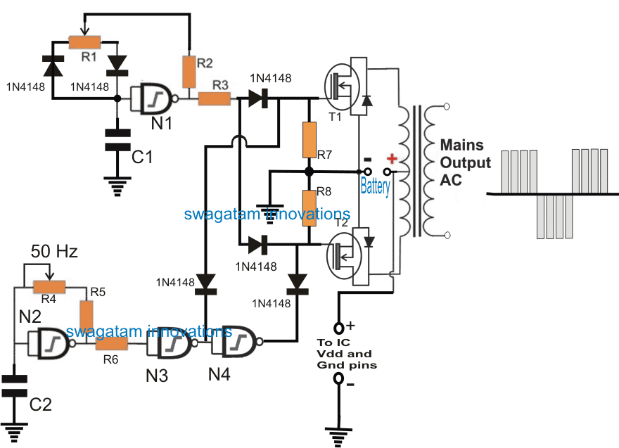
Parts List
- N1---N3 NAND gates from IC 4093
- Mosfets = IRF540
- Transformer = 9-0-9V / 10 amps / 220V or 120V
- R3/R4 = 220k pot
- C1/C2 = 0.1uF/50V
- All resistors are 1K 1/4 watt
Inverter Circuit Operation
The IC 4093 consists of 4 Schmidt type NAND gates, these gates are appropriately configured and arranged in the above shown inverter circuit, for implementing the required specifications.
One of the gates N1 is rigged as an oscillator to produce 200 Hz, while another gate N2 is wired as the second oscillator for generating 50Hz pulses.
The output from N1 is used for driving the attached mosfets at the rate of 200Hz while the the gate N2 along with the additional gates N3/N4, switches the mosfets alternately at the rate of 50Hz.
This is to ensure that the mosfets are never allowed to conduct simultaneously from the output of N1.
The outputs from N3, N4 break the 200Hz from N1 into alternate blocks of pulses which are processed by the transformer to produce a PWM AC at the intended 220V.
This concludes the inverter stage for our UPS making tutorial.
The next stage explains the changeover relay circuit, and how the above inverter needs to be wired with the changeover relays for facilitating the automatic inverter back up and battery charging operations during mains failure, and vice versa.
Relay Changeover Stage and Battery Charger Circuit
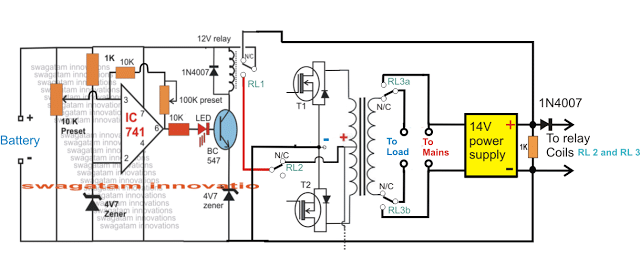
The image below shows how the transformer section of the inverter circuit may be configured with a few relays for implementing the automatic changeover for the proposed UPS design.
The figure also shows a simple automatic battery charger circuit using the IC 741 on the left side of the diagram.
First I have explained how the changeover relays are wired and then we can proceed with the battery charger explanation.
In all there are 3 sets of relays which are used in this stage:
1) 2 nos of SPDT relays in the form of RL1 and RL2
2) One DPDT relay as RL3a and RL3b.
RL1 is attached with the battery charger circuit and it controls the high/low cut charge level cut-off for the battery and determines when the battery needs is ready to be used for the inverter and when it needs to be removed.
The SPDT RL2 and the DPDT (RL3a and RL3b) are used for the instant changeover actions during a power failure and restoration. RL2 contacts are used for connecting or disconnecting the center tap of the transformer with the battery depending on the mains availability or absence.
RL3a and RLb which are the two sets of contacts of the DPDT relay become responsible for switching the load across the inverter mains or the grid mains during power outages or restoration periods.
The coils of RL2 and DPDT RL3a/RL3b are joined with a 14V power supply such that these relays quickly activate and deactivate depending on the input mains status and do the necessary changeover actions. This 14V supply is also used as the source for charging the inverter battery while the mains power is available.
The coil of the RL1 can be seen connected with the opamp circuit which controls the battery charging of the battery and ensures the supply to the battery from the 14V source is cut-off as soon as it reaches the same value.
It also makes sure that while the battery is in the inverter mode and is consumed by the load, its lower discharge level never goes below 11V, and it cuts off the battery from the inverter when it reaches around this level. Both these operations are executed by the relay RL1 in response to the opamp commands.
The setting-up procedure for the above UPS battery charger circuit can be learned from this article which discuses how to make a low high cut off battery charger using IC 741
Now it simply needs to integrate all the above stages together for executing a decent looking small UPS, which could be used for providing an uninterruptible power to your PC or any other similar gadget.
That's it, this concludes our tutorial for designing a personal UPS circuit which can be easily done by any new hobbyist by following the above detailed guide.