Today the traditional wired type of doorbells are gradually getting obsolete and are being replaced by the advanced wireless type of doorbells that are easier to install due to their hassle free set-ups. A simple wireless doorbell circuit is discussed in the following post which can be constructed at home.

Written and Submitted By: Mantra
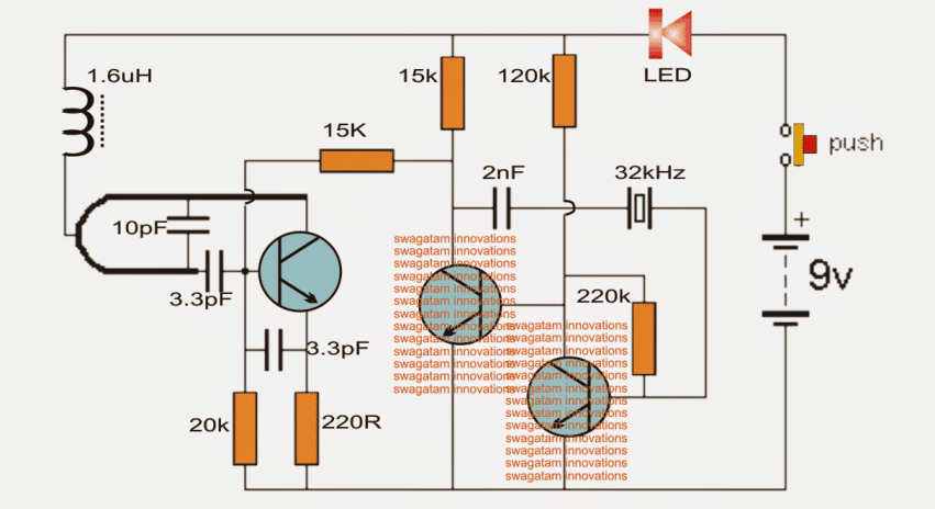
303MHz TRANSMITTER with 32kHz Crystal
The initial circuit we are going to explore has a 32kHz crystal to crank out a tone which means that the receiver is unable to false-trigger.
We could perhaps experience a fault with the commercial RX-3 circuits every 2 minutes, this might be due to the chip detecting a frequency of 1kHz or 250Hz from the environment disturbance received by the RF transistor, to turn on an output.
That's exactly why the RX-3 receiver chip is untrustworthy. A 32kHz is a much better frequency to identify because it does not get rattled from environment resonance.
The functionality of a 303MHz circuit has been covered in this project WIRELESS DOORBELL.
We are not going over how the circuit works but explain the importance of some of the components and how they effect the range.
The Wireless Doorbell transmitter and receiver circuit are incorporated below:

All Transistors are 2N3563, the U shape coil is a single half turn using a 1mm copper wire with 5mm diameter
The most fundamental constituent is the transistor.
An excellent transistor is critical in the RF phase and the Japanese transistors are undoubtedly suits this objective.
The transistor employed in the 303MHz oscillator possesses an optimum frequency for the functionality of 1,000MHz in this most assuredly is where the gain is equal to "1," therefore we would like a transistor to have a unique gain at 300MHz.
A BC 547 transistor is not going to function at this frequency as a result now we have considered a good choice a 2N 3563 that may be inexpensive which enables it to work with up to 1,000MHz. requirement papers when dealing with these transistors:
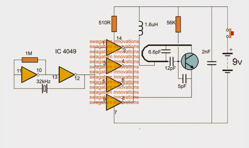
303MHz TRANSMITTER using 4049 IC
The following circuit works by using a CD 4049 IC to churn out the 32kHz frequency and four gates in parallel to transform the oscillator transistor on and off at the tone-rate.
An individual gate will not likely possess as much as necessary performance to suck the emitter to ground, nevertheless 4 gates will certainly bring along the emitter in close proximity to 0v rail.
It ought not be at specifically 0v as the 6p would not possess a direct impact in sustaining oscillation.
The IC bears 6 gates just in case an input is probably above mid rail, the output moves LOW.
Any time the input amounts to slightly below middle of the rail the output scales HIGH. The space between detecting a low and a high might not be massive as well as the gate will certainly pick up receptions referred to as "analogue signals."
However to obtain the oscillator circuit to startup, a resistor is positioned between output and input.
This will likely generate an oscillation at the maximum frequency for the gate roughly 500kHz to 2MHz..

All Transistors are 2N3563, the U shape coil is a single half turn using a 1mm copper wire with 5mm diameter
In case an additional gate is included along with a crystal hooked up between the output as well as the input, a "fight" transpires between the transmission coming from the 1M and the rate of recurrence transferred by the crystal.
Considering that the crystal possesses a reduced impedance as compared to the 1M, it accomplishes a more substantial signal to input pin 11 along with the 2 gates function at the frequency of the crystal.
The precise characteristics of the correct way the reception from the crystal overtakes the signal administered back from the 1M resistor is not critical in spite of this providing you can contemplate the first gate starts out to rise in frequency from nil, every time the signal reaches 32kHz, it commences to initialize the crystal which in turn forces the signal on the reverse side and into the input pin of the first gate.
Each transmitters churn out the identical outcomes, a 303MHz carrier with a 32kHz modulation (frequency - despite the fact that we are unable to perceive sound in this frequency). Each possess the matching spectrum.
The oscillator coil is furthermore the radiator of the signal as well as the 1.5uH inductor on the "centre tap" of the coil is often as high as 10uH or as little as 1.5uH, with minimal variance in output.
The frequency might well need to be realigned somewhat if the inductor is modified.
We transformed it for a forty turn air-would coil working with.25mm wire on a 2mm former. This amplified the distance by one metre.
Inductor Specifications
A sixty turn coil enhanced the range an additional 3 metres once it was subsequently expanded it added to the impact of the antenna. The pair of photos below exhibit the positioning of the air-inductors.
40 turn coil swapping the 1.5uH inductor. Sixty turn coil expanded to multiply the range of the wireless transmitter

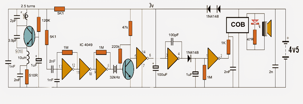
All Transistors are 2N3563, the antenna coil is 2.5 turns of 1mm copper wire over a 5mm variable slug assembly
303MHz RECEIVER
This doorbell is cheaper than $8.00 therefore it is impossible to get the components independently for lower than that.
This sort of circuit formulates an excellent groundwork for exhaustive study. It is possible to investigate the RF side of the circuit not to mention the high impedance segments.
Each gate includes promoting an extremely high gain and by applying a 1M from output to input the gate is saved in a state of stimulation, oscillating at approx 500kHz, in the event hardly any other parts encompass the gate to manage the frequency.
This could be formulated to retain the gate dynamic to ensure that the tiniest signal is going to be processed.
When it comes to the gate between pins 13 and 12, the 1n capacitor between the input and ground lessens the frequency significantly, in addition to the impact of the 2n2 as well as 5k6 resistor.
The 2nd and 3rd gates straightforwardly improve the amplitude of the signal and never render any specific version of elimination of undesired receptions.
The consequence is an entire amplitude signal at the left-side of the crystal together with all varieties hash and backdrop disturbance, then again aside from the signal features a 32kHz factor, it is going to not commence to oscillate and the right side would have no reception.
The crystal is the element that does nearly all of the "detection work" as well as inhibits misleading activating because it magically instincts out the 32kHz signal from the "hash" and produces an extremely unpolluted transmission to the transistor for in depth amplification.
This reception is heightened in conjunction with full rail as well as charges an electrolytic to actuate an audio chip.

Have Questions? Please Comment below to Solve your Queries! Comments must be Related to the above Topic!!