When an inverter with square wave AC output is modified to generate a crude sinewave AC output, it is called a modified sine wave inverter.
The following article presents 7 interesting modified sine wave inverter designs with exhaustive descriptions regarding its construction procedure, circuit diagram, waveform output and detailed parts lists. The designs are intended for learning and building experimental projects by engineers and students.
Here I have explained different varieties of modified designs ranging from a modest 100 watt to a massive 3 Kva power output model.
How Modified Inverters Work
Folks who are new to electronics may get a bit confused regarding the difference between a square wave and a modified square wave inverter. It may be understood through the following brief explanation:
As we all know an inverter will always generate an alternating current (AC) similar to our domestic AC line voltage so that it can replace it during power failures. An AC in simple words is basically a rise and fall of voltage of a particular magnitude.
However, ideally this AC is supposed to as close as possible to a sinewave as shown below:

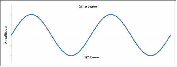
Basic Difference between Sine waveform and Square Waveform
This rise and fall of voltage happens at a particular rate i.e. at a particular number of times per second, known as its frequency. So for example a 50 Hz AC means 50 cycles or 50 ups and downs of a particular voltage in one second.
In a sine wave AC as found in our normal domestic mains outlet the above rise and fall of voltage is in the form of a sinusoidal curve, i.e. its pattern gradually varies with time and thus is not sudden or abrupt. Such smooth transitions in the AC waveform becomes very suitable and a recommended type of supply for the many common electronic gadgets like TVs , music systems , Refrigerators, motors etc.
However, in a square wave pattern the voltage ups and downs are instant and sudden. Such immediate rise and fall of potential creates sharp spikes at the edges of each wave and thus becomes very undesirable and unsuitable for sophisticated electronic equipment. Therefore it is always dangerous to operate them through a Square weave inverter supply.
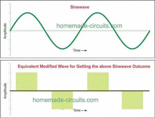
Modified Waveform
In a modified square wave design as shown above, the square waveform shape basically remains the same but the size of each section of the wave-form is appropriately dimensioned so that its average value matches closely to an AC waveform’s average value.
As you can see there's a proportionate amount of gap or null areas between each square blocks, these gaps ultimately help to shape up these square waves into sinewave like output (albeit crudely).
And what is responsible for adjusting these dimensioned square waves into sinewave like features? Well, it is the inherent characteristic of the transformer's magnetic induction which effectively carve the "dead time" transitions between the square wave blocks into a sinewave looking waves, as shown below:
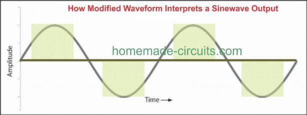
In all the 7 designs I have explained below we try to implement this theory and ensure that the RMS value of the square waves are appropriate controlled by chopping the 330V peaks into 220V modified RMS. The same can be applied for 120V AC by chopping down the 160 peaks.
How to Calculate through Easy Formulas
If you are interested to know how to calculate the above modified waveform so that it results in an almost ideal replication of a sinewave, then please refer to the following post for the complete tutorial:
Calculate Modified Square Wave RMS Sine Equivalent Value
Design#1: Using IC 4017
Let's investigate the first modified inverter design which is rather simple and uses a single IC 4017 for processing the required modified waveform.
If you are looking for an easy to build modified sine wave power inverter circuit, then perhaps the following concept will interest you. It looks astonishingly simple and low cost with an output that’s to a very extent is comparable with other more sophisticated sine wave counterparts.
We know that when a clock input is applied to its pin #14, the IC produces a shifting cycle logic high pulses through its 10 output pins.
Looking at the circuit diagram we find that the pin outs of the IC are terminated to supply the base of the output transistors such that they conduct after every alternate output pulse from the IC.
This happens simply because the bases of the transistors are connected alternately to the IC pin outs and the intermediate pin-out connections are just eliminated or kept open.
The transformer windings which are connected to the transistor’s collector respond to the alternate transistor switching and produce a stepped up AC at its output having a waveform exactly as shown in the diagram.
The output of this Modified sine wave power inverter is although not quite comparable to the output of a pure sine wave inverter but definitely will be far better than that of an ordinary square wave inverter. Moreover the idea is very easy and cheap to build.
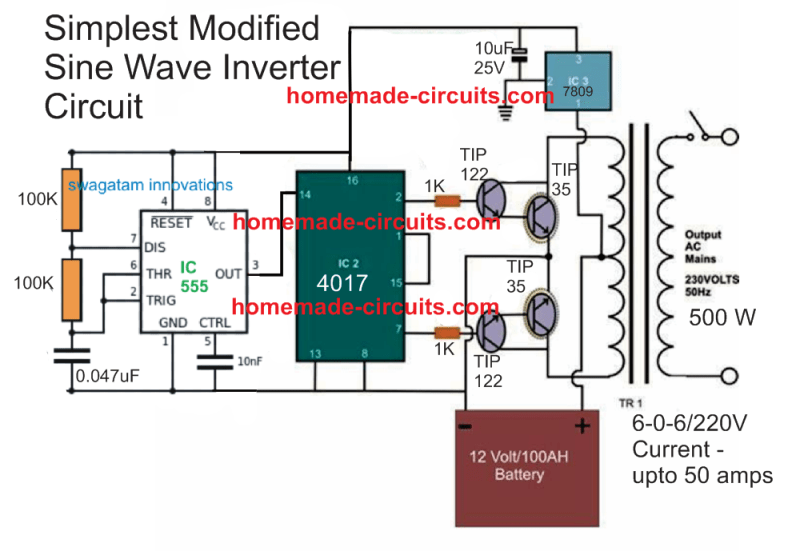
WARNING: PLEASE CONNECT PROTECTION DIODES ACROSS THE COLLECTOR EMITTER OF THE TIP35 TRANSISTOR (CATHODE TO COLLECTOR, ANODE TO EMITTER)
UPDATE: As per the Calculations presented in the this article, the IC 4017 output pins could be ideally configured for achieving an impressive looking modified sinewave inverter.
The modified image can be witnessed below:
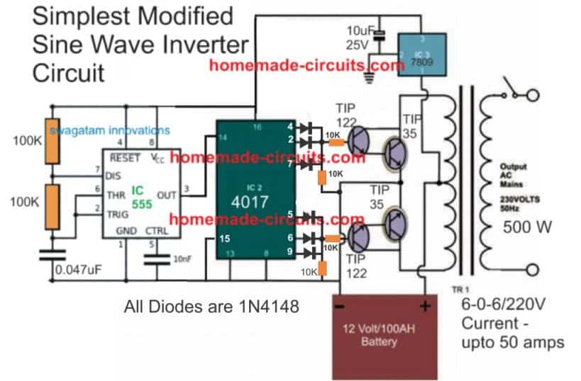
WARNING: PLEASE CONNECT PROTECTION DIODES ACROSS THE COLLECTOR EMITTER OF THE TIP35 TRANSISTOR (CATHODE TO COLLECTOR, ANODE TO EMITTER)
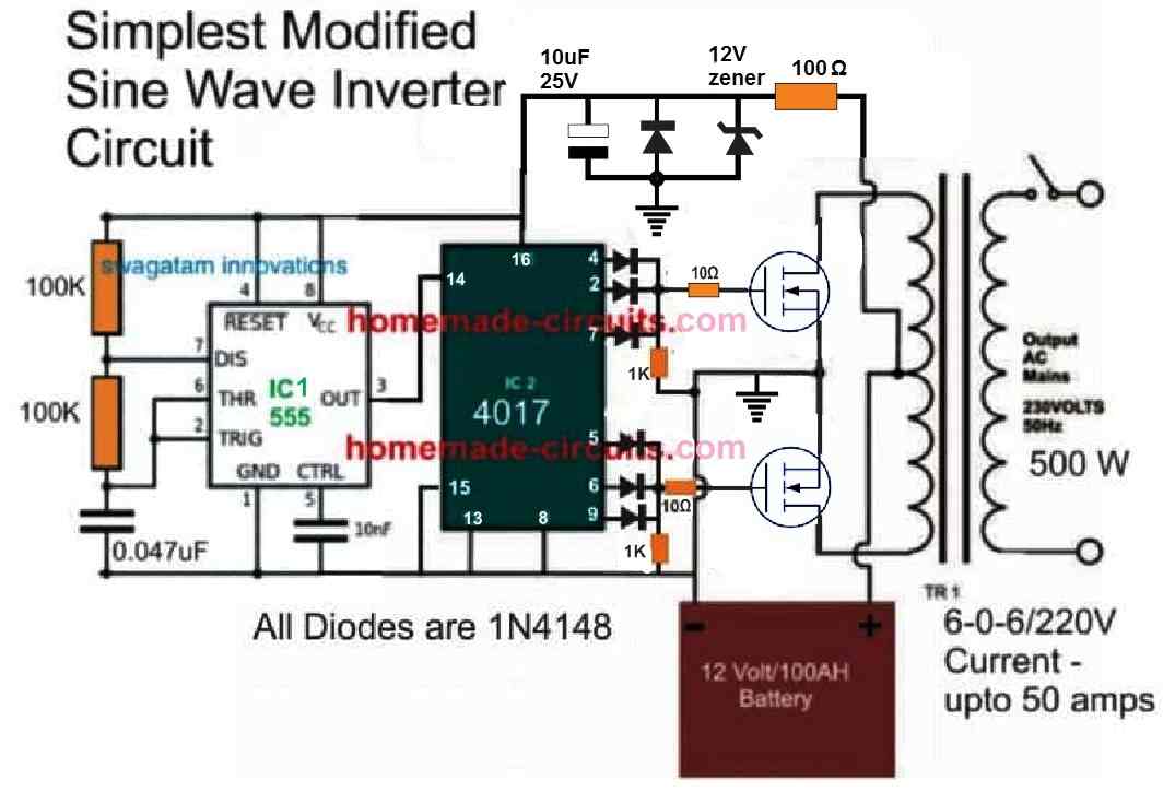
A MOSFET version of the above design can be witnessed in the following diagram. Using MOSFETs IRF3205 can allow the inverter to handle above 400 watts.
Video Demo:
Minimum Specifications
- Input: 12V from Lead Acid Battery, for example 12V 7Ah battery
- Output: 220V or 120V depending on transformer rating
- Waveform : Modified sinewave
Feedback from one of the dedicated viewers of this blog, Ms Sarah
Hello Swagatam,
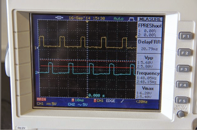
This is what I obtained from the output of IC2 post resistors R4 and R5. As I earlier said I expected to have a bipolar wave. One in positive and the other in negative . to simulate an ac wave cycle. I hope this picture will help. I need a way forward please.
Thanks
My Reply:
Hello Sarah,
The IC outputs will not show bipolar waves since the signals from these outputs are intended for identical N type transistors and from a single supply....it's the transformer which is responsible for creating the bipolar wave at its output since it's configured with a push-pull topology using a center tap ....so what you are seeing across R4 and R5 are correct waveform. Please check the waveform at the output of the transformer for verifying the bipolar nature of the waveform.
Design#2: Using NOT Gates
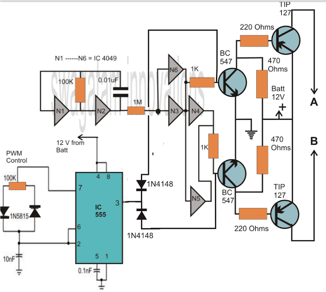
This second in the list is a unique modified sine wave inverter concept also designed me. The entire unit along with the oscillator stage and the output stage can be easily built by any electronic enthusiast at home. The present designed will be easily able to support 500 VA of output load.
Let's try to understand the circuit functioning in details:
The Oscillator Stage:
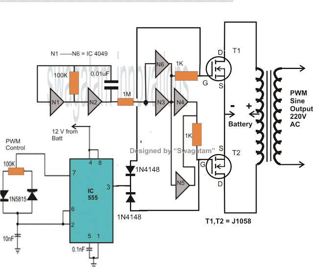
Looking at the circuit diagram above, we see a clever circuit design comprising both, the oscillator as well as the PWM optimization feature included.
Here, the gates N1 and N2 are wired up as an oscillator, which primarily generates perfectly uniform square wave pulses at its output. The frequency is set by adjusting values of the associated 100K and the 0.01 uF capacitor. In this design it is fixed at the rate of around 50 Hz. The values can be altered appropriately for getting a 60 Hz output.
The output from the oscillator is fed to the buffer stage consisting of four parallel and alternately arranged NOT gates. The buffers are used for sustaining perfect pulses and for avoiding degradation.
The output from the buffer is applied to the driver stages, where the two high-power darlington transistors take the responsibility of amplifying the received pulses, so that it can be finally fed to the output stage of this 500 VA inverter design.
Until this point the frequency is just an ordinary square wave. However the introduction of the IC 555 stage entirely changes the scenario.
The IC 555 and its associated components are configured as a simple PWM generator. The mark-space ratio of the PWM can be discretely adjusted with the help of the pot 100K.
The PWM output is integrated to the output of the oscillator stage via a diode. This arrangement makes sure that the generated square wave pulses are broken into pieces or chopped as per the setting of the PWM pulses.
This helps in reducing the total RMS value of the square wave pulses and optimize them as close as possible to a sine wave RMS value.
The pulses generated at the bases of the driver transistors are thus perfectly modified to resemble sine wave forms technically.
The Output Stage:
The output stage is quite straight forward in its design. The two winding of the transformer are configured to the two individual channels, consisting of banks of power transistors.
The power transistors at both the limbs are arranged in parallel to increase the overall current through the winding so as to produce the desired 500 watts of power.
However to restrict thermal runaway situations with the parallel connections, the transistors are connected with a low value, high wattage wire wound resistor at their emitters. This inhibits any single transistor from getting over loaded and fall into the above situation.
The bases of the assembly are integrated to the driver stage discussed in the previous section.
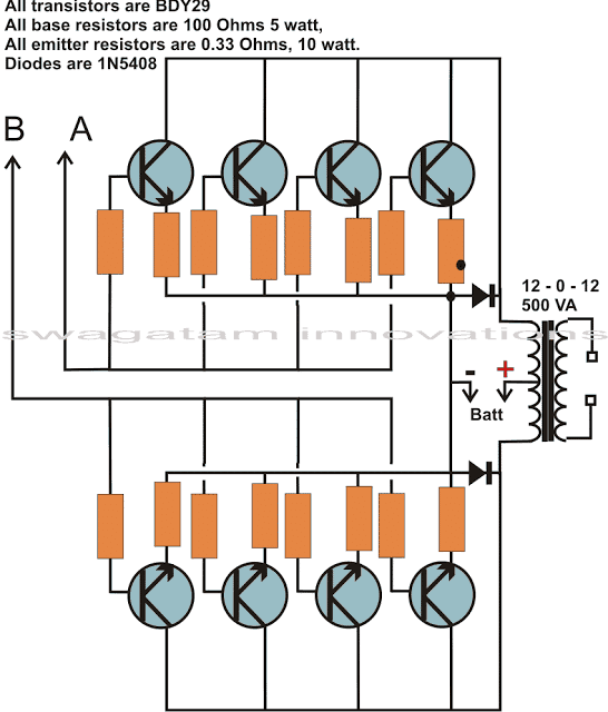
The battery is connected across the center tap and the ground of the transformer and also to the relevant points in the circuit.
Switching ON power immediately starts the inverter, providing rich modified sine wave AC at its output, ready to be used with any load upto 500 VA.
The component details are supplied in the diagram itself.
The above design can also be modified into a 500 watt PWM controlled mosfet sine wave inverter by replacing the driver transistors simply by a few mosfets. The design shown below would provide about 150 watts of power, for obtaining 500 watts, more number of mosfets may be required to be connected in parallel with the existing two mosfets.
Design#3: using a 4093 IC for the Modified Results
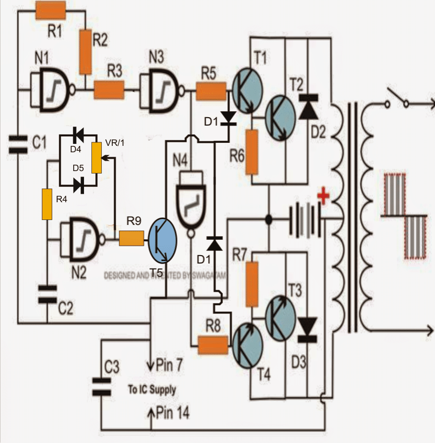
The PWM controlled modified sine wave inverter circuit presented below is our 3rd contender, it uses just a single 4093 for the specified functions.
The IC consists of four NAND gates, out of which two are wired up as oscillators while the remaining two as buffers.
The oscillators are integrated in such a way that the high frequency from one of the oscillators interacts with the output of the other, generating chopped square waves whose RMS value can be well optimized to match the regular sine waveforms.Inverter designs are not always easy to understand or build, especially so when it's as complex as modified sine wave types. However the concept discussed here utilizes just a single IC 4093 for handling all the required complications. I have explained how simple it is to build.
Parts you will Ned to Build this 200 Watt Inverter Circuit
All Resistors are 1/4 watt, 5 %, unless otherwise specified.
- R1 = 1 M for 50 Hz and 830 K for 60 Hz
- R2 = 1 K,
- R3 = 1 M,
- R4 = 1 K,
- R5, R8, R9 = 470 Ohms,
- R6, R7 = 100 Ohms, 5 Watt,
- VR 1 = 100 K,
- C1, C2 = 0.022 uF, Ceramic Disc,
- C3 = 0.1, disc ceramic
- T1, T4 = TIP 122
- T3, T2 = BDY 29,
- N1, N2, N3, N4 = IC 4093,
- D1, D1, D4, D5 = 1N4007,
- D3, D2 = 1N5408,
- Transformer = 12 -0 – 12 volts, current from 2 to 20 Amps as desired, output voltage can be 120 or 230 volts as per country specifications.
- Battery = 12 volts, typically a 32 AH type, as used in cars is recommended.
Circuit Operation
The proposed design of a 200 watt modified sine wave inverter obtains its modified output by discretely “cutting” the basic square wave pulses into smaller sections of rectangular pulses. The function resembles to a PWM control, commonly associated with IC 555.
However, here the duty cycles cannot be varied separately and is kept equal throughout the available variation range. The limitation does not affect the PWM function by much, since here we are only concerned in keeping the RMS value of the output close to its sine wave counter, which is executed satisfactory through the existing configuration.
Referring to the circuit diagram, we can see that the entire electronics hovers around a single active part – the IC 4093.
It consists of four individual NAND Schmitt gates, all of them have been engaged for the required functions.
N1 along with R1, R2 and C1 forms a classic CMOS Schmitt trgger type of oscillator where the gate is typically configured as an inverter or a NOT gate.
The pulses generated from this oscillator stage are square waves which forms the basic driving pulses of the circuit. N3 and N4 are wired up as buffers and are used for driving the output devices in tandem.
However these are ordinary square wave pulses and do not constitute the modified version of the system.
We can easily use the above pulses solely for driving our inverter, but the result would be an ordinary square wave inverter, not suitable for operating sophisticated electronic gadgets.
The reason behind this is that, square waves may differ greatly from the sine waveforms, especially as far as their RMS values are concerned.
Therefore, the idea is to modify the generated square waveforms so that its RMS value closely matches with a sine waveform. To do this we need to dimension the individual square waveforms through some external intervention.
The section comprising N2, along with the other associated parts C2, R4 and VR1, forms another similar oscillator like N1. However this oscillator produces higher frequencies which are tall rectangular shaped.
The rectangular output from N2 is fed to the basic input source of N3. The positive trains of pulses have no effect on the source input pulses due to the presence of D1 which blocks the positive outputs from N2.
However, the negative pulses are allowed by D1 and these effectively sink the relevant sections of the basic source frequency, creating kind of rectangular notches in them at regular intervals depending upon the frequency of the oscillator set by VR1.
These notches or rather the rectangular pulses from N2 can be optimized as desired by adjusting VR1.
The above operation cuts the basic square wave from N1 into discrete narrow sections, lowering the average RMS of the waveforms. It is advised that the setting is done with the help of a RMS meter.
The output devices switch the relevant transformer windings in response to these dimensioned pulses and produce corresponding high voltage switched waveforms at the output winding.
The result is a voltage which is quite equivalent to a sine wave quality and is safe for operating all types of household electrical equipment.
The inverter power may be increased from 200 watts to 500 watts or as desired simply by adding more numbers of T1, T2, R5, R6 and T3, T4, R7, R8 in parallel over the relevant points.
Salient Features of the Inverter
The circuit is truly efficient and moreover it is a modified sine wave version which makes it outstanding in its own respect.
The circuit utilizes very ordinary, easy to procure types of components and is also very cheap to build.
The modifying process of the square waves into sine waves can be done by varying a single potentiometer or rather a preset, which makes the operations pretty simple.
The concept is very basic yet offers high power outputs which may be optimized as per ones own needs just by adding a few more number of output devices in parallel and by replacing the battery and the transformer with the relevant sizes.
Design#4: Fully Transistor Based Modified Sinewave
A very interesting circuit of a modified sine wave inverter is discussed in this article which incorporates just ordinary transistors for the proposed implementations.
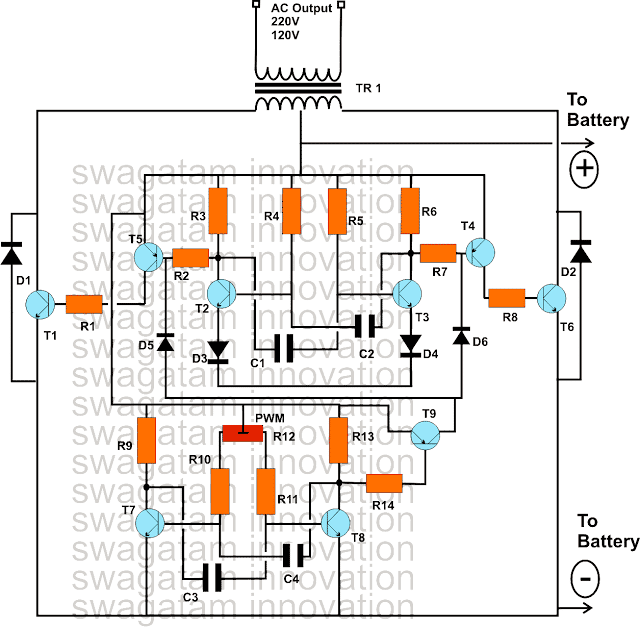
The use of transistors typically makes the circuit easier to understand and more friendly with the new electronic enthusiasts. The inclusion of a PWM control in the circuit makes the design very efficient and desirable as far as operations of sophisticated appliances are concerned at the inverter output.The circuit diagram shows how the entire circuit is laid down. We can clearly see that only transistors have been involved and yet the circuit can be made to produce well-dimensioned PWM controlled waveform for generating the required modified sinew waveforms or rather modified square waves to be more precise.
The whole concept may be understood by studying the circuit with the help of the following points:
Astable as the Oscillators
Basically we can witness two identical stages which are wired up in the standard astable multivibrator configuration.
Being astable in nature the configurations are specifically intended for generating free running pulses or square wave at their respective outputs.
However the upper AMV stage is positioned for generating the normal 50 Hz (or 60 Hz) square waves which are used for operating the transformer and for the required inverter actions, in order to get the desired AC mains power at the output.
Therefore there’s nothing too serious or interesting about the upper stage, typically it consists a central AMV stage consisting of T2, T3, next comes the driver stage consisting of the transistors T4, T5 and finally the receiving output stages consisting of the T1 and T6.
How the Output Stage Works
The output stage drives the transformer via the battery power for the desired inverter actions.
The above stage is only responsible for carrying out the generation of the square wave pulses that’s imperatively required for the intended normal inverting actions.
The PWM Chopper AMV Stage
The circuit at the lower half is the section which actually does the sine wave modifications by switching the upper AMV according to its PWM settings.
Precisely, the upper AMV stage’s pulse shape is controlled by the lower AMV circuit and it implements the square wave modification by chopping the basic square inverter square waves from the upper AMV into discrete sections.
The above chopping or dimensioning is executed and defined by the setting of the preset R12.
R12 is used for adjusting the mark space ratio of the pulses generated by the lower AMV.
According to these PWM pulses, the basic square wave from the upper AMV is chopped into sections and the average RMS value of the generated waveform is optimized as close as possible to a standard sine waveform.
The remaining explanation regarding the circuit is pretty ordinary and may be done by following the standard practice that’s normally employed while building invertes, or for that matter, my other related article may be referred for acquiring the relevant information.
Parts List
- R1, R8 = 15 Ohms, 10 WATTS,
- R2, R7 = 330 OHMS, 1 WATT,
- R3, R6, R9, R13, R14 = 470 OHMS ½ WATTS,
- R4, R5 = 39K
- R10, R11 = 10K,
- R12 = 10K PRESET,
- C1-----C4 = 0.33Uf,
- D1, D2 =1N5402,
- D3, D4 = 1N40007
- T2, T3, T7, T8= 8050,
- T9 = 8550
- T5, T4 = TIP 127
- T1, T6 = BDY29
- TRANSFORMER = 12-0-12V, 20 AMP.
- T1, T6, T5, T4 SHOULD BE MOUNTED OVER SUITABLE HEATSINK.
- BATTERY = 12V, 30AH
Design#5: Digital Modified Inverter Circuit
This 5th design of a classic modified inverter is yet another design developed by me, although it's a modified sine wave, it can also be referred as a digital sine wave inverter circuit.
The concept is again inspired from a mosfet based powerful audio amplifier design.
Looking at the main power amp design we can see that basically it's a 250 watt powerful audio amp, modified for an inverter application.
All the stages involved are actually for enabling a frequency response of 20 to 100kHz, though here we won't need such high degree of frequency response, I didn't eliminate any of the stages as it wouldn't do any harm to the circuit.
The first stage consisting of the BC556 transistors is the differential amplifier stage, next comes the well balanced driver stage consisting of the BD140/BD139 transistors and finally it's the output stage which is made up of the powerful mosfets.
The output from the mosfets are connected to a power transformer for the required inverter operations.
This completes the power amp stage, however this stage requires a well dimensioned input, rather a PWM input which would ultimately help to create the proposed digital sine wave inverter circuit design.
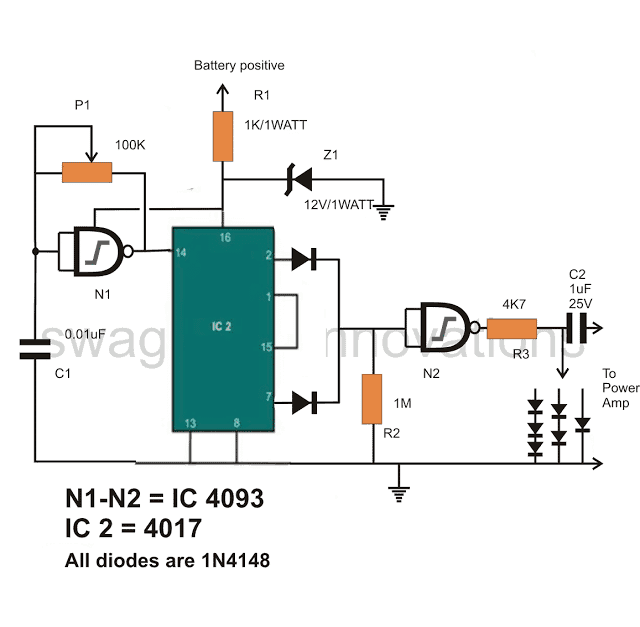
The Oscillator Stage
The next CIRCUIT DIAGRAM shows a simple oscillator stage which has been suitable optimized for providing adjustable PWM controlled outputs.
The IC 4017 becomes the main part of the circuit and generates square waves which very closely matches the RMS value of a standard AC signal.
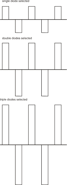
However for precise adjustments, the output from the IC 4017 has been provided with discrete voltage adjustment level facility using a a few 1N4148 diodes.
One of the diodes at the output may be selected for reducing the amplitude of the output signal which would ultimately help in adjusting the RMS level of the transformer output.
The clock frequency which must be adjusted to 50Hz or 60Hz as per the requirements is generated by a single gate from the IC 4093.
P1 can be set for producing the above required frequency.
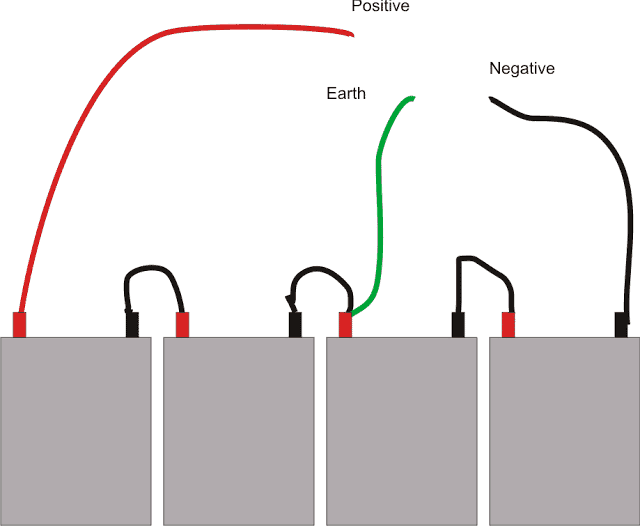
For getting a 48-0-48volts, use 4 nos. 24V/2AH batteries in series, as shown in the last figure.
Power Inverter Circuit
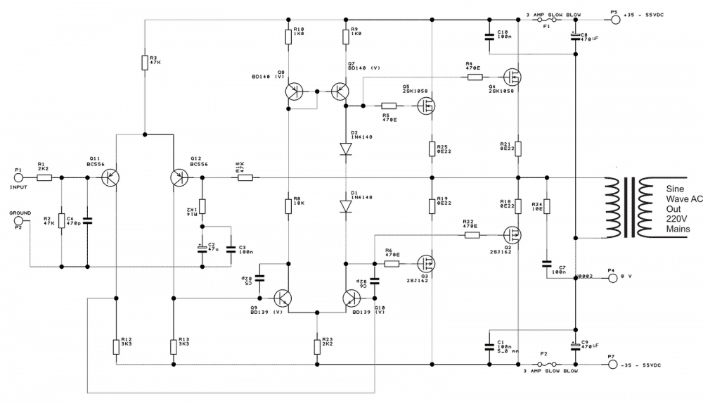
Sine Wave Equivalent Oscillator Circuit
The figure below shows various waveforms outputs as per the selection of the number of diodes at the output of the oscillator stage, the waveforms may have different relevant RMS values, which must be carefully selected for feding the power inverter circuit.
If you have any problems understanding the above circuits, please feel free to comment and inquire.
Design#6: using only 3 IC 555
The following section discusses the 6th best modified sine wave inverter circuit with waveform images, confirming the credibility of the design. The concept was designed by me, the waveform being confirmed and submitted by Mr. Robin Peter.
The discussed concept was designed and presented in a few of my previously published posts: 300 watt sine wave inverter circuit, and 556 inverter circuit however since the waveform were not confirmed by me the relevant circuits weren't completely foolproof.Now it's been tested, and waveform verified by Mr. Robin Peter, the procedure revealed one hidden flaw in the design which has been hopefully sorted out here.
Let's go through the following email conversation between me and Mr. Robin Peter.
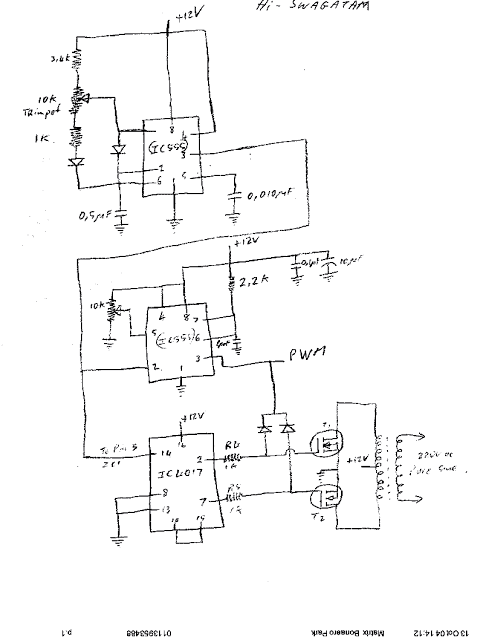
I built the simpler modified sine wave alternative version IC555's,with no transistor. I changed some of the values of the resistors and caps and did not use[D1 2v7,BC557,R3 470ohm]
I joined Pin2&7 of IC 4017 together to get the required waveform. IC1 produces the 200hz 90% duty cycle pulses(1 image), which clock IC2 (2-images) and therefore IC3(2 images, min duty cycle & max D/C)Are these the expected results, My concern is that it is a modified sine where you can vary the
RMS,not a pure sine
Regards
Robin
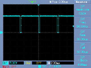
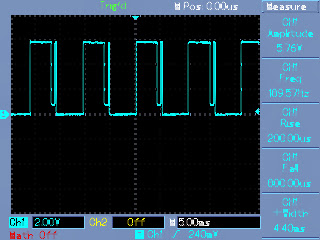
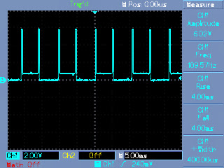
Hi Robin,
Your modified sine wave circuit diagram looks correct but the waveform isn't, I think we'll need to use a separate oscillator stage for clocking the 4017 with frequency fixed at 200Hz, and increase the frequency of the topmost 555 IC to many kHz, then check the waveform.Regards.
Hi Swagatam
I have attached a new circuit schematic with the changes you suggested along with the resultant wave forms.What do you think of the PWM waveform,the pulses don't seem to go all the way down to ground
level.
Regards
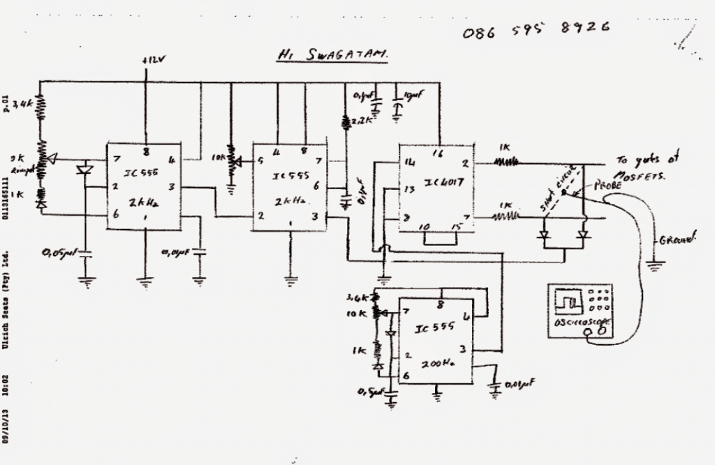
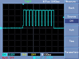
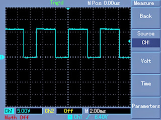
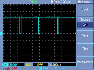
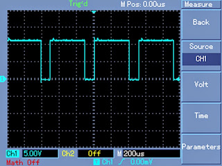
Hi Robin,
That's great, exactly what i was expecting, so it means a separate astable for the middle IC 555 must be employed for the intended results....by the way did you vary the RMS preset and check the waveforms, please do update by doing so.
So now it looks much better and you can go ahead with the inverter design by connecting the mosfets.
....it's not reaching the ground due to the diode 0.6V drop, I assume....Thanks very much
Actually a much easier circuit with similar results as above can be built as discussed in this post:https://www.homemade-circuits.com/2013/04/how-to-modify-square-wave-inverter-into.html
More Updates from Mr. Robin
Hi Swagatam
I varied the RMS preset and here are the attached waveforms.I would like to ask you what amplitude of triangle wave can you apply to pin 5,and how would you synchronise it so that when pin 2 or 7 go + the peak is in the middle
regards Robin
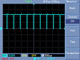
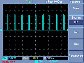
Here's some better modified sine waveform, maybe the guy's will understand them easier. It's up to you whether you publish them.
By the way i took a 10uf cap from pin2 to 10k resistor to .47uf cap to ground.And the triangular wave looked like this(attatched).Not too triangular,7v p-p.
I will investigate the 4047 option
cheers Robin
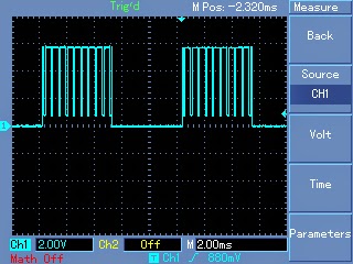
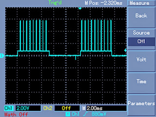
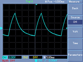
Output Waveform across Transformer Mains Output (220V)The following images show the various waveform images taken from across the output mains winding of the transformer.
Courtesy - Robin Peter
No PWM, no Load
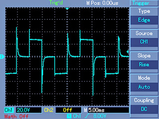
No PWM, with load
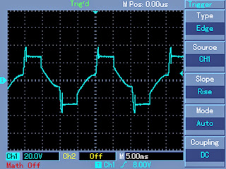
With PWM, without load
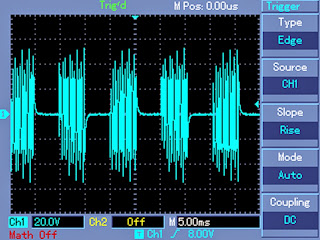
With PWM, with load
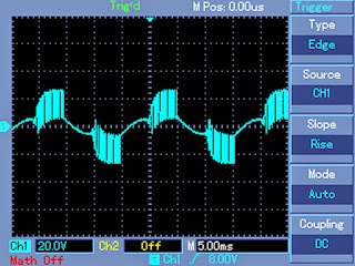
The above image magnified
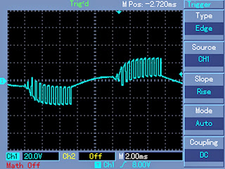
The above waveform images looked somewhat distorted and not quite like sinewaves. Adding a 0.45uF/400V capacitor across the output drastically improved the results, as can be witnessed from the following images.
Without load, with PWM ON, capacitor 0.45uF/400v added
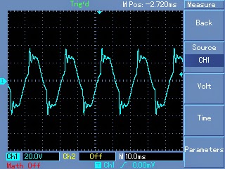
With PWM, with load, and with an output capacitor, this looks very much like an authentic sinewaveform.
All the above verification and testing were conducted by Mr. Robin Peters.
More Reports from Mr. Robin
Ok,I did some more testing and experimenting last night and found that if I increase the batt voltage to 24v the sinewave did not distort when I increased the duty/cycle.( ok,I've regained my confidence)I added that 2200uf cap between c/tapp and ground but that made no difference to the output waveform.
I noticed a few things that were taking place,as I increased the D/C the trafo makes a noisy humming sound(as if a relay is vibrating back and forth very quickly),The IRFZ44N's get hot very quickly even with no loadWhen I remove the cap there seems to be less stress on the system.The humming noise is not so bad and the Z44n's don't get so hot.[of course no sinewave}
The cap is across the output of the trafo not in series with one leg. I took (3 different windings) round inductors{I think they are toriodal} out of a switch-mode power supply.The result was no improvement in the output wave(no change),
The trafo output voltage also dropped.
Adding an automatic load correction feature to the above modified sine wave inverter circuit idea:
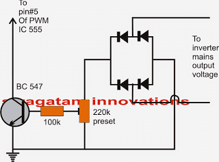
The above shown simple ad-on circuit can be used for enabling automatic voltage correction of the inverter output.
The fed voltage across the bridge is rectified and applied to the base of the NPN transistor. The preset is adjusted such that at no load the output voltage gets settled at the specified normal level.
To be more precise, initially the above preset should be kept at the ground level so that the transistor says switched OFF.
Next, the 10k RMS preset at pin#5 of the PWM 555 IC should be adjusted to generate around 300V at the transformer output.
Finally, the load correction 220K preset should be realigned to bring down the voltage to may be around 230V mark.
Done! Hopefully the above adjustments would be enough for setting up the circuit for the intended automatic load corrections.
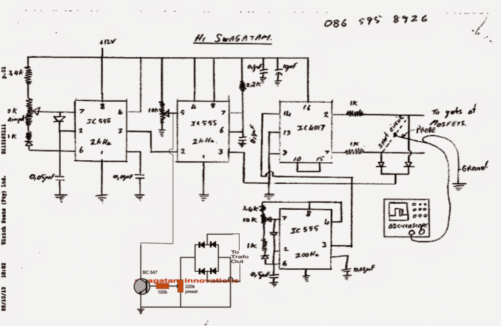
The final design might look like this:
Filter Circuit
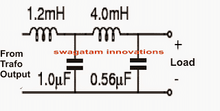
The following filter circuit can be employed at the output of the above inveter for controlling Harmonics and for enhancing a cleaner sinewave output
More Inputs:
The above design was studied and further improved by Mr Theofanakis, who is also an avid reader of this blog.
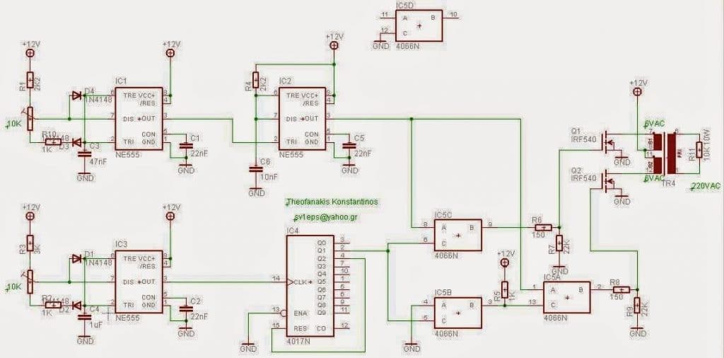
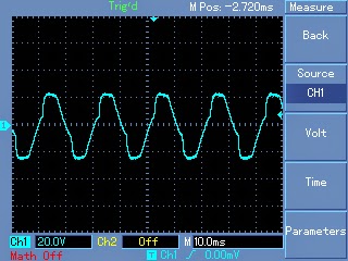
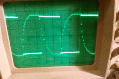
The oscilloscope trace depicts the modified waveform of the inverter across the 10k resistor connected at the mains output of the transformer.
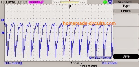
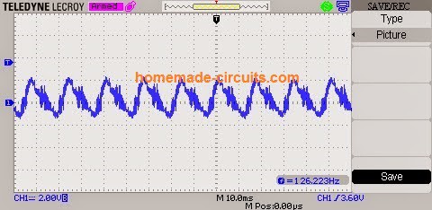
The above modified inverter design by Theofanakis inverter was tested and approved by one of the avid followers of this blog, Mr. Odon. The following test images by Odon confirm the sinewave nature of the above inverter circuit.
Design#7: Heavy Duty 3Kva Modified Inverter Design
The below explained content investigates a 3kva sine wave inverter circuit prototype made by Mr. Marcelin using only BJTs instead of the conventional mosfets. The PWM control circuit was designed by me.
In one of my previous posts I have explained a 555 pure sine wave equivalent inverter circuit, which was collectively designed by Mr.Marcelin and me.
How the Circuit was Built
In this design I have used strong cables to sustain the high currents, I used sections of 70 mm2, or more smaller sections in parallel. 3 KVA transformer is actually as solid weighs 35 kg. Dimensions and volume is not a drawback for me. Photos attached to the transformer and installation in progress.
The following assembly nearing completion, based on the 555 (SA 555) and CD 4017
On my first try, with mosfets, earlier this year, I used IRL 1404 which Vdss is 40 volts. In my opinion insufficient voltage. It would be better to use mosfets with a Vdss at least equal to or greater than 250 volts.
In this new installation, I foresee two diodes on the transformer windings.
There will also be a fan for cooling.
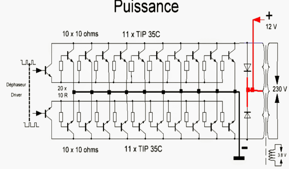
TIP 35 will be mounted by 10 in each branch, like this:
Complete Prototype Images
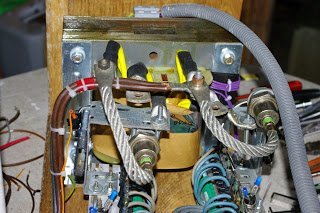
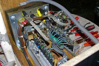
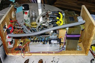
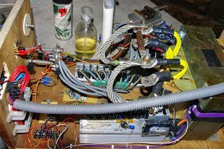
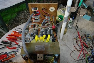
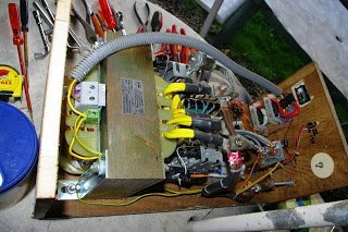
Finalized 3 KVA Inverter Circuit
The final circuit design of the 3 kva modified sine wave inverter should look like this:
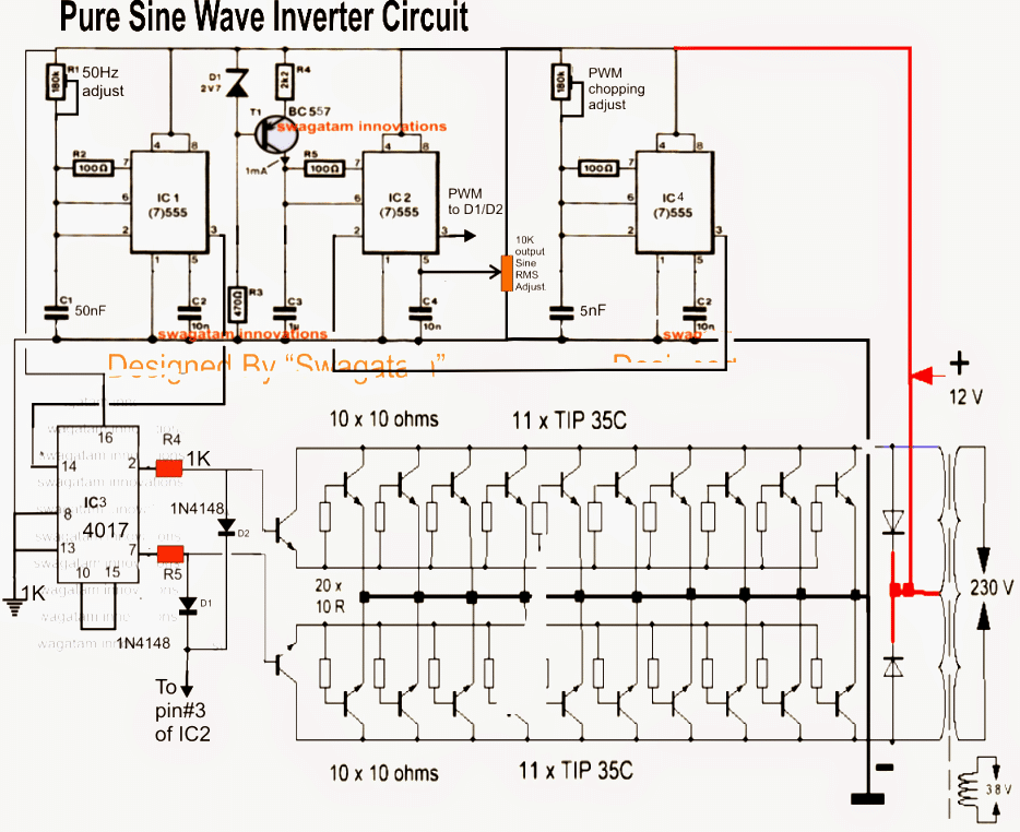
Parts List
All resistors are 1/4 watt 5%, unless specified.
- 100 Ohms - 2nos (value can be between 100 ohm and 1K)
- 1K - 2nos
- 470 ohms - 1no (can be any value upto 1K)
- 2K2 - 1nos (slightly higher value will also work)
- 180K preset - 2nos (any value between 200K and 330K will work)
- 10K preset - 1no (please 1k preset instead for better outcome)
- 10 Ohm 5 watt - 29nos
Capacitors
- 10nF - 2nos
- 5nF - 1no
- 50nF - 1no
- 1uF/25V - 1no
Semiconductors
- 2.7V zener diode - 1no (upto 4.7V can be used)
- 1N4148 - 2nos
- 6A4 diode - 2nos (near transformer)
- IC NE555 - 3 nos
- IC 4017 - 1no
- TIP142 - 2nos
- TIP35C - 20 nos
- Transformer 9-0-9V 350 amps or 48-0-48V / 60 amps
- Battery 12V / 3000 Ah, or 48V 600 Ah
If 48V supply is used then make sure to regulate it to 12V for the IC stages, and supply the 48V only to center tap of the transformer.
How to Safeguard the Transistors
Note: In order to safeguard the transistors from a thermal runaway, mount the individual channels over common heatsinks, meaning use a long single finned heatsink for the upper transistor array, and another similar single common heatsink for the lower transistor array.
Mica isolation would be fortunately not required since the collectors are joined together, and the body being the collector would get effectively connected through the heatsink itself. This would actually save a lot of hard work.
In order to obtain maximum power efficiency, the following output stage is recommended by me, and must be employed with the above explained PWM and 4017 stages.
Circuit Diagram
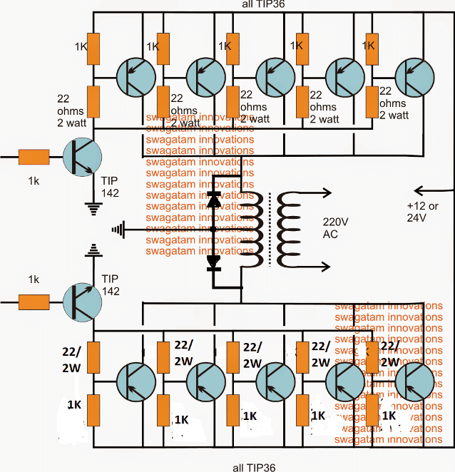
Note: Mount all the upper TIP36 over a larger finned common heatsink, DO NOT use mica isolator while implementing this.
The same must be done with the lower TIP36 arrays.
But make sure these two heatsinks never touch each other.
The TIP142 transistors must be mounted on separate individual large finned hearsinks.

Sir i want to use 24v battery should i use ic7812 for reducing it to 12voltage for the ic circuit
You can use 7812 for the IC circuit. Use an additional 100 ohm resistor in series with the output of the 7812 IC.
Sir please can i connect 1uf 400v capacitor at the output of the transformer
John, you will need 3nos of 1uF/400V in parallel.
can I use 1kva transformer for that first circuit with two irfp2907 in each channel
you can use it!
sir is there any different between irf260 and irf260n
I checked the datasheets of the two, they looked identical to me. So both are one and the same.
Sir please can use irfp2907 in that first diagram
Yes, it can be used on all the first 3 diagrams.
sir please is that first diagram a 50hz inverter
yes it is a 50Hz inverter
sir am getting 2.68 volt at the output pin of CD4017
It is average DC value due to the output frequency, the peak value will be always equal to the battery level….use an oscilloscope to test the peak value.
thanks for your reply but I don’t even have oscilloscope
Without an oscilloscope you cannot verify the waveform and you cannot proceed. You can easily buy a small oscilloscope online and use it.
sir everything is working but the problem is that i connect 1k resistor from gate to source and it burnt my mosfet
Hi John, I am not sure why that is happening. The gate/source 1K is supposed to discharge the mosfet internal capacitance quickly and prevent heating up of the mosfet.
If it is not working for you then you can go without it.
sir please can I connect 1N4814 at gate to source for protection
I have never seen a diode being used across gate/source for any kind of protection, it might not be relevant according to me.
sir connection of 20amp diodes between the center tap wire and the side wire does it help to protect the mosfet
Yes, that helps! It is same as connecting a diode across drain/source of the mosfet.
sir can i use that first diagram to power my freezer and CRT television
Yes you can according to me….
Hello Swagatam, in the first circuits in design 1 above. Can I use a single 100ohms to serve 5 Mosfet’s then the other side also a single 100 ohms or each mosfet should have its 100 ohms at the gate? Which connection is more efficient? Secondly, I want to use 10 Mosfet’s. Should i use blocking diodes across drain and source pins? Thanks in advance!
Hello Morris, The resistor value is actually 10 ohms, not 100 ohms. You can use a common gate resistor for all the MOSFETs, but using individual gate resistors for each MOSFET will be more efficient.
Thanks sir. What about the blocking diode across the drain and source pins of the Mosfets?
The diode can be a single diode across the parallel set of MOSFETs, although these diodes are already installed internally for each of the MOSFETs
Yes sir, at the output of ac now I only got 335j 400v instead of 3uf 400v(ppc). Can this 335j 400v work? Thanks in advance.
Hi Morris, you can try the 335j 400v at the output and see how it responds.
Hello sir, I tried the first design in this circuit but the output am getting is 127. I hv tried two different transformers 9-0-9 but still the same. What could be the problem?
Hi Morris,
Please check the average Dc across gate/source of the MOSFET, this value will indicate the actual required primary voltage of the transformer. For example if this voltage is 6V then the transformer should be 6-0-6V and so on.
Once you do this your output will be a perfect 220V or higher.
So you mean that I first connect the battery then I measure the screen voltage across gate/source of the MOSFETs. Then if i find it reads 8v then i use 8-0-8 transformer to get me an output of around 220v ac or higher?
Yes that will work!
Hello sir, I have thoroughly checked my circuit ten times to see where I did a mistake but it’s exactly as yours here. Whn I measure the voltage across gate/source as u said after connecting the battery without transformer only getting 2.2v and when I changed 4017 and 555 it is 3.4v ???????????? what’s your thought about that? I really wanted this modified sine wave inverter sir
Hello Morris,
please check the voltage across the 1K resistors in the following diagrams:
https://www.homemade-circuits.com/wp-content/uploads/2022/04/modified-inverter-using-mosfets.jpg
Make sure to use a good multimeter.
Let me know the results.
Normally it should be around 50% of the voltage which is available at the positive rail of the ICs.
Hello sir the voltage am seeing at the output of 4017 across the 1k resistor is a sequence voltage running from 1.1v to 3.7v then starts again I hv checked and replaced several IC’s but still the same. The voltages at all the pins of 555 time are constant but at 4017 Pins is a running up and down voltage. Do u hv another efficient one pliz
Hello Morris, The frequency at these pinouts is supposed to be very fast and the DMM should show the average voltage only…so I cannot figure out how the voltage is fluctuating in your case.
Anyway, do you have an analogue voltmeter, please test the same with an analogue voltmeter.
Hello Swagatam.merry Christmas and a happy new year in advance! Pliz can you lecture me on something here. (1) I have four rooms to be supplied with light. What do you prefer in terms of battery safety whn you are using inverter for lighting or whn you’re using dc battery bulbs for lighting? If dc bulbs are good and u know in the four rooms there will be a voltage drop because of the long cables in the conduits (pipes) so do you have a 12v dc to 14 or 15v dc there about for each bulb to get at least 12v dc in the end? (2) if impossible, do u have best suited inverter circuit that will not affect battery life? Am abit confused my friend on which idea will save battery life. Pliz help. Thanks.
Hello Morris,
I think an inverter would be a better option than using DC for lighting LED bulbs with long cables. Since an inverter produces an AC, the length of the wires will have negligible impact on the performance. You can easily use any 4047 IC based square wave inverter to power your LEDs. If you use an inverter you can directly connect an AC 220V LED bulb at the outputs of the inverter.
A simple 4047 inverter circuit is discussed in the following article:
7 Simple Inverter Circuits you can Build at Home
So using a 200w or a 300w inverter will be just ok and will not shorten battery life as others say? But do u have dc-dc booster circuits to around 14v? What I fear with dc light is the drop of the voltage. So if u say inverter is the perfect one then I will just use the ac bulbs for lighting
If you use DC then using long wires might affect the illumination, that is why I suggested using an inverter.
Yes AC bulb will be good which can remain illuminated even if the AC drops to 100 V, which means even if the battery drops to 10 V from 12V still the LED bulbs will remains illuminated, although it is not recommended for a 12V battery to be discharged below 11V.
Why do you need a booster circuit?
I was considering which way can save battery life and which way will shorten battery life. That is why I seek advice from you between inverter and dc bulbs using dc booster to ensure that the 12v reaches the bulbs. Thanks sir for advice.
Since the inverter would e only 75% efficient, so I think connecting the battery directly with the LED would give better results. But I am sure about the impact of the wires resistance, that you will have to find out through a practical testing.
Hello Swagatam, I built another homemade inverter and the output voltage is 300 then whn i plugged in soldering iron it comes to around 240. Do you have any circuit diagram that I can connect to the inverter output to tame its voltage to be a constant 230 or 220v ac? Thanks in advance sir.
Hello Morris, you can try the second design from the following article:
https://www.homemade-circuits.com/load-independentoutput-corrected/
Thanks sir. So the trafo output is the inverter output of the transformer? Secondly, if we have two panels of the mosfets right and left, and the two in4007 connected to the bc transistor. Do I connect the gates of both left and right panels to each of the in4007 as indicated there?
Thanks
You will need to connect a separate diode with each of the mosfet gates and then connect the common cathode ends of the diodes with the BC547 collector. For indication purpose you can replace the 3V zener diode with a 3V RED LED.
Ok sir but can it work with the 24v inverter because mine is a 24v inverter? And how is the connection now?
Thanks.
Hi Morris, The IC 741 must be operated with 12V, so you may have to connect a 7812 IC for stepping down the 24V to 12V for the 741 IC.
Do the setup need a variable power supply before connecting to the transformer output or how is it set? Thanks anyway.
Please ask your question under the following article, I will try to help:
https://www.homemade-circuits.com/load-independentoutput-corrected/
Hellos sir, do I use IN4007 or just 4148 diode as indicated in this voltage auto correction circuit?
Thanks 🙏
Hello Morris, you can use 1N4148, or 1N4007, just make sure your MOSFET gate resistors are at least 100 ohms. And also connect reverse diodes parallel to these gate resistors.
https://www.homemade-circuits.com/wp-content/uploads/2021/09/adding-a-gate-source-resistor-for-preventing-mosfet-burning.jpg
Gate to source resistor is not required.
So the positive side of the diodes to face the gates of the mosfets??
Yes, the anodes of the diodes connect with the gates.
If you look at the symbol of a diode, the side with a bar or arrow point is the side facing the gate?🤣🤣🤣
Thanks
No, the other side without the bar (anode) goes to the gate, and the bar side (cathode) goes to the IC output.
Thank so much my teacher. But after paralleling all resistors with IN4148 do i need also to use a common IN4148 for each side of the set of the mosfets to the oscillator now or the parallel way is just enough?
Thanks
As shown in the following diagram, the “logic Out” refers to the oscillator output from the oscillator IC. You just have to connect the resistor//diode ends in this manner.
https://www.homemade-circuits.com/wp-content/uploads/2021/09/adding-a-gate-source-resistor-for-preventing-mosfet-burning.jpg
Each resistor to be paralleled with a diode and the positive side to face the gate of a mosfet?
Thanks in advance sir.
Yes, that’s right, as shown in the previous diagram…
Hello Swagatam, am sorry for interruption in this different topic. My question is if I have 4pcs of 100ah 12v batteries. Two sets connected in parallel then connect them again in series. That will form 200ah each side. What is the advantage of that compared to when i just buy 2pcs of 200ah 12v batteries. Which is the best direction to go? 4pcs of 100ah or just 2 pcs of 200ah. Thanks sir.
Hello Morris,
According to me, using a 2pcs of 200Ah battery will be more efficient due to uniform charging/discharging and better power sharing characteristics.
So even if am using 4pcs of 150ah the two pieces of 200ah still stands a better position due to one uniform stength?
Thanks.
yes that’s correct…
You mentioned 4pcs of 100Ah in your previous comment, If you use 4nos of 150Ah then its capacity will be more than two 200Ah batts
OK thanks alot sir. Now, I have mains, inverter and a battery charger. Can you refer me to a better automatic changeover system which may act swiftly when mains goes off and when the mains comes back it picks to main line instantly.
Thanks in advance sir.
Hi Morris, you can try the following concept for the relay changeovers.
https://www.homemade-circuits.com/how-to-convert-inverter-to-ups/
Dear Swagatam
Can the outputs of the 4017drive 2 of ir2110 inorder to get a full h bridge configuration? In that case will the output be a pure sine wave?
Hi Richard,
We normally need 4 FETs to create a full bridge configuration. Using 2 FETs will give us a half wave configuration only. However neither can be built using a 4017 IC. Using full bridge configuration will not convert square wave to sine wave.
Hello Swagatam,
Thank you for your answer. In fact I have tried to modified the speed of the motor (describe 11/5/2022) with a positive (0 to +10 V) square wave to 30 to 1700 Hz through a transistor IRF730 and also a triac BT139 but the speed stays very very low (the motor stays always fed with the sine wave of 50 Hz from the net); that ‘s why I thought to use a sine wave (+ V to – V) to inject directly in the motor in thinking to your circuit in changing the frequency.
Best regards,
Hello Serge,
The modified inverter circuit cannot be used to control the speed of the motor. If your motor is a DC motor then you can try the following concept to control its speed:
3 Simple DC Motor Speed Controller Circuits Explained
thanks for ur educating us sir more longer life
My pleasure Moore!
Dear sir,
With the simplest modified sine wave inverter circuit, is it possible to modified the speed of an electric motor asynchronous 220 V AC 50 Hz 1 phase 50 W on which a 0.2 micro farad capacitor is connected (impossibility to remove it) or I must use a square wave to change the speed?
Best regards,
Hello Serge,
I can’t figure out how the simplest modified inverter can be used to modify the speed of your motor? But it can used to operate your motor normally even with the capacitor connected to the motor. The speed can be controlled either through a PWM system or a triac based speed controller.
hi sir swagatam my diy mod sinewave works fine but how can i remove transormer humming noise and harmonic noise when i power my amplifier with it?
Hi Kenbion,
If you have large filter capacitors with the bridge rectifier and still the hum sound is not going then you may have to attach a hum filter circuit at the input of the amplifier as explained in the following article. Also make sure to connect the ground line of the amplifier with the metal cabinet of the amplifier.
https://www.homemade-circuits.com/simple-hum-filter-circuit-for-amplifiers/
thanks,,but how can i make my inverter run quietly without noise,,,thats what i mean
You can try adding a 3uF/400V capacitor at the output of the inverter and check whether that helps or not.
Sir I have ferrite core transformer also have CD 4017 and timer 555 so which MOSFET use to make simple watt inverter
Hi Abdulkareem, You can use IRF540.
Please give me your WhatsApp number I talk to you
You can discuss with me here, through comments.
Like to have the PCB details for the pure sine wave inverter.
Your doing a good job keep it up thanks,
my inverter power mosfet blow up, it rated 60v 190a and I subtitude it with 60v 50a mosfet and it blows again what’s could cause it?
There can be many reasons, for example a malfunctioning oscillator, or a short circuit on the drain side of the mosfet, or the mosfet itself might be faulty. It will need to be checked with a multimeter to find the exact fault.
Hello Mr Swagatam.
I have a MODIFIED SINE WAVE INVERTER that has stopped working and is 3 months old, out of warranty.
When you turn it on, it lights up the red over voltage LED.
I checked all the MOSFETs and IGBTs and they are ALL good.
The INVERTER brand is GILGAL 4000W peak and 2000W real of the same brand as the KNUP INVERTER.
I reverse engineered it to try to understand how it works, to find the DEFECT.
But it’s very difficult because it’s a dual board and the components hide the tracks.
But still, I managed to lift the Circuit.
It has a DRIVER with 4 MOSFETs in the first stage, DC voltage riser.
And a DRIVER with 4 IGBT in the second stage of CA.
And a PWM BOARD.
But, I don’t understand, because he also has 2 MOSFET to provide the NEGATIVE side of the BATTERY, for the DRIVER.
Thanks.
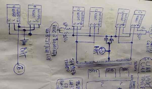
Hi Paulo,
The 4 mosfets and the center tap inverter transformer appears to be a standard inverter configuration, but even I cannot figure out why those two extra mosfets on the left side are provided?
I can see the drains of those 2 mosfets are connected with the ground symbol, so I am not sure what this ground symbol indicates?
Even I find it difficult to understand this schematic.
sir which mosfet is make
You can IRF540 or IRF3205, or IRF2907
ferrite trans to covert 200inveter circuit
You will have to calculate it, I don’t have the ready made example.
That’s it, thanks. I believe that if I follow all your instructions and video I will produce the 1k watts design with sinewave. Also through adding calculated capacitors at the output, sinewave is assured even without a scope around. I heard that there’s a software that can be used on the PC to check waveform and frequency of a.c. and other things
OK great! However for sinewave you will have to try the second schematic which has diodes connected across the 4017 output, the first diagram will produce crude modified only, whereas the second schematic will produce improved modified sine wave, or even pure sine wave.
I am not very sure about the software, you may have to search for it online.
Thank you sir very much sir for your advice. I have built a simple inverter before using only two mosfets, and it’s working very fine, no glitching or shaking but it’s square wave, not good for some of our equipments, that’s why I decided to go with the one in the article. Also is there anything like an alternative to oscilloscope, something that can substitute it as regards checking the waveform and output frequency. Getting one now is too costly, there’s huge inflation in my country as regards price of things
No problem Anthony, then you can go ahead with this modified design as discussed in the previous comments. Feedback link can be tested after you have checked the modified design output response.
Without oscilloscope it is not possible to check the waveform, whether it is square wave or modified square wave. You can only check the frequency with a multi-meter but waveform cannot be confirmed without an oscilloscope.
Thanks very much sir for this info ????, pls I do not have a freq. or hz meter or scope ????, is there any alternative that can help me to check frequency and even sine wave pattern output.
Again, sir pls for clarification, IF am to use 8 mosfets for example, you know am going to divide the mosfets into two “SETS” or “SIDES” i.e four on each set and side. So pls are you saying that I should connect only ONE 10- 100 ohms for each side or set of the mosfets gates making it total two.
Also pls do mean that I should connect Only ONE 1k Resistor each to the mosfets gate and source of each side or set,
sir pls if you can draw a circuit for the Resistor connection you explained in the above comment so that I can understand better. Thanks
Then sir pls should we connect the diodes in bridge format and should it go directly to the load. Sir there’s also a diagram of this same inverter we are discussing on now i.e under the first modified sine wave inverter circuits in this article I saw in another comment section where you included the feedback mechanism on it using BC557 transistor, 10k resistor, BC547 transistor, 1k preset, 1m Resistor and 5 1N4148 diodes, should I use exactly these components in the manner that you connected them in the diagram for the 1k watt design. Pls sir a diagram of it will help me to understand better thanks.
Hello Anthony, when you connect the mosfets in parallel you get one common gate, a common drain, and a common source for both the channels.
Connect the gate resistor between the common gate and the 4017 output, and connect the 1K between common gate and common source.
I think you should first build a single mosfet inverter and test its working
Without a small oscilloscope and digital multimeter you cannot build an inverter, and helping you might also be difficult.
If you connect a bridge at the output it will produce DC not AC to the load.
Please do not consider feedback at this moment, build the basic inverter first for confirmation using an oscilloscope, and then proceed with the next steps..
Happy New Year sir, may the year grant you increase all round for being good ✨. Sir I want to ask under the first modified sine wave circuit, you said that to increase it to 1k Watts I have to replace TIP122 AND TIP35 with few parallel mosfets, sir pls which mosfets should we use, again apart from the mosfets are we to add another set of transistors to the mosfets, then pls when connecting the mosfets should we follow the TIP122 AND TIP35 BCE as in the circuit and connect directly to the mosfet’s GDS or will it be any way combination.
Then sir, you said I should use 6-0-6 transformer to get 240v, is it a must that I must use it to produce 240v, if I use 12-0-12 transformer, how many volts will I produce. Again if you recommend that I can replace the 6-0-6 transf. with 12-0-12 transf . hope it won’t affect the inverter circuit. Thanks
Wish you too a Happy New Year Anthony, You can use IRF3205 mosfets. You can connect all the parallel gates to the 4017 output, drains to the transformer, and sources to the battery negative.
The transformer primary side voltage value should be equal to the DC generated across outputs of the 4017 IC. So please check the voltage between the 4017 output and the ground line, and then you can decide the transformer accordingly.
Thank you very much sir for responding, pls I want to be sure, since am going to connect the mosfets’ gates to pin 2 and 7 of the 4017 IC, for me to test the output DC of the 4017 IC, I guess I have to connect one of the terminals of the digital meter to either pin 2 or 7 of the 4017 IC and the other meter terminal to the battery negative inorder to confirm the voltage I will use to produce the transformer. Am I right pls, thanks.
Hello Anthony, that’s correct!
Make sure to adjust the 555 frequency so that you get 50 Hz on either of the pinouts of 4017, with respect to ground or the negative terminal. And also use resistor between 10 ohm and 100 ohm for the mosfet gate resistor, only one is required for each parallel mosfet channel. Also connect a 1K resistor between the gate/source of the parallel mosfet, again use only one resistor for each of the parallel combination.
Also do not forget to connect diodes between the center tap and the outer wires of the transformers, a 1N5408 will do.
Hello @ swagatam,thanks for your circuits and work, they are all good, pls I want to ask you based on this post’s first article ” Design 1#- using ic 4017″.
First I want to construct and improve it up to 1000watts for some of my home appliances, can I go on with the improvement using the circuit diagram you posted on it. Is it safe for the appliances.
2. Pls in the video you made on it, you used two Transistors ( tip35 and 8050) connected in Darlington mode instead of 4 Transistors according to the circuit diagram. You said we can use MOSFETs instead of the Transistors to improve the efficiency of the inverter. My question is pls in practical can I use only two Transistors as you used in the video or should I follow the circuit diagram you posted. Then pls can you specify for us the MOSFETs that we can use to improve the efficiency of the inverter and the diagram on how we can connect it. At the the end of my questions I will upload the circuit diagram to help you know the circuit am talking specifically about.
3. The inverter produces 500watts according to the diagram, pls how can I improve it to 1000watts. If am to add like 8 more MOSFETs or Transistors for the upgrade, can you pls draw for us the diagram of how we can connect it to suit the diagram and produce 1000watts. If we are to add some other components to produce the 1000watts, pls tell us the components and their specs and draw for us how to add those components to suit the diagram.
4. In the diagram you used 6-0-6 transformer ( 50 amps), can we use 12-0-12 transformer with higher amps
5. In the output side of the transformer, you added 3 capacitors in the video thus improving the sine wave form, you said we can improve it further by adding a calculated inductor also at the output side, pls can you specify for us the specs of the capacitors you used to improve the wave form, how many we are supposed to get for 1000watts output, the spec of the inductor we are to use for the 1000watts output and lastly the diagram on how we can connect all of them at that output side to improve the wave form.
Thanks very much sir as you answer these questions, I know it’s stressful God bless you as you answer them, I will upload the circuit diagram of the inverter am talking of from my email directly to you as I cannot upload it here to help you know the inverter specifically am talking about. Thank you ✅
Hello Anthony,
Please do not make a 1000 watt inverter at once, first build the smaller design shown in the above article, with your existing transformer/battery….if it works then you can upgrade to 1000 watts by replacing the transistors with a few parallel mosfets, and also by upgrading the transformer and battery accordingly.
for a 12V battery you will need a 6 V transformer, 12V will not produce 240 V AC.
The output waveform can be also experimented afterwards once the basic design is confirmed.
For the transistors TIP122 and TIP35 you can remove the TIP35 for the initial small scale experiment, which will yield only 50 watt power output.
Actually even with the shown TIP122 and TIP35 the output will be restricted to 200 watts. 500 watts as mentioned may be a bit too high.
Dear Swagatham,
I have a couple of questions.
1) You have used a transistor for the output. Why not Mosfet ?
2) How do one determine the no of Mosfets required for a specific inverter (squarewave or Sine wave ).
3) I have quisi-sinewave inverter that is now connected to solar. Since then it works on UPS mode since morning. It is supposed to be 2500va ie: 1750 watts with 70% efficiency which works out to 7.95 amps at 220volt. Till the MPPT kicks in it works on Mains mode. Once MPPT switches to solar mode, the inverter switches to UPS mode. With load (3.0 AMPS), the voltage drops to 213. But the voltage gradually drops to 178 volt by noon , perhaps something getting hot. I put a fan very the unit, it helps some.
Can you tell which component could be responsible for the gradual drop of output after 5 to 6 hours of working ?
Dear Suresh,
1) Transistors (BJTs) are easier to use and are much reliable, since they are not as unpredictable as MOSFETs. However mosfets can be also used as a replacement.
2) As a rule of thumb, the total product of ID x VDss of the mosfets must be 50% higher than the V X I of the maximum load, and the mosfets must be mounted on large heatsinks.
3) Voltage drop can happen because of MOSFETs getting hotter, or maybe due to load wattage exceeding the inverter wattage. You can try mounting the mosfets outside the cabinet with fan cooling, perhaps this might help solve the issue.
Dear Swagatam,
Thank you very much for the answers.
1) If BJT’s are easier to use , as stated, why every manufacturer is using mosfets ? I wonder. There has to be some advantage. Is the Surge current handling capacity ?
2) I have seen IRFP 150 Nchannel mosfets used – 4 nos. Vdd =25v Id is 41 amps
Hence Id * Vdd = 1025
Total of 4 mosfets = 4100 watts.
However this was used in 1000va inverters , actually capable of handling only about 750 watts. In reality they get fried with a load of 500 to 600 watts.
I wonder why they burned down inspite of total capacity of 4100 watts. What is it we could be missing.
With such huge difference in the total power Vs actual load, they shouldn’t even get heated with good heatsink.
3) You may be correct here. I did check on the Id specs of mosfets. They give two current ratings. One at 25deg centigrade (41 for the above ) and another at 100deg centigrade (29 amps). So as the temp rises, the power actually drops to almost 70% . Perhaps this is why the voltage drops with longer duration of use (temp rises and we can smell the heating components , including varnish of the transformer.).
I have fixed another heavy duty fan and it helps to keep the temp down. Yet the voltage goes down.
Perhaps a much higher rated mosfet might help.
pls answer when you find time. Thank you once again ( your reply made me look at specs more closely).
You are welcome Suresh,
1) BJT are easier to use but are not as efficient as MOSfETs, MOSFETs have extremely low resistance and have do not burn quickly due to heat since they have positive temperature coefficient.
2) You have to make sure their temperature is held below 30 degrees Celsius. Also, sometime the mosfets are duplicate and therefore don’t work correctly.
3) You can try IRF3205, they have high ID and VDS ratings
Dear Swagatam,
Thank you very much for clarifications.
Thank you Suresh, I am glad to help!
Dear Swagatam,
On the issue of Output voltage going down :
I think I found the issue.
In any case, it is not due to heat.
A) I fixed a heavier fan (B) I used a digital temperature meter to monitor temperature continuously.
I took the following data
1) Battery voltage
2) Output voltage
3) Output load current
4) temperature of the Inverter (I placed the sensor attached to the outside of the internal fan. This allows me to read the temperature of the air being blown through it , obviously from the hot components). It never went beyond 44deg centigrade).
5) Charging current from the MPPT.
I took the readings yesterday evening in an interval of 2 minutes.
15: 23
Battery v : 24.8v
Temp: 41.7
Out v : 203v
Out load : 2.5 A
Ch.Current : 30 A
15:25
Battery v : 24.4v
Temp: 41.8
Out v : 204v
Out load : 2.6 A
Ch.Current : 29 A
15:27
Battery v : 24.2v
Temp: 41.7
Out v : 210v
Out load : 2.3 A
Ch.Current : 10 A
15:30
Battery v : 24.0v
Temp: 41.3
Out v : 211v
Out load : 2.3 A
Ch.Current : 10.6 A
From the above it is pretty certain that reduction of output voltage is not due to rising temperature of mosfets or transformer or any other component.
It is actually due to battery voltage.
In the morning as the sun comes up and light intensity increases, the charging current increases and battery gets charged. MPPT charges the battery at its highest setting 29.5 v (being 24 volt ). A this time Ups keeps on drawing a steady 35 amps from the battery. Initially there is a struggle going on with UPS drawing more current and so the battery voltage going down. MPPT cannot keep pace with the demand. But after 9’oclock, if it is sunny day, MPPT could deliver upto 80 A more than enough for load + charging batteries. During this time battery voltage increases and again by 2:30 pm, the sun starts gown down and power delivery from MPPT slowly drops back and by 3:30 again the struggle starts – battery voltage dropping due to discharge (demand being more than supply).
I think when the batteries get charged and voltage increases beyong 24 volt, the internal circuit tries to adjust the ouput and somehow ends up reducing it. As the battery voltage dropw back to 24 voltage output voltage also comeback to 220 volt. I think this is design fault in the circuit monitoring the voltages ( input and output).
Today it was a rainy day and couldn’t monitor the system. I shall do it again to get a confirmation. If found anything different , I shall post it.
This should be an interesting info for some regarding such circuits.
Thank you.
Thank you Suresh, for the detailed description. Battery can be the primary cause for any voltage drop related issue. In our case we had probably assumed the battery to be OK, therefore we guessed the MOSFETs to be the culprit. Anyway glad the issue seems to be solved.
I have 600 va pic controlled inverter.Now pic ic programming corrupted,Power amplifier section is ok.Transistor 222A(2 number)& mosfet P55NF06(8 numbers)&power transformer is ok.I want pure sine wave 50 hz to base of transistor 222A.Please send the circuit Sir.
Sadashiv, You can try one of the circuits explained in the following article, and customize it appropriately.
https://www.homemade-circuits.com/phase-shift-oscillators-wien-bridge-buffered-quadrature-bubba/
Am happy with your circuit sir
I want to learn
Sir I to no how many turns of rewinding transformer but secondary & primary that would give me 3kva or 5kva
Hi Pam, I don’t have the calculations for high watt transformers, you may have to contact a professional transformer manufacturer.
60 Hz frequency is used so that the output AC from the inverter also produces 60 Hz frequency, which is the standard frequency for all 220 V AC source, 3KVA Power
for 220V the standard frequency is 50 Hz….for 110V it’s 60 Hz
Dear sir:
Pls Share or-CAD circuit file. And BOM list.
Best.
James
Dear James, please contribute the same to this site, I’ll update them quickly with your credentials..
good morning Mr Swagatam…How are you ? I don’t understand in your shematic diagram 3 KVA
why you used 50 HZ in the clock Cd 4017, and why you used pin 2 and 7 in the out stage of CD 4017. .. please help me .. thanks
Hello Nayel, 50 Hz frequency is used so that the output AC from the inverter also produces 50 Hz frequency, which is the standard frequency for all 220 V AC source. pin2 and pin7 are intentionally selected to generate the required modified sine wave at the output. For more info you can read the concepts explained at the beginning of the article.
Hi Vivek,
I appreciate your interest in the filed of electronics.
The first think you must learn is about how to use transistors, resistors, zener diode, diodes, SCRs and regarding all the basic elements of electronics.
Then learn how to join them to make new circuits.
All these stuffs are discussed in this website, you only have to search them and read them patiently, and of course, you may also have to build them practically to learn better!
I appreciate the great work you doing to people like me i must say thank you. My question is, for the last design (7) what if I use mosfets instead of BJT’s will they be any proplems with that? And secondly is there a way of providing feedback for voltage stabilization with this design? Thanks hope to hear from you soon.
Thank you and glad you liked my work, yes MOSFETs can be used instead of the parallel BJTs, however the first two BJTs (TIP142) shouldn’t be replaced with MOSFETs, rather with smaller BJTs such as BC547
Thanks for your quick reply sir. But am not very clear about the feedback back section of the design. Is it that if I want to prove feedback to pin 5 of ic2 I will ignore that 10k rms VR or i just have to add it to the pin 5 just like that? Thanks.
The 10k RMS setting will be as it is, and will ensure that the output RMS is always constant, however, in case the battery voltage is high, the RMS may setting may increase proportionately causing the output voltage to increase to unsafe levels, during such situations, the feedback will correct the RMS to the desired levels by momentarily grounding the pin5 of IC2
Hello Mr. Swagatam, how have you been? Thank you for your attention. I would like to share with you some images and video about the waveform that I have obtained at the output of the circuit so that you can appreciate what I have done and give me your impression. If possible, indicate an email to which I can send the data.
Best regards,
No problem Juan, you can send them to hitman2008 at live.in
Happy Sunday Sir;
Thank you for been always ready to reply.When one thinks he had explored most of your web domain,he has not even started based on your further revelations.
On that 3kva heavy duty inverter,is it not good to replace those bjts and use few fets like irf 150N (my favourite) may be 4 in each channel instead of many bjts which makes the whole concept bulky.
Thank You.
Thank you Patrick, yes MOSFETs are much efficient than BJTs and therefore it is a good idea to replace the BJTs with MOSFETs
Hi dear Swagatam.
I want to make an inverter according to your “Heavy Duty 3Kva Modified Inverter” Circuit, but I had an issue. You used an 3.8 volt small feedback transformer but it is not clear that where should the feedback output connect? and the other question, must the output transformer rectify or not ?
Please help me.
Thanks a lot
Amir Esmaeeli
Hi Amir, you can implement the following circuit for the feedback control:
You must rectify and filter the 3.8 V output through 4 1N4007 diode bridge and a 470uF/16 V capacitor
Hello sir, what’s the function of the feedback system. In case of the 3kva how can one apply a led perhaps meter to monitor the activities and rating of the inverter, thanks alot
Hello Sir, thank you for all your effort to educate us. Please Sir can you help. I am building a 3kva inverter, my voltage source is 24v. I have a transformer rated 24v but it is not a center tap. Although the on the other side it has about 4 different wires. my questions are
1) how can I use this transformer since it does not have a center tap to send in vcc?
2) can you help me with a change over circuit with relays since it is not a standalone inverter so that it can switch between AC mains, Solar and Battery DC.
3) An automatic charge circuit with (Lcd display optional)
Thank you.
Hello Emmy, you can try the last concept presented in the above article for a two wire transformer.
Changeover and charger circuits are already published in this website, you can search them through the search box and apply the most suitable one.
Hi sir,
Can we simply use one RC network to convert sqaure wave to an approximate sine wave?? Is it possible to do so???
Thanks in advance
Hi Hari, it is possible, it will produce saw tooth kind of wave.
Hi sir,
Thank you for the reply….so if we are able to produce a 50hz 220v output from our square wave inverter , resistors of how much rating(ohms and watts) required for it?? Also what should be the rating of the capacitor we have to use in the required RC circuit..Can you please explain??
Thanks in advance
Hi Hari, if you use resistor at the output of a transformer then all the power will be wasted in the resistor and you will not be able to operate any load from the inverter, so it is not a feasible option.
Dear Menthol, please, I need your assistance on the 3KW transformer seize that you used in this project for 3KW inverter.
I need the measurement in Cm (centimeters)
1. The length of the transformer piles.
2. The length of the “E” and “I” lamination..
3. The height of the “E” lamination, I mean the outside leg.
Thanks for your assistance.
Pls I make one of your inverter and it’s working fine,But how can I reduce the noisy sound from the transformer output using capacitor?
I did not find any noise in any of my inverter designs, which one did you exactly build? make sure the transformer is correctly rated and is tightly clamped.
Hello brother thenks for great job, pliz help me on how to combine two home made inverters of 500watts each to have a 1000watts output.be blessed
Hello Godfrey, joining them physically may not be recommended, the only thing that can be combined is the battery points, which could be joined and fed from a single higher capacity battery
Hii sir
I want complete circuit diagram of 200w inverter with parts specification
bit confused about it
i have a question , what will happen if i use 12-0-12 v 5A transformer
Hi Shubham, you can try the following concept:
https://www.homemade-circuits.com/how-to-make-simple-200-va-homemade/
Or you can also try the MOSFET version from this article:
https://www.homemade-circuits.com/mini-50-watt-mosfet-inverter-circuit/
12 x 5 = 60 watts so this transformer will not work for 200 watt
hi swag, i really appreciate your knowledge depth and passion about tech. my question is, can step down transformer, be used in reverse to implement inverter circuit? thanks in antiscipation.
Thanks Abba, all inverter transformers are actually step down transformers working in the reverse mode, so they can be used any way round.
Hello,
I want to make a simple 50Hz inverter that will be used as frequency converter in North America were the main supply is 60Hz. A stabilized DC power supply will charge and maintain a 12V lead-acid battery at the ideal standby voltage, while the 12V inverter connected to the battery will produce the 220V 50Hz AC I need. I don’t need a clean sinewave and I don’t need the output voltage and the peak voltage to be precise, but I need a very stable and precise frequency of 50Hz (none of the inverters commercially sold have a stable frequency unless you spent $$$$ for professional equipment). The only way to obtain a precise frequency is to start with a crystal oscillator and frequency dividers. I have once made a small one with a 3.2768 MHz crystal, a 4060 IC followed by a 4027 IC but I only can get a square wave. I can get a modified square wave by adding a 4001 connected with the other IC outputs, but a 50% on 50% off wave won’t work well for my need, what I need is something between a “modified sine wave” and a square wave, a wave with pulses larger than “modified sine wave” but not harsh like a square wave, something like a wave with 40% positive pulse, 10% off, 40% negative pulse, 10% off, that will just be roughtly smoothed at the output. Something simple, just with a very stable frequency. Is there an easy way to obtain such a wave form, maybe by adding more logic gates to the other pins of the frequency dividers?
. ┌───┐ ┌───┐ ┌───┐
└───┘ └───┘ └───┘ └───┘
Hi, I think the schematics shown in the first and the second diagrams using IC 555 and the IC 4017 will perfectly accomplish your requirement. The use of 7809 voltage regulator ensures that the frequency can never alter regardless of the battery voltage fluctuations. I don’t find any reason why the frequency would vary if the voltage is kept constant? The PWM can be easily modified as per your specifications, by determining the number of 4017 outputs which is to be included or skipped.
Dear Swagatam,
I’ve assembled a couple of the CD4093 NAND type inverter drivers because I thought my soldering might be at cause, but my problem appears @T5. I wired in a 2N3904, but NAND N2 develops a DC voltage across its input and output like they are shorted. NAND N2 otherwise develops a nice 1khz sawtooth on the input when I disconnect the emitter and properly gives a square wave at the output of N2.
I thought the device output might be over-current and causing the bad behavior, but the datasheet claims a minimum 26mA of output drive per NAND gate @15V Vdd( whereas the output would ideally drive 30mA across that 470 ohm resistor).
Do you have any suggestions?
Dear Metro, you try increasing the base resistor value of R5, R8 to 1K, and increase the value of R9 to 10K and then check the response again.
Hello sir. I was trying out the first design. When I set it up on the breadboard however, I received no output. The transistors get heated however, and there is voltage drop over them. When I touch the pins of the transistors with the probes of my multimeter, the 5w led bulb which I connected at the output flickers for an instant. Can you help me figure out what went wrong?
Hello Yasar, build it by connecting the parts directly by soldering, and make sure the transformer is correctly rated and weighing around 2 to 4 kgs. The battery Ah should be minimum 7 Ah and fully charged. Make sure the transistors are mounted on heatsinks and connected with correct polarity.
My dear mentor, quite a long time. Please I need circuit diagrams of: (1) A 500W inverter circuit with CD4047 (2) An automatic 12V Charger. Also Sir, to produce a 12V battery from 3.47V Li-ion batteries, should 3 (11.1V) be used or 4 (14.8V)?
Thank you Sodiq, I’ll try to post it soon in my website.
I think the Li-Ion configuration would be 12.6V, since the full charge level of 3.4V or 3.7V cells are 4.2V. So 3 in series should give 12.6V and good for a 12V inverter circuit.
Sir please i need an explanation on 3kva modified sine wave inverter…circuit
Kefas, there’s nothing critical about it.
You can even convert the 2nd circuit into a 3kva or 5kva simply by changing the power devices, the transformer and the battery.
Dear tutor, thanks slot for the knowledge shared, how can I determine the sizes of transformers used for the respective sizes of inverter.
Hello Aanu, the transformer wattage should be rated a little higher than the intended full load wattage
how do I calculate the wattage of the transformer intended to use
watts = V x I
The circuit diagram for the 3kva modified sine wave inverter is confusing me ….please send me the circuit diagram of how the tip36 is connected to the 4017 ic
The bases of TIP142 are connected to the IC 4017 outputs
What of the diodes and pin3 of ic 2 ……what will happen to them
connect pin3 with D1, D2 at the base of the transistors
Bjr est ce que vous pouvez me donnez un schéma inverseur a pont complet utilisant: tl494 et un transfo ferrite. Cordialement
Thanks, I have a TL494 full bridge design but it’s not a ferrite based design, here’s the link:
https://www.homemade-circuits.com/simplest-pwm-modified-sine-wave/
Thanks for the circuits. Pls how can I stabilize the output voltage of the 4017/555 inverter irrespective of the load. That is, is there any way to implement feedback?
Use this circuit:
https://www.homemade-circuits.com/wp-content/uploads/2013/10/inverter-output-voltage-correction-circuit-2.png
I have a circuit that needs the value of the components to be inserted can u do that if yes contact me by mail
Sorry, that may be difficult and time consuming, so won’t be possible at this moment!
Hi,
Mr Swagatam. I’m intrested to build this Design#7: Heavy Duty 3Kva Modified Inverter Design by you and Mr.Marcelin. Can you provide me the part list for it. I and my son are try to build it together. Thank you in advance. For your information I and my son are still beginers in this. Our previous project is just a hijected on UPS by APC with 2000va out put that are heavily mode at its DC input and it’s transformer so it can with stand 200ah acid battery to power bigger loads. With some add on for heat dissipation issues and trickle charger to charge the battery.
Hi Anrif, I’ll try to update it by tomorrow for your reference
Thank you for your kind assistant and quick response.
I have added the parts list, wish you all the best!
Thank You for the parts list
you are welcome!
Good day sir, I build an inverter but the transformer is gotten from ups and it rated 600watts on the casing.but the problem is the voltage drop at the output whenever load is apply. Pls help me with this few circuit 1. Circuit for the voltage drop. 2. Overload protection for my inverter. 3. Changeover circuit for my inverter and NEPA in the sense when there is power outage it will automatically switch to inverter. 4. Thunder protection for inverter. 5. Low battery cutoff and fully charge indicator LED that will monitor the battery and cut it off when it fully charge. I hope my request will be consider.
Voltage drop cannot be solved with a circuit. It happens if there’s a mismatch between the output RMS from the power devices and the transformer primary winding.
I have exlained it here: https://www.homemade-circuits.com/inverter-voltage-drop-issue-how-to-solve/
For overload cut off you can try this circuit:
https://www.homemade-circuits.com/low-battery-cut-off-and-overload/
For changeover circuit, you can try this:
https://www.homemade-circuits.com/how-to-convert-inverter-to-ups/
Full charge indicator and cut off has been already explained through many circuits in this blog, you can easily find them through the search box.
I want know more about your homemade electronic circuits
hello sir my name is ognonna, from Biafra, I love your work very much and I need you to help from you .I have been trying to build an invater circuit but I always have problem with the MOSFET side in fact all part, if you can teach me I will be glad. I have been working on many circuit but always falle please I need your help on invater and litum battery charger
Thank you ognonna, since you are new you must start with small inverters and then gradually go for the big ones. You can try the concepts explained in the following post and learn how these are designed to work:
https://www.homemade-circuits.com/7-simple-inverter-circuits/