A term MEG refers to motionless electromagnetic generator circuit which is designed to generate electrical energy without using any moving components or involving any kind of mechanical stages.
How a MEG Device Woks
The device is made solely through a strategic placement and interaction of permanent magnets, coils and a ferromagnetic core. The specialty of this device as claimed by the inventors and researchers lies in its potential to generate an output power much higher than the induced input triggering power.

A MEG device comprises of a couple of winding sections wherein the first input and the output inductors operate along the regions of the first magnetic path, while the second input and output inductors operate along regions of the second magnetic path.
To execute the above function, the input coils are alternately agitated through an external pulsating DC, so that the back EMF from the input coils are able to induce an identical pulsating current over the secondary coils at a specified magnitude and rate.
This magnitude of output power as measured by the inventors show outstanding enhancement by a factor of COP 3.
COP is the abbreviation for coefficient of performance, and a COP 3 overunity means an output power that's 3 time more than the input power..... it's like getting 3 watts from an input power of only 1 watt.
If we examine the proposed MEG device we realize that it's actually not violating any law of thermodynamics. The secret behind the increase in the COP value is due to the smart application of the coils and the permanent magnets, and their interaction with the central ferromagnetic core.
In one of my earlier posts I have explained about the parallel path magnetic device and learned how a small electrical pulse applied externally to its coils is able to channelize the power of the permanent magnets towards the relevant edges of the device generating immense magnetic force over those ends, and this immense concentrated magnetic force was as high as 4 times more than the capability of the input power.
The proposed motionless electromagnetic generator circuit exploits the same principle, by mobilizing the dormant stored power of the permanent magnets for generating electrical energy much higher than the applied input triggering pulses.
Basic Coil and Magnet Layout Set up for a MEG device
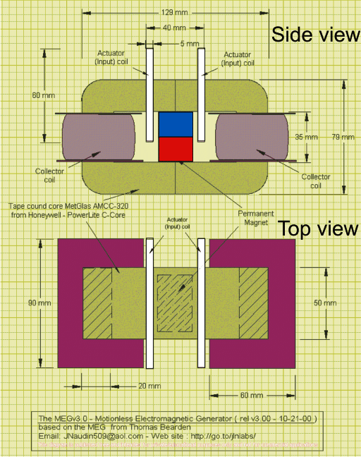
The figure above shows the basic layout or set up of the coils, magnets and the core. The green colored section indicates the ferromagnetic core, which are in the form of 2 C-cores joined edge to edge, like this [ ].
The violet colored items are the collector coils wound over plastic bobbins, these coils react with accumulated, concentrated pulsating magnetic fields and convert them into COP3 electrical energy or COP 3 overunity output.
The white sections indicate the smaller trigger coils which accept the pulsating DC input from an external power supply source.
The central red, blue blocks refer to the magnets which should be preferably neodymium types.
In the image the upper drawing shows the side view of the device while the lower diagram presents the top view of the ME Generator.
The coils indicated in white are required to be pulsated alternately at some specified frequency which could be according to the core specification.
For laminated iron C-cores, the frequency could be anywhere between 50 and 200Hz, this might need some experimentation for figuring out the optimal or the most beneficial outcome, in terms of the COP value.
The following circuit diagram can be effectively used for powering the primary coils, as stated in the above paragraph.
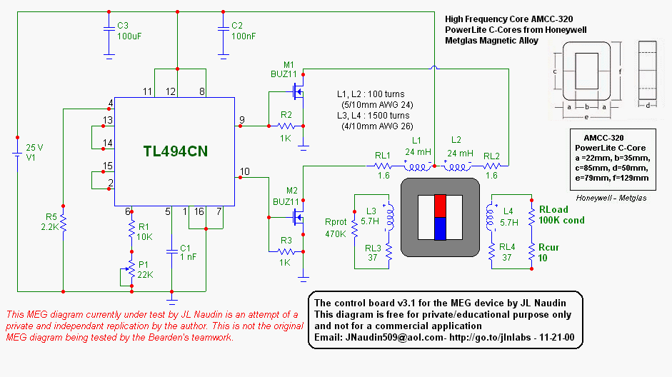
Core Specifications:
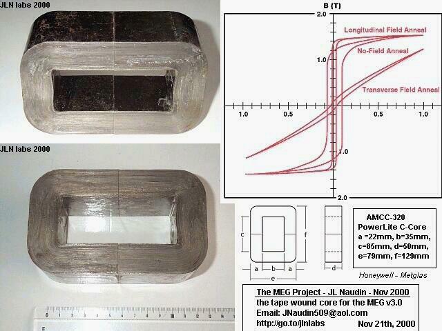
The core used for the MEG can be crucial, the details are furnished in the following image:
Inventors: Patrick Stephen L; Bearden Thomas E.; Hayes James C.; Moore Kenneth D.; Kenny James L.
Appl. No.:656313 Filed:September 6, 2000
by increasing the size of iron core and adding more magnets can it produce 2kw of electrical energy???
please reply..
I am not so sure about it. It will need to be experimented.
First, we have to check whether the above basic design works correctly or not, if it works then we can slowly upgrade it according our needs.
what’s the maximum rating of the Meg ????
can it produces 2kw energy from single Meg???
The maximum power could be around 60 watts, 2kW may not be feasible.
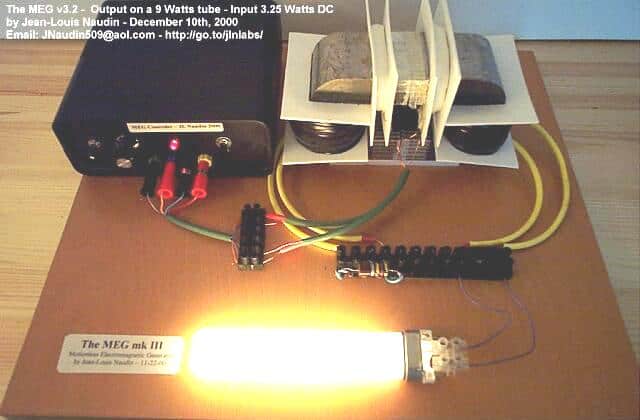
Hi, I built this MEG device, I believe I got it to work as intended. The key is to use a non linear load. Any tests with a linear load such as a resistor will not show over unity.
Next is to find a way to use that output for something useful like powering the MEG device. To date, I do not know if anyone was able to do so.
Hi, thanks so much for updating the results! This sounds fantastic. Please let us know if there are any further developments.
Motionless Electromagnetic Generator
https://patents.google.com/patent/US6362718B1/en
The Motionless Electromagnetic Generator operates in accordance with an extension of Faraday’s Law, indicating that an electrical current is induced within a conductor within a changing magnetic field, even if the source of the magnetic field is stationary.
How does the MEG work?
Consider the physical layout of the MEG. You have a stack of neodymium magnets in the center of a rectangular toroidal core. The magnets touch each side of the core on the inside. There are no coils on the core yet.
What does the magnet flux do?
The flux from the magnets will divide equally between each leg of the core. So you have half the flux flowing on the right and half on the left.
You now place coils on this core. You use two control coils on the top on each side of the magnet stack. And you wind two output coils on each vertical leg on opposite sides.
OK, it is set up. Now you want to switch all the magnet flux to one side by opposing the magnet flux with the opposite control coil. How much flux will the coil need to generate to do this? Well, the answer of course is half the magnet flux since that is what is flowing in that leg. The other control coil is in the off condition, and open circuited, so no current can be induced in it and hence no back-flux generated. The core must not be allowed to reach magnetic saturation or more energy will be required to force the flux to the other side.
Then you turn off the control coil and what happens?
Remember both control coils are now off. The magnet flux will return to its original starting condition of half the flux flowing on each side. Does the magnet need any help to do this? No, of course not. When you did this you also removed half the magnet flux from the other leg when the control coil was on. The first half cycle you only see half the normal induction level in each output coil because at the start you only switch half the magnet flux into one leg and out of the other. So the total change is Bmag/2.
Now on subsequent cycles you let the magnet flux return to its original steady state and let the magnet do the work. Both control coils are off while this happens. Just when the magnet flux reaches its equilibrium point you turn on the other coil and keep the flux change going the other way. Each coil only needs to always switch half the magnet flux not all of it. After the first half cycle you see a 100% change of the magnet flux in each output coil on each cycle for an input power that is half the output. This assumes that you are activating the control coils for half of each cycle. This means you have a theoretical maximum COP of 2.0. You are using the magnet stack as a flux battery and “letting” it do half the work.
So you can get an OverUnity solid state generator with a theoretical maximum gain of 2.0. Just this alone could allow you to reduce your utility bill by about half if you put these devices between your breaker panel and your appliances.
Built a rotoverter.
Please explain more!
Is there a commercially available version of this device.
Hello Swagatam, Thank you for this. I was wondering if you might put me in touch with anyone who has got this to work. The poster “Cycle” did quite a lot of work back in May-June2020. Do you know if he got this to work or how to get in touch with him? We live in some interesting times, and anything potentially good, I would like to support.
Thank you Steve,
I don’t seem to find anybody you has successfully tested and verified the working of the above concept. I have no further information whether Cycle was able to build and confirm the MEG circuit successfully or not. I think if you search on youtube you could find something related with confirmed test results.
Thank you Swagatam for posting this. If you’re interested in actually replication this device please let me know. Would love to discuss.
Thank you John, it would be indeed great if you replicate this project and update the details here. The other visitors here would surely love to read it.
Dear Swagatan,
I am currently in the process of buying all of the components for this.
What’s the wattage rating for the Resistors and Capacitors?
What does P1 stand for and what is the power rating on it?
Thank you so much!
Hi Ryan,
Glad to know you are about to try this circuit.
All the resistors are 1/4 watt 5% But I am not sure about RL1, RL2, RL3, RL4 you can try 2 watt resistors for them.
P1 is variable resistor, also known as a preset or a trimpot. It can be any standard type.
I did not get a notification, but I had this left open on my computer.
Thank you so much for the reply! I will give it a shot!
Sure, no problem.
Let me know if you receive a notification for this reply.
Hi…I’m just getting into this rabbit hole of free energy devices, and this MEG unit is intriguing. My questions are: What components are needed to keep from shorting out a battery/power supply, to get current to a wire coil over a ring magnet? There is also a Caduceus style winding around the magnet-coil ring. The photo of the unit I saw had a 4AA batt pack (5v.) to kick start the windings, but the circuitry was not explained quite enough for me to get it. It had a regular wall outlet connected to the output side where they were getting a 749v. reading on the meter. If you are interested in discussing this or to see a photo of what I have so far, I’m very interested in learning the electric side of things. I am a machinist by trade and can follow descriptions. I just need some help with this circuitry. Thanks…Your articles on here are really helping me understand more about this.
Hi, thanks you, and glad you liked the articles. I understand that you want to learn more about MEG, however due to work load and time constraints it can be difficult for me to delve into this subject and discuss it in details. Moreover I have never tested a free energy machine such as a MEG practically so my expertise is quite limited in this field of electronics
Thanks for your reply, and I understand, I’ll keep looking for something and if i find something I’ll post it back here.
Thank you, appreciate your response!
Hi Jesse,
I have some technical data from another engineer that had posted and worked on replicating this device. Feel free to reach out to me via email, am happy to collaborate, jwrare@gmail.com
I have a question or concern. Why after over 20 years since this MEG patent, has there been NO working model available? In spite of the “claims” including J.Naudin who offered a COP of 3, I believe, early on. The crew that filed the patent seem to have no working model either. Yes, many have claimed an over-unity, but no one seems to have proof. Nor, has anyone offered a product in over two decades. The theory makes sense, yet here we are, with NO evidence that it works. I ran through and reviewed as many video experiments that I could find. In the end, they all just “faded” away, with no conclusions, lol. Any one here have more insight?
I have not yet tested this circuit practically, so it will be difficult for me to suggest anything useful.
In their groundbreaking Motionless Electromagnetic Generator (MEG), they make use of something called the Aharonov-Bohm effect. It’s like a special trick they’ve patented. First, they use this effect to get the area around the transformer all charged up with what they call a curl-free A-potential. Then, they do some normal tweaking to the core, making it send out these A-field perturbations into that charged-up space outside (you know, into its A-potential). The MEG, in return, gets back extra energy in the form of pulses from the E-field, following a simple equation: dA/dt = – E. So, this altered space around the generator, when it gets tweaked again, gives back free E-field energy to the unit. It’s like a two-way exchange, with the local environment chipping in extra energy for free.
Now, when it comes to force fields, those are usually tied to matter because, well, mass plays a big role in it. But, when you’re in space without any mass, there’s no force, according to some smart folks like Richard Feynman. Instead, there’s this thing called “conditions of spacetime” going on, and what we casually call “EM force” is basically just how this spacetime thing interacts with charged stuff.
This dude John Wheeler, he had this cool saying about space and matter. He said, “Space tells matter how to move, and matter tells space how to curve.” Basically, they’re in this back-and-forth dance. Wheeler also threw some shade on elementary particles, saying they’re like a tiny blip in the big picture of vacuum physics.
The Aharonov-Bohm effect, along with some other cool tricks, shows that you can mess with the local spacetime directly. It’s like tweaking the very fabric of where things exist and then using it to influence what’s in that tweaked space.
So, when we say “force,” it’s not some magical thing. It’s just how spacetime conditions chat it up with charged matter. The big takeaway here is that they’ve figured out a way to prep the space around their generator without doing any heavy lifting or using force. Then, they give this energized space a little nudge, and it happily gives back extra energy to power things up. It’s like having two sources of energy: one you put in to create the system and another the space around it chips in for free.
Now, these cool systems that go beyond the usual electrical engineering stuff were purposely left out of the game back in 1892. There was this whole thing about making things symmetrical, thanks to J. P. Morgan. They didn’t want asymmetrical “energy from the active vacuum” systems that Tesla had discovered to mess up their plans. Tesla, he had this dream of getting power from anywhere in the universe, but Morgan shut that down real quick. Instead, we got stuck with more regular power systems like AC.
Tesla was onto something big when he talked about machinery running on energy from everywhere. He wanted methods that didn’t waste any materials and could tap into never-ending stores of energy. Even back in the late 1800s, he believed we were close to making it happen. He envisioned engines running anywhere on Earth, fueled by the energy of the surroundings. Too bad his ideas got sidelined in favor of more traditional power systems.
Hey Barry, good question. I became aware of this type of work via Dr. Steven Greer. He answers your question and has been involved with new energy tech since the early 90s.
They only have a successful prototype. First the transfer functions of the device need to be calculated, then they can make a preproduction model and then they can start massproduction. To calculate the transfer functions is very difficult because you are trying to measure 1 signal in a VERY dens signal environment, you need special equipment and scientists to do this because your average electric engineering PhD is not able to do this. You can find the necessary people and equipment but this is very expensive. Now the meg team is trying to find some risk venture capitalist who will fund the project.
Dear Swagatan,
I am an italian guy with passion for energy…
I would like to solve the problem of energy onboard of my saling boat, as I will live onboard next year…
I saw your meg, is it possible to realize a meg or similar generator of 500w 12v (maximum, I need less energy…)?
Is it possible to find it ready?
I am not be able to realize it… i think
Thank you for your answer
ciao
martino
Hi Martino, I appreciate your interest, and understand that you want to solve your onboard energy problem. However, I have not yet verified the above concept practically, so I can’t actually confirm whether the above circuit really works or not. Therefore it is presently difficult for me to solve your query, I hope somebody else might know more about this concept and help you out with your requirement.
The Motionless Electromagnetic Generator: How It Works.
http://www.rexresearch.com/bearden/BeardenMEGHowworks.doc
EXPLANATION OF THE MOTIONLESS ELECTROMAGNETIC GENERATOR WITH 0(3)
ELECTRODYNAMICS.
http://www.rexresearch.com/bearden/BeardenEXPLANATIONMEG.pdf
Hi Swagatam
My name is Tom Kenefick.
I live in Missouri USA
I saw your circuit that generates motionless high power 110/220 volts AC.
I tried to save it but that did not work.
I would like to power my house to get off the grid.
What is the name or number of your high power generator?
I have seen a lot of generators on the internet but they don’t have the how to details.
Hi Tom,
sorry, can’t remember which circuit you are referring to? There are more than 1300 posts in this blog, so I may have completely forgotten about the one you are looking for….could you provide more specifications of the generator so that I can remember its location?
Hi Swagatam,
As I recall it had a bank of about a dozen light bulbs in the back.
In front there were 3 coils with one slid inside the large one.
It made high power 110 and 220 volts that I want to use to power my house to cut my electric bill or get off the grid.
It is all solid state/motionless.
I don’t think it used a transformer.
Thank You
Tom Kenefck
gtomkx@gmail .com
Hi Tom,
Are you referring to the following article?
https://www.homemade-circuits.com/5kva-ferrite-core-inverter-circuit/
Do you know of anyone anywhere who can make an MEG with a COP of 3?
Sorry, I do not have anybody who would do this practically….
What are the Voltage, current and power ratings for the MEG as built? Can the MEG be upsized for typical household volatge and current? How is this done?
It will depend on the coil wire dimension. I am not sure how it can be upgraded, so can’t confirm it.
It there someplace I can go to get more details? Have you built and tested a MEG? Do you know the Input and Output power limits? What application have you used a NEG for? Does anyone know more about this?
I have not tested this design. For more info you can check out the following link
http://citeseerx.ist.psu.edu/viewdoc/download?doi=10.1.1.129.6448&rep=rep1&type=pdf
You can tweak it so as to produce so much power that you can burn the insulation of the wires
Here’s a simplified circuit to prevent H-bridge shoot-through… the transistor goes foward-active when there is voltage on the H-bridge. Normally, this would be when the pulse voltage to drive the MOSFET gates is off… except during shoot-through. In that situation, the bottom MOSFET dumps voltage off the gates of the two transistors feeding voltage to the H-bridge lower MOSFET gate, preventing shoot-through.
Open both switches to simulate shoot-through without shoot-through protection. Close the bottom switch to activate shoot-through protection.
The 25 kOhm potentiometer is adjusted to give a gate voltage just below the MOSFET’s threshold, so when shoot-through protection is activated, the lower H-bridge MOSFET will not close.
http://tinyurl.com/y94vlsr8
As regards H-bridge shoot-through, I think I’ve found a solution…
http://tinyurl.com/ydyk8urt
In the circuit simulator, hit the “Run / Stop” button (if it doesn’t start running automatically upon page-load).
The top switch is open, simulating the upper MOSFET being closed even when the lower MOSFET is closed… ie: we’re force-simulating shoot-through.
Note the peak amperage on the graph to the right… 861.796 mA when the lower right-hand MOSFET closes. The lower right-hand MOSFET (which would be a part of the H-bridge) is dumping 861.769 mA during this shoot-through event.
Now close the bottom switch. Note that the left-hand MOSFET (the probe-MOSFET, a part of the protective circuitry) is now dumping ~722 nA (average) to ground… that’s the amount of current we have to ‘throw away’ to get the protective circuitry to work properly.
Note that the right-hand MOSFET is now dumping ~2.9 mA (average) to ground… this represents the amount of shoot-through with the protective circuitry in operation. So we’ve lowered the shoot-through by ~858 mA.
Now close the top switch (simulating normal operation)… note that the Vgs (Voltage: Gate To Source) of the lower MOSFETs is 11.936 V (for the protection MOSFET) and 11.988 V (for the lower right-hand MOSFET)… so the protection circuitry only scrubs off 0.064 V and 0.012 V from the gate voltages as compare to if the MOSFETs were driven directly.
Note also that during normal operation, the protective circuitry dumps ~201 nA to ground… that is the ‘cost’ we pay to protect from shoot-through.
I’m sure the circuit can be further improved to lower that ‘cost’. I’ll keep working on it.
Ok, this is the penultimate circuit. I can’t really think of any other enhancements, so this is going to be the one I build.
The changes in this iteration (this is in addition to the changes I’d made from the last iteration):
1) Vgs Protection: I’ve added zener diodes back-to-back on the MOSFET gate and source to protect against excessive Vgs (Voltage: Gate to Source). The zeners start to backbleed at 19 volts. Since MOSFET maximum Vgs is +-20 volts, this will prevent burning out the MOSFETs due to excessive Vgs.
2) Variable Dickson Charge Pumps: The Dickson charge pumps are now variable voltage, using a simple potentiometer voltage divider setup that ranges between (for the positive-voltage Dickson charge pump) battery voltage and the voltage pulses from the 555 timer output; and (for the negative-voltage Dickson charge pump) between ground and the voltage pulses from the 555 timer output. This changes the amount of current each 555 timer output pulse pushes into the storage caps, which changes the resultant voltage applied to the gates of the MOSFETs. It ranges from a few mV up to +-~11.8 V.
3) I got rid of the inductors on the Vin of the 555 timer, and substituted a capacitor array instead. Each cap is a different capacitance, so each absorbs different frequency oscillations, so the voltage at the 555 Vin pin is more stable.
For some reason, inductors really slow down the circuit simulator, so I’ve disconnected them from the circuit and set them aside, replacing them with wires so the circuit could be tested. The wires to the left of the inductors should be removed, and the inductors put in their place if you’re going to build this circuit.
The circuit is now too complicated to get the link shortener to work, so posting a shortened URL is out of the question… most URL shorteners remove some of the components of the circuit, others simply refuse to shorten the URL.
So, I’ll post the component list. You can load the Falstad circuit simulator, click ‘File’ -> ‘Import from text’, and paste this list:
$ 3 0.0000049999999999999996 2.5790339917193066 50 6 50
165 -360 -8 -280 -8 6 0.000023200031681450925
v -440 -72 -440 -128 0 0 40 12 0 0 0.5
c -264 168 -296 168 0 1e-10 -8
s -440 -128 -440 -184 0 0 false
w -192 296 -264 296 0
g -264 168 -248 168 0
c -408 216 -408 248 0 2.2000000000000002e-8 6.327156612922648
w -360 120 -360 88 0
w -264 296 -264 168 0
w -296 152 -296 168 0
w -264 168 -264 152 0
r -232 216 -312 216 0 250000
174 -408 168 -312 136 1 50000 0.5 Frequency Rough Tune
w -408 168 -408 184 0
w -408 184 -360 184 0
w -408 184 -408 216 0
174 -408 216 -312 184 1 500000 0.5 Frequency Fine Tune
w -312 168 -312 216 0
O -232 56 -232 40 0
g -360 24 -360 40 0
w -232 -40 -296 -40 0
c -408 -136 -408 -104 0 2.2000000000000002e-8 5.672843387077353
w -360 136 -360 120 0
w -408 296 -264 296 0
w -360 120 -408 120 0
w -408 120 -408 -104 0
r -408 -184 -408 -136 0 10
w -408 168 -408 120 0
r -408 296 -408 248 0 10
w -408 296 -440 296 0
w -232 -184 -408 -184 0
w -408 -184 -440 -184 0
w -440 -72 -440 296 0
w -232 56 -232 216 0
r -160 56 -232 56 0 20
w -232 -184 -192 -184 0
w -56 -64 0 -64 0
w 0 -64 0 -176 0
w 0 40 0 168 0
34 BAS45A 0 1e-9 10 1 125
d 208 -176 208 -144 2 BAS45A
d 208 -48 208 -80 2 BAS45A
d 208 136 208 168 2 BAS45A
d 208 72 208 40 2 BAS45A
34 VSB2045Y-M3 0 0.000009999999999999999 0.021 2 45
d 208 -176 240 -176 2 VSB2045Y-M3
d 240 -176 272 -176 2 VSB2045Y-M3
d 208 -48 240 -48 2 VSB2045Y-M3
d 240 -48 272 -48 2 VSB2045Y-M3
c 272 -176 272 -48 0 0.000001 -11.569716864279183
r 272 -176 344 -176 0 2
l 392 -176 392 40 0 0.042 0
r 272 -48 336 -48 0 2
d 240 40 208 40 2 VSB2045Y-M3
d 272 40 240 40 2 VSB2045Y-M3
d 240 168 208 168 2 VSB2045Y-M3
d 272 168 240 168 2 VSB2045Y-M3
r 272 168 336 168 0 2
l 376 168 376 -48 0 0.042 0
r 272 40 344 40 0 2
w 64 72 64 168 0
w 64 -144 64 -48 0
w -160 56 64 56 0
w 208 -112 88 -112 0
w 88 -112 88 -184 0
w 88 104 88 296 0
w -192 296 88 296 0
w 64 56 64 -48 0
w 32 -176 0 -176 0
w 32 -80 16 -80 0
w 32 168 0 168 0
w 32 72 32 136 0
w 208 104 88 104 0
w 32 72 16 72 0
w 16 72 16 -80 0
w -24 -184 88 -184 0
w -56 -64 -56 -120 0
w -72 -184 -192 -184 0
d -40 -184 -72 -184 2 BAS45A
r 144 -128 96 -128 0 10
r 144 -96 96 -96 0 10
r 144 88 96 88 0 10
r 144 120 96 120 0 10
w 144 -128 144 -160 0
w 144 -64 144 -96 0
w 144 88 144 56 0
w 144 152 144 120 0
w 96 -128 96 -160 0
w 96 -64 96 -96 0
w 96 88 96 56 0
w 96 152 96 120 0
d 144 152 96 152 2 VSB2045Y-M3
d 144 56 96 56 2 VSB2045Y-M3
d 96 -64 144 -64 2 VSB2045Y-M3
d 96 -160 144 -160 2 VSB2045Y-M3
w 192 -176 208 -176 0
w 192 -144 208 -144 0
w 192 -80 208 -80 0
w 192 -48 208 -48 0
w 192 40 208 40 0
w 192 72 208 72 0
w 192 136 208 136 0
w 192 168 208 168 0
f 144 -160 192 -160 41 2.5 2.9629629629629632
f 144 152 192 152 40 3 6.609385327164574
x 185 228 277 231 4 8 p-MOSFET:\sSUP70101EL
f 144 -64 192 -64 33 2.5 2.962962963
x 185 202 273 205 4 8 n-MOSFET:\sSUP70090E
f 144 56 192 56 32 3 6.6093853272
f -56 -120 -56 -168 40 3 6.6093853272
w -40 -168 -40 -184 0
w -72 -168 -72 -184 0
c 240 -24 240 16 0 0.000002 11.999993868535267
w 240 104 208 104 0
w 240 -24 240 -112 0
w 240 -112 208 -112 0
w 240 104 240 16 0
w 0 40 32 40 0
w 336 -48 336 168 0
w 344 -176 344 40 0
c -272 -56 -232 -56 0 1e-10 -12
c -272 -88 -232 -88 0 1e-9 -12
c -272 -120 -232 -120 0 1e-8 -12
c -272 -152 -232 -152 0 1.0000000000000001e-7 -12
w -232 -184 -232 -152 0
w -232 -152 -232 -120 0
w -232 -120 -232 -88 0
w -232 -88 -232 -56 0
w -232 -56 -232 -40 0
g -320 -56 -328 -56 0
g -320 -88 -328 -88 0
g -320 -120 -328 -120 0
g -320 -152 -328 -152 0
r -272 -152 -320 -152 0 10
r -272 -120 -320 -120 0 10
r -272 -88 -320 -88 0 10
r -272 -56 -320 -56 0 10
w 64 72 64 56 0
160 96 56 32 56 0 5 10000000000
160 96 152 32 152 0 5 10000000000
160 96 -64 32 -64 0 5 10000000000
160 96 -160 32 -160 0 5 10000000000
w 208 120 208 104 0
w 208 88 208 104 0
34 Gate\sProtection\sZener 0 5.0000000000000004e-8 0 2 20
z 208 120 176 120 2 Gate\sProtection\sZener
z 144 120 176 120 2 Gate\sProtection\sZener
w 208 120 208 136 0
z 208 88 176 88 2 Gate\sProtection\sZener
z 144 88 176 88 2 Gate\sProtection\sZener
w 208 88 208 72 0
w 208 -128 208 -144 0
w 208 -80 208 -96 0
z 208 -96 176 -96 2 Gate\sProtection\sZener
z 144 -96 176 -96 2 Gate\sProtection\sZener
z 208 -128 176 -128 2 Gate\sProtection\sZener
z 144 -128 176 -128 2 Gate\sProtection\sZener
w 0 -48 32 -48 0
w 32 -80 32 -144 0
w 0 40 0 -48 0
w 0 -48 0 -64 0
w 208 -112 208 -128 0
w 208 -96 208 -112 0
w 32 232 32 136 0
w -192 264 -144 264 0
r -192 200 -144 200 0 5000
d -192 200 -192 264 2 BAS45A
c -192 144 -192 200 0 4e-10 0.008771991028985661
w -56 232 32 232 0
w -144 -152 -192 -152 0
r -192 -88 -144 -88 0 5000
d -104 -120 -56 -120 2 BAS45A
g -56 -32 -56 -24 0
174 -144 -88 -104 -144 1 1000000 0.1733 Positive Gate Bias
d -192 -152 -192 -88 2 BAS45A
c -56 -64 -56 -32 0 1.0000000000000001e-7 16.73060674960013
c -192 -24 -192 -88 0 4e-10 -12.007789212327163
w -192 -184 -192 -152 0
w -192 32 -160 32 0
w -160 32 -160 56 0
174 -144 264 -104 208 1 1000000 0.8168000000000001 Negative Gate Bias
w -160 56 -160 80 0
w -192 80 -160 80 0
d -56 232 -104 232 2 BAS45A
g -56 200 -56 192 0
c -56 232 -56 200 0 1.0000000000000001e-7 -5.474694732412012
r -232 24 -232 -40 0 100000
z -24 -184 -24 -152 2 Gate\sProtection\sZener
z -24 -120 -24 -152 2 Gate\sProtection\sZener
w -24 -184 -40 -184 0
w -24 -120 -56 -120 0
w -192 264 -192 296 0
w -192 32 -192 -24 0
w -192 144 -192 80 0
o 18 32 0 45322 11.999985336343562 0.0001 0 1
o 47 32 0 12546 11.769100951821793 0.0001 1 2 47 3
o 172 32 0 12546 16.735206319146293 0.0001 2 2 182 0
That looks awesome, thank you very much!
I’m having trouble finding an analog switch which will fill the bill… of the analog switches I’ve researched, either they can’t switch negative voltages, require a dual (positive and negative) power supply, don’t have the voltage range needed (they can only handle logic-level input), they’re make-before-break, etc.
The Vishay DG449 looks pretty good, though… it’s SPDT, it can handle switching +-15 volt analog signals, can handle a continuous 30 mA (which should be plenty for switching 4 MOSFETs), has a faster turn-off time (58 nS) than turn-on time (133 nS) (so it’s break-before-make), and does all that with a typical current consumption of ~7uA.
https://www.digchip.com/datasheets/parts/datasheet/513/DG449-pdf.php
I’m considering connecting the V+ and NC pins, and the V- and NO pins, so the charge pump positive and negative voltages provide the voltage to run the analog switch. This way, as the charge pump voltage increases, the analog switch has sufficient voltage to switch the voltage at the NC and NO pins.
What do you think, Swagatam? Would that work?
Barring that, Pickering has some break-before-make SPDT mercury-wetted reed relays that operate on 12 V at ~6 mA (it would be triggered from the 555 timer output), and since the contacts are mercury-wetted, it should have an operational life in the billions of cycles. It’d be old-school, but it’d do away with the problems of switching negative voltages with FETs.
I tried making my own analog switch… it worked, after a fashion… I got the necessary output voltages to drive two of the MOSFETs, and the inverted voltage to drive the other two MOSFETs when using a regulated supply for positive and negative voltages, but the drain was too high when connecting it to the Dickson charge pumps, and they couldn’t maintain sufficient voltage. And I got a nasty flow-through from positive-to-negative just as the circuit was starting up. Discrete components designed for switching higher amperage have too much leakage to work as an analog switch, I think.
Well, I worked on my analog switch a bit more… I got shoot-through down into the low uA range, and the charge pumps can now build voltage.
The Homebrew Analog Switch has regular and inverted outputs, to drive 4 MOSFETs in an H-bridge.
So the outputs would be like this:
Output 1: + – + – + -, etc., etc. (drives one pMOSFET on high side and one nMOSFET on low side of H-bridge)
Output 2: – + – + – +, etc., etc. (drives the other pMOSFET on high side and nMOSFET on low side of H-bridge)
And it works with positive and negative voltages, so the MOSFET gates are driven harder, to slam the MOSFETs open and closed in a shorter amount of time, to lessen heating.
If you slow the circuit simulator way down to 1 pS per interval, you’ll see there’s still shoot-through on the MOSFETs as the circuit starts up, but it goes into the negative-voltage Dickson charge pump storage capacitor… so at least it’s not a dead short to ground. After the 555 timer cycles a couple times, sufficient voltage is built up in the Dickson charge pump storage capacitors that the analog switch MOSFETs settle down and start operating correctly.
Since the Dickson charge pumps are now operating 8 MOSFETs, rather than the previous 4, I’ve got to run it a bit harder than before. I’ve increased the pump capacitor size to 20 nF, and the storage capacitor size to 500 nF to compensate.
You’ll note there are two switches in the circuit now… those are pushbutton switches to bypass the Dickson charge pump voltage divider variable resistor (used to vary the charge pump output voltage), which increases charge pump voltage much faster. Push it for about half a second of circuit simulator run-time, and you’re up to operating voltage. If you push one button, the other depresses, as well, and vice versa. On the PCB I’m laying out, I’ve put two screw-terminals for the wires to these switches (actually, a single DPST momentary-contact pushbutton switch), which will be mounted on the front face of the case.
Here’s the section of the MEG driver circuit with the Dickson charge pumps and the homebrew analog switches:
http://tinyurl.com/yaljcoll
And here’s an image of the new homebrew analog switch working in the MEG driver circuitry:
" rel="nofollow ugc">
I’ve updated the models for the MOSFETs to more accurately reflect actual MOSFETs. I modeled after a SUP70101EL p-MOSFET and a SUP70090E n-MOSFET. I slowed the time step of the circuit simulator down to 1 ps, and watched the circuit, which uncovered some issues. The fixes below address those issues.
Ok, a guided tour of the much-improved circuit:
http://tinyurl.com/yadlfsds
1) The 22 nF capacitors and 10 Ohm resistors to the left of the circuit:
This is to set the 555 timer threshold / trigger voltage to 6 volts when the circuit is first fired up. It reaches 6 volts nearly instantaneously (within 1 ps) since it’s across the battery, but it takes awhile (~2.4 us) for the 22 nF caps to fill. Threshold / trigger voltage doesn’t waver from 6 volts the whole time the 22 nF caps are charging up, except for the amount drained off to trigger the 555 timer. Since the 555 timer threshold / trigger voltage starts at 6 volts, it doesn’t take long for it to drain down to 4 volts to get that first trigger of the 555 timer, and thus to get the circuit running. The 10 Ohm resistors are to damp the oscillations as the 22 nF capacitors charge up.
2) The 15 nH inductor and 30 nH inductor (and resistors to simulate inductor resistance) and the 75 nF capacitor at the 555 timer Vin:
This absorbs supply voltage fluctuations caused by MOSFET switching, so the 555 timer has a more stable supply voltage.
3) The 250 pF capacitor, 50 nF capacitor and zener diode in the upper-center part of the circuit:
This is the positive-voltage single-stage Dickson charge pump. It takes 12 volts from the battery, combines it with the 12 volt fluctuations from the 555 timer output (through the 250 pF capacitor), and produces ~17.85 volts to drive the MOSFET gates.
The zener diode limits maximum positive voltage to ~17.85 volts. This is nearly ideal, since the MOSFETs have a maximum Vgs (Voltage: Gate to Source) voltage of +-20 V.
4) The 250 pF capacitor, 50 nF capacitor and zener diode in the lower-center part of the circuit:
This is the negative-voltage single-stage Dickson charge pump. It generates ~-6.2 volts, which reduces MOSFET switching time and thus reduces MOSFET heating.
The zener diode limits minimum negative voltage to ~-6.2 volts. This is nearly ideal, since the MOSFETs have a maximum Vgs (Voltage: Gate to Source) voltage of +-20 V, and this gives a Vgs of ~-18.2 volts on the p-MOSFETs to turn them on, and ~-6.2 volts on the n-MOSFETs to turn them off.
5) The n-MOSFET at the top-center of the circuit:
This MOSFET’s gate is driven from the positive-voltage Dickson charge pump. It acts as a timer that only turns on when the positive-voltage Dickson charge pump has developed sufficient voltage to drive the MOSFETs in the capacitor / inductor section. This minimizes the likelihood of burning out the MOSFETs in the capacitor / inductor section as the circuit first starts up. It’ll cycle on and off in saturation mode until the positive-voltage Dickson charge pump voltage reaches Vbat + Vt = 15 volts, then this MOSFET will be always-on in linear mode. So this MOSFET is going to need a good heatsink, as it’ll likely heat up as the circuit starts up.
6) The capacitor / inductor section at the top-right of the circuit:
This is an H-bridge which shunts battery voltage back and forth across the 1 uF capacitor, through the 42 mH inductors (which are analogous to the MEG drive coils).
The positive voltage from the positive-voltage Dickson charge pump and negative voltage from the negative-voltage Dickson charge pump are applied to the MOSFET gates via SPDT analog switches which are triggered from the 555 timer output. This isolates the 555 timer from the MOSFETs (and thus from the high voltage developed in the capacitor / inductor section should a MOSFET short out), and reduces switching time of the MOSFETs.
The p-MOSFETs are modeled after the SUP70101EL and the n-MOSFETs are modeled after the SUP70090E.
The flyback diodes across the MOSFETs are modeled after the BAS45A, an extremely low back-leakage diode. MOSFETs usually already have an internal flyback diode, so the external diode is backup to the internal diode.
The diodes protecting the MOSFETs from high voltage spikes are modeled after the VSB2045Y-M3, which has extremely low serial resistance. Voltage swings in the capacitor / inductor section are high enough that two of these diodes in series are required at the entrance and exit of the capacitor / inductor section.
The diode / resistor on the gate of each MOSFET is to prevent the MOSFETs on one side of the H-bridge from both being on at the same time, which represents a short circuit. It does this by charging the p-MOSFET gates faster than it discharges them, and by discharging the n-MOSFET gates faster than it charges them.
It is important to keep the components feeding the MOSFET gates as near together and as close to the MOSFET gates as possible. This reduces capacitance in that part of the circuit, which decreases MOSFET switching time and thus MOSFET heating. It also reduces ringing when the MOSFETs open and close, which can cause false triggers of the MOSFETs.
7) The 2 uF capacitor in the capacitor / inductor section is a ‘surge tank’… it just ensures voltage is as near to battery voltage when the MOSFETs open, to get wider voltage swings in the inductors.
Here’s the same circuit as my last one, but optimized a bit more.
http://tinyurl.com/y7fytnab
I edited the diode model for the BAS45A and VSB2045Y-M3 diodes to more accurately reflect their serial resistance, and I used two of the VSB2045Y-M3 diodes in series at the entrance to and exit from the capacitor / inductor section… this is because with the new, more accurate serial resistance model of the VSB2045Y-M3 diodes, the voltage swings in the capacitor / inductor section were too high for a single diode to handle. I’d overestimated the VSB2045Y-M3’s serial resistance… it’s a moderate voltage (45 V) and moderate amperage (20 A) diode, but with extremely low serial resistance.
The BAS45A is a high voltage (125 V), low-amperage (624 mA) diode, but with ultra-low bleedback (1 nA), which is why I used it in the negative voltage section (the section which drives the MOSFET gates for half of each cycle). I’d underestimated its serial resistance… it’s very low bleedback, but very high resistance.
I also discovered that this circuit has a maximum capacitance that you can use… with the 42 mH coils and at 60 Hz, it’s 84 uF. That’s at exact resonance at 60 Hz. Above that capacitance, it takes longer for the cap to drain and fill than the cycle time of the 555 timer, and the circuit ends up fighting itself.
At the maximum capacitance, you’ll get ~+-61.5 V swings in the 84 uF cap (123 V peak-to-peak), and you’ll be pushing ~2.74 A through the coils on each pulse, with the circuit drawing an average of ~15 watts. That’s far more than enough to do what we want to do.
Again, this circuit is not a resonant circuit… if you want less current through your coils, reduce the size of the center capacitor; if you want more current through your coils, increase the size of the center capacitor (not to exceed 84 uF for 42 mH coils at 60 Hz… you’ll have to calculate the maximum size of the cap for the inductance of your coils at the frequency you’re running).
I also altered the center section (the zener diodes) a bit to reduce the negative voltage… it had been drawing voltage down too far, exceeding the 20 volt Vgs (voltage:gate to source) limitation on the MOSFETs.
As regards the charge pump capacitors: the performance of the circuit is highly correlated to the size of the charge pump capacitors.
In the negative-voltage section of the circuit, you have a charge pump cap and a storage cap.
The larger the storage cap, the narrower the voltage swings and the longer it takes to reach the final negative voltage the circuit will run at. You want some voltage swing on that storage cap, the MOSFETs need it to be protected from excessive Vgs (voltage:gate to source). Ideally, you’d size the storage cap so you had zero volts or a very small negative voltage just as the MOSFET closed, then the charge pump capacitor would pull the storage cap low.
The charge pump caps are what affects circuit performance. The larger the charge pump caps, the faster the negative voltage will reach its final working voltage, but that affects the magnitude of the voltage swings in the central capacitor which drives the inductors.
The difference in capacitance between the charge pump cap and the storage cap determines how low the negative voltage will be pulled. You can size the charge pump cap too small, to the point that it doesn’t pull voltage down fast enough to offset the leakage current through the analog switches, and thus negative voltage doesn’t build up. You can size it too large, and the negative voltage builds up to the point that you damage the MOSFETs via excessive Vgs (voltage:gate to source).
So you want to size both the storage cap and the charge pump cap as small as possible (but still large enough to pull a tiny bit more than the analog switch leakage current), with the ratio between their sizes just enough to get voltage down to around -6 volts.
That’ll give you ~-18 volts Vgs on the p-MOSFET gates (the p-MOSFETs are at the entrance to the capacitor/inductor section), and ~-6 volts on the n-MOSFET gates (the n-MOSFETS are at the exit to the capacitor/inductor section). This allows the MOSFETS to slam fully open and shut, increasing current through the inductors without any false triggers (ie: a MOSFET opening or closing spuriously due to insufficient Vgs voltage differential.
Getting it perfect is an exercise in fine tuning.
In the latest iteration of the circuit, I swapped the wires on the charge pump section so the side with the MOSFETs operating on negative voltage corresponded to the side being pulled low. This allowed me to reduce the size of the charge pump and storage caps, which increased the performance of the circuit.
Rather than ~61.5 volt swings on the maximum 84 uF center cap size, it now goes to 66.176 V; rather than 2.74 A through the inductors, it now pushes 2.949 A through, with the circuit using an average of 15.983 watts.
http://tinyurl.com/y9t7n8g4
If you size the center cap at 500 nF, you’ll get ~322 mA through the inductors, a voltage swing of ~102.35 V on the center cap (~204.7 V peak-to-peak), and the circuit draws an average of ~165 mW.
http://tinyurl.com/y96bnp9d
Well, I didn’t think I’d be able to optimize the circuit more than I’d already done, but I managed to clean it up and fix a few more issues.
This iteration uses two single-stage Dickson charge pumps to produce the + and – voltage for the MOSFET gates, and those charge pumps are driven from the output of the 555 timer rather than from the voltage swings in the capacitor/inductor section as in the last iteration of the circuit. This allows a much finer control over the final voltage that the MOSFET gates see, ensures MOSFET gate voltage is such that the MOSFETs slam fully open and closed without misfiring, and since we’re not draining voltage off the capacitor/inductor section to run the charge pump, the voltage swings are higher. The two zener diodes in the charge pumps set the maximum voltage at the MOSFET gates such that Vgs (voltage: gate to source) doesn’t exceed 20 V.
The positive-voltage charge pump puts out ~17.85 V, and the negative-voltage charge pump puts out ~-6.2 V. That’s just about perfect to run the MOSFET gates.
I also cleaned up the circuit layout a bit.
" rel="nofollow ugc">
Here’s the shortened URL to the circuit simulator with this circuit loaded:
http://tinyurl.com/yajp44p9
It’s a complex circuit for this circuit simulator, so it runs pretty slowly. If a dialog box pops up telling you that the page is unresponsive, wait until it clears automatically. Then the circuit will run.
And the final iteration of the circuit… it’s about as optimized as I can get it.
I changed the 44 nF capacitor used to time the 555 cycles so that it referenced from positive voltage rather than ground. Thus, as soon as the circuit is turned on, the battery voltage rushes into the 44 nF capacitor to build up voltage at the 555 chip’s threshold and trigger pins…. thus the circuit no longer has that long wait right after startup (as voltage builds up in the 44 nF cap to the point that the 555’s threshold and trigger pins have sufficient voltage to operate) before it starts cycling, it starts cycling nearly immediately.
This MEG driver circuit works from 9.6 V to 14.2 V (voltage range of a typical 12 V battery, from dead to fully charged), and from 5 nF to 84 uF for the center capacitor, and protects the MOSFETs from excessive Vgs (voltage: gate to source) throughout that battery voltage range and center capacitor size range.
It is not a resonant circuit unless the center cap is 84 uF (the inductance and frequency determine the maximum center cap size, which is at the point of resonance), it is a brute-force circuit. It automatically goes to 50% duty cycle, and is designed to run at 60 Hz. So for this circuit, running at 60 Hz, with 42 mH inductors (the MEG drive coils), the maximum center cap size is 84 uF. You’ll have to calculate maximum center cap size for your inductance and frequency.
The minimum center cap size is 5 nF because the charge pump section’s storage caps are 5 nF… you can’t go much lower than that for center cap size without the circuit being unable to properly pull negative voltage in the charge pump section, which affects the performance of the MOSFETs.
The size of the center capacitor determines the current that is pushed through the inductors. If you need less, reduce the size of the center capacitor (to a minimum of 5 nF), if you need more, increase the size of the center capacitor (to a maximum of 84 uF for this inductance and frequency).
http://tinyurl.com/ydxs3swo
Ok, here’s another 555 circuit. This one doesn’t rely upon resonance in the capacitor / inductor section… it forces the current through regardless of whether the 555 timer is resonant with the capacitor / inductor section.
This one also doesn’t swing the inductor voltage in both directions, so to get it to work with my setup (a spirally-wound coil in-line with the magnetic flux path), I’d have to set it up so that the energized coil bucked the magnetic flux, then rely upon the in-rush of magnetic flux through the core to unpin and flip the domains in the ferromagnetic material in the opposite coil.
If you find you need more current through the inductors, you can increase the capacitor size. Again, this is not a resonant circuit, it’s a brute-force circuit.
You’ll note the voltage swings in the 5 uF capacitor are more square-wavish than sinusoidal. You’ll also note the circuit is working with 4 Ohms of resistance per coil… that’s much more realistic than my prior attempts.
Here’s a shortcut to the Falstad circuit simulator with this circuit loaded:
http://tinyurl.com/yaol6lex
This circuit also has protective components to prevent the MOSFET Vgs (voltage:gate to source) from exceeding ~20 volts (a common limitation in most MOSFETs)… that’s the mess of diodes / capacitors / zeners in the middle.
The 100 nF and 500 nF capacitors act as a ‘charge pump’… a voltage swing in the 5 uF capacitor will push electrons in the ‘charge pump’ section out through the diode to ground, then when the voltage swings the other way in the 5 uF capacitor, that results in a negative voltage in the 500 nF capacitor.
Those two capacitors also act as a sort of voltage divider… because the one doing the ‘pumping’ (the 100 nF cap) is smaller than the storage cap (the 500 nF cap), the magnitude of the voltage swings on the 5 uF capacitor is divided so the voltage swings in the storage cap (the 500 nF cap) isn’t as wide. The voltage swings in the 500 nF cap are by design… we want voltage to swing like that… that’s what the MOSFETs need.
The zener diodes clamp the negative voltage to a minimum of ~-18 volts, and due to the ‘pumping’ of the 100 nF cap, the voltage waveform is nearly exactly what the MOSFETs need at any given moment (voltage at the MOSFET gates should track with the changes in source voltage, but be x volts lower, but not exceed 20 volts differential between gate and source).
The graphs:
– The left-hand graph is the 555 timer output.
– The second-from-left is the voltage swings in the 5 uF capacitor.
– The second-from-right is the negative voltage used to drive the MOSFET gates. (Positive voltage is taken directly from the battery… the switching between positive and negative is done via analog switches driven by the 555 timer output).
– The right-hand graph is power drain from the battery.
I like this circuit, because it gets up and runs right from the get-go… there’s very little waiting around for voltage swings to build up, as in my prior circuit… within three cycles, it’s at full voltage swing (with the 5 uF capacitor, the voltage swings between +-60.951 V, for a total peak-to-peak voltage of 121.902 V. This gives a short, sharp current pulse on the inductors (equivalent to the MEG drive coils) of 577 mA per pulse). And with all that, the circuit draws less than ~850 mW.
" rel="nofollow ugc">
I’ve been researching how to build a proper MOSFET driver… if I get it working, I’ll post the circuit simulator of it working in the MEG circuit.
As to using a transistor as an ultra-low bleedback diode, here’s the wiring diagram for PNP and NPN type transistors:
" rel="nofollow ugc">
Just learned that in order to do what I’d wanted to do (make the resonant frequency of the inductor / capacitor section trigger the 555 timer, so no matter what the resonant frequency is, the 555 timer would run at that frequency), I need a zero-crossing detector. An XOR gate would seem to fit the bill, but that’s for logic-level (usually 5 volts) signals, not a widely-ranging voltage like in the inductor / capacitor section.
But I put an XOR gate in the circuit to test it… triggered off the 0 crossing of one side of the inductors. It turns on and off at almost exactly the same time at the 555 timer.
This might not be worth it… the problem is getting the inductor / capacitor section oscillating in the first place… when it’s first switched on, there’s no oscillations in the inductor / capacitor section, thus nothing driving the 555 timer, thus nothing driving the oscillations, etc.
Well, I tried to get the 555 timer to trigger from the resonant frequency of the inductor/capacitor section… the trouble is, the waveform on the inductor/capacitor section is only half the wavelength needed to properly trigger the 555 chip. I got it to turn off at exactly the same time as the manual timer does, but it’d always turn on earlier.
I tried a MOSFET inverter (http://falstad.com/circuit/circuitjs.html?cct=$+0+0.000005+10.20027730826997+50+5+50f+208+176+272+176+1+1.5+0.02f+208+272+272+272+0+1.5+0.02w+272+192+272+224+0w+272+224+272+256+0w+208+176+208+224+0w+208+224+208+272+0L+208+224+160+224+0+1+false+5+0M+272+224+336+224+0+2.5R+272+160+272+112+0+0+40+5+0+0+0.5g+272+288+272+320+0) to separate the wide voltage swings of the inductor/capacitor section from the 555 trigger… the inductor/capacitor section drove the MOSFET inverter gates, and battery voltage was used as the 555 trigger. When voltage at the MOSFET gates went too low or too high, six zener diodes in series (three facing one direction, the other three the opposite direction), connected to ground, would damp the voltage swing on the MOSFET gates to +/-17 volts. The MOSFET inverter worked well enough, but it was just the wrong waveform to use.
So, I went back to the drawing board… I realized I didn’t need a duty cycle adjustment, since this is designed for a 50% duty cycle at all times. So now the output of the 555 is the trigger for the 555, and there are two frequency adjustments, one rough and one fine adjustment. This naturally tends toward 50% duty cycle.
I added resistors in between the inductors and the capacitor in the inductor/capacitor section, to make the simulation more realistic… since the spirally-wound coils will be in-line with the magnetic flux, I plan on stacking as many as needed on each side to get efficient flux path switching, and wire the coils on each side in parallel, so the total resistance will be low (plus the wire I’m using is silver-coated, so it’s already pretty low-resistance). I’ve used 2 Ohms in the simulation (1 Ohm resistor on each side of each coil). Without those resistors, the voltage swings on the inductor/capacitor section easily exceeds 200 volts… that’s not realistic.
I used an old trick to replace the diodes which pull a negative voltage (on either side of the inductor / capacitor section)… I replaced the diodes with transistors. This gives ultra-low leakage, allowing the voltage to be drawn down in the caps, which opens the MOSFETs more when the circuit is just getting started, which builds the voltage swings in the inductor / capacitor section more quickly. The transistors switch between cut-off and reverse-active in accord with the voltage across them. You could buy an expensive diode like the BAS454A (1nA reverse leakage at 125V), or you could use a transistor (~0.2 pA reverse leakage @ 16.6 V), which is pretty close to that in performance and is dead cheap. This shouldn’t be used for moving a lot of current, but for this purpose (pulling a couple small capacitors low), it suffices.
" rel="nofollow ugc">
The top-left graph is one of the inductors in the inductor/capacitor section. Due to the more-realistic resistance introduced, this is as high as the inductor voltage will swing. The more inductance your coils have, the more resistance they can have and still perform OK… resistance is the big bugaboo in circuits like this.
The top-middle graph is the negative voltage caps used to help slam the MOSFETs open and shut.
The top-right graph is the power drain from the battery. If inductor voltage went higher than where it topped out, you’d see the downward spikes get narrower and narrower until there is a short, sharp spike downward once per half-cycle, and as inductor voltage swings increase, the power in each of those spikes increases. If we could somehow get around resistance, those coils could easily exceed 200 V swings with just a sharp spike every half-cycle from the battery to drive it.
The bottom graph is the 555 timer output. The graph shows 59.981 Hz, 60.024 Hz and 60.038 Hz when fiddling with the Frequency Fine Tune to try to get exactly 60 Hz. I’ve never seen it settle on exactly 60 Hz, so it may not be able to. You’ll know the 555 timer is near perfect resonance with the inductor / capacitor section when the voltage swings in the inductor/capacitor section exceed the battery voltage.
Thanks for your the efforts and the researches in the field, I appreciate it very much!
Just posting this on the 29 Sept 2021 to see which is the latest post and what direction they are listed in, as none show a date!
The upper comments are the latest ones, the lower ones are the older ones.
I’ve altered my circuitry somewhat… I added a diode and capacitor on each side of the inductor / capacitor part… when it’s in resonance, the low side pulls the capacitor voltage lower and lower.
I also learned that p-MOSFETs are best used on the high side of a load, whereas n-MOSFETs are best used on the low side of a load, so my H-bridge has that now.
I then use that low (negative) voltage stored in the capacitors to slam shut the n-MOSFETs and slam open the p-MOSFETs.
I use analog switches to switch between 12 volts (from the battery) and the negative voltage in the capacitors. The drive circuitry now just drives the analog switches. This gives a nearly perfect square wave output, since there’s no voltage drain on the 555 timer output. This is somewhat akin to a Darlington pair for transistors, with the added advantage that the MOSFETs have positive and negative voltages applied to their gates, so they definitively slam open and shut. I call this setup a MEG Darlington Pair.
With the changes, the circuit drives the inductors (equivalent to the drive coils on the MEG) much harder now, so the voltage swings build up higher and faster, which is my aim… to get the inductor / capacitor part oscillating in resonance such that the voltage swings are as wide as possible, which ultimately lowers the amount of current the drive circuitry has to feed into the inductors to keep them going, and causes more efficient magnetic flux path switching.
The circuit is essentially a parametric oscillator… think of a child on a swing. You push them when they reach the high point (ie: when their velocity reaches zero in either direction), and that keeps the swing going… same thing here. The circuitry switches the MOSFETs when the voltage waveform on the inductors is crossing the zero point.
This is all predicated upon carefully sizing components such as capacitors and inductors such that their resonant frequency is equal to the driving frequency. That’s a bit of a pain to do.
My next goal is to make it a parametric oscillator which uses the resonant frequency of the inductor / capacitor part of the circuit to trigger the driving circuitry… then, no matter what the resonant frequency is, it’ll seek to that frequency and go into parametric oscillator mode. I plan on doing that by referencing the 555 trigger from the voltage swings in the inductor / capacitor part of the circuit. That should greatly simplify the circuit, as well (there will be no frequency adjustment, just a duty cycle adjustment).
Here’s an image of the circuit after it’s run in a circuit simulator for the equivalent of a couple seconds: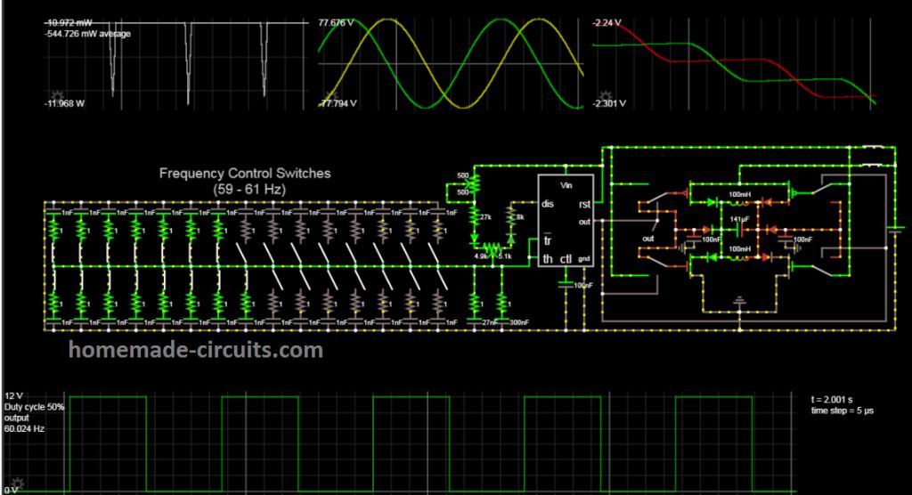
" rel="ugc">
The top-left graph is power drain from the battery. The downward spikes successively narrow as the voltage swings in the inductor / capacitor part of the circuit build up.
The top-middle graph is one of the inductors (equivalent to one of the drive coils in the MEG). The voltage swings successively build up, far above the 12 volts driving the inductor / capacitor section.
The top-right graph is the negative voltage on the capacitors to the left and right of the inductor / capacitor section, used to control the MOSFETs via the analog switches. As voltage swing increases in the inductor / capacitor section, the capacitor voltages go increasingly negative.
The bottom graph is the output of the 555 timer.
Of course, with the inductors actually doing work to switch magnetic flux, the battery drain is going to be higher.
Also, if you place a capacitor across your drive coils, you get a nice sinusoidal wave with the proper lag between voltage and current, which gives a proper sinusoidal output from the output coils. It also “recycles” some of the energy if you size the capacitor to be resonant with the frequency used and the Henries of the driven coils, so the driven coils will actually experience wider voltage swings than provided by the battery due to that resonance. So you’ll see the power drawn from the battery to power the coils goes down as you dial in the frequency so it hits that resonant spot, and that power is just sloshing back and forth from capacitor to driven coils, back to capacitor, back to driven coils, etc.
The way I’m doing it is using the circuitry (similar to above, but using a 555 timer) to drive an H-bridge composed of two n-MOSFETs and two p-MOSFETS. Be sure to place ‘kickback’ diodes across the MOSFETS, and a diode between each MOSFET and the driven coils, to protect the MOSFETs.
Here’s a circuit simulator of my setup (yes, that’s all one long URL, it loads the components into the circuit simulator):
http://falstad.com/circuit/circuitjs.html?cct=$+1+0.000005+1.0751013186076355+35+5+50%0A165+-128+64+-48+64+6+0%0Av+-1008+96+-1008+32+0+0+40+12+0+0+0.5%0Aw+-224+32+-64+32+0%0Ar+-224+32+-224+80+0+6000%0Aw+-224+32+-928+32+0%0Ad+-224+80+-224+128+2+default%0Ad+-160+128+-160+96+2+default%0A174+-224+128+-176+160+1+10000+0.5396000000000001+Duty+Cycle%0Aw+-160+96+-128+96+0%0Aw+-128+160+-176+160+0%0Aw+-176+160+-176+208+0%0Aw+-176+160+-192+160+0%0Aw+0+96+0+32+0%0Aw+0+32+-64+32+0%0AO+0+128+16+176+0%0Ac+-64+224+-64+256+0+1e-7+0.001%0Aw+-32+224+-32+272+0%0Aw+-32+272+-64+272+0%0Aw+-64+272+-64+256+0%0Aw+-1008+96+-1008+320+0%0Aw+-176+320+-64+320+0%0Ac+-176+288+-176+320+0+9.000000000000001e-7+0.001%0Aw+-176+208+-176+256+0%0Aw+-64+272+-64+320+0%0Aw+-128+192+-128+160+0%0Aw+-336+208+-288+208+0%0As+-384+208+-384+256+0+1+false%0As+-336+208+-336+256+0+1+false%0As+-288+208+-288+256+0+1+false%0Ac+-384+288+-384+320+0+2e-9+0.001%0Ar+-384+256+-384+288+0+1%0Ac+-336+288+-336+320+0+2e-9+0.001%0Ar+-336+256+-336+288+0+1%0Ac+-288+288+-288+320+0+2e-9+0.001%0Ar+-288+256+-288+288+0+1%0Aw+-384+320+-336+320+0%0Aw+-336+320+-288+320+0%0Aw+-288+320+-224+320+0%0Aw+-336+208+-384+208+0%0Aw+-480+208+-528+208+0%0Aw+-432+320+-384+320+0%0Aw+-480+320+-432+320+0%0Aw+-528+320+-480+320+0%0Ar+-432+256+-432+288+0+1%0Ac+-432+288+-432+320+0+2e-9+0.001%0Ar+-480+256+-480+288+0+1%0Ac+-480+288+-480+320+0+2e-9+0.001%0Ar+-528+256+-528+288+0+1%0Ac+-528+288+-528+320+0+2e-9+0.001%0As+-432+208+-432+256+0+1+false%0As+-480+208+-480+256+0+1+false%0As+-528+208+-528+256+0+1+false%0Aw+-480+208+-432+208+0%0Aw+-432+208+-384+208+0%0Aw+-960+320+-1008+320+0%0Af+64+272+112+272+52+1.5+0.02%0Af+416+112+368+112+52+1.5+0.02%0Af+64+112+112+112+61+1.5+0.02%0Af+416+272+368+272+61+1.5+0.02%0Aw+0+32+112+32+0%0Aw+112+32+368+32+0%0Aw+112+32+112+96+0%0Aw+368+32+368+96+0%0Aw+112+288+112+320+0%0Aw+368+288+368+320+0%0Aw+368+320+112+320+0%0Aw+112+320+-64+320+0%0Aw+0+128+64+128+0%0Aw+64+128+64+112+0%0Aw+64+128+64+272+0%0Aw+64+112+64+16+0%0Aw+64+16+416+16+0%0Aw+416+16+416+112+0%0Aw+416+112+416+272+0%0Al+288+224+192+224+0+0.03+0%0Al+192+160+288+160+0+0.03+0%0Aw+288+192+288+160+0%0Aw+288+192+368+192+0%0Aw+192+160+192+192+0%0Aw+192+192+112+192+0%0Ac+192+192+288+192+0+0.00046908+0.001%0Aw+288+224+288+192+0%0Aw+192+224+192+192+0%0Ag+-32+272+-16+272+0%0As+-1008+32+-928+32+0+0+false%0Ad+352+128+352+96+2+default%0Ad+128+128+128+96+2+default%0Ad+128+288+128+256+2+default%0Ad+352+288+352+256+2+default%0Aw+368+96+352+96+0%0Aw+368+128+352+128+0%0Aw+368+256+352+256+0%0Aw+368+288+352+288+0%0Aw+112+96+128+96+0%0Aw+112+128+128+128+0%0Aw+112+256+128+256+0%0Aw+112+288+128+288+0%0Ad+368+128+368+192+2+default%0Ad+368+192+368+256+2+default%0Ad+112+128+112+192+2+default%0Ad+112+192+112+256+2+default%0A403+-1008+-192+-272+-16+0+1_16_7_12547_0.0001_0.0001_2_1_0.0001%0Aw+-864+208+-816+208+0%0Aw+-912+208+-864+208+0%0As+-960+208+-960+256+0+0+false%0As+-912+208+-912+256+0+0+false%0As+-864+208+-864+256+0+0+false%0Ac+-960+288+-960+320+0+2e-9+0.001%0Ar+-960+256+-960+288+0+1%0Ac+-912+288+-912+320+0+2e-9+0.001%0Ar+-912+256+-912+288+0+1%0Ac+-864+288+-864+320+0+2e-9+0.001%0Ar+-864+256+-864+288+0+1%0Aw+-960+320+-912+320+0%0Aw+-912+320+-864+320+0%0Aw+-864+320+-816+320+0%0Aw+-912+208+-960+208+0%0Aw+-768+208+-816+208+0%0Aw+-720+320+-672+320+0%0Aw+-768+320+-720+320+0%0Aw+-816+320+-768+320+0%0Ar+-720+256+-720+288+0+1%0Ac+-720+288+-720+320+0+2e-9+0.001%0Ar+-768+256+-768+288+0+1%0Ac+-768+288+-768+320+0+2e-9+0.001%0Ar+-816+256+-816+288+0+1%0Ac+-816+288+-816+320+0+2e-9+0.001%0As+-720+208+-720+256+0+0+false%0As+-768+208+-768+256+0+0+false%0As+-816+208+-816+256+0+0+false%0Aw+-768+208+-720+208+0%0Aw+-720+208+-672+208+0%0Aw+-576+208+-528+208+0%0Aw+-624+208+-576+208+0%0As+-672+208+-672+256+0+0+false%0As+-624+208+-624+256+0+1+false%0As+-576+208+-576+256+0+1+false%0Ac+-672+288+-672+320+0+2e-9+0.001%0Ar+-672+256+-672+288+0+1%0Ac+-624+288+-624+320+0+2e-9+0.001%0Ar+-624+256+-624+288+0+1%0Ac+-576+288+-576+320+0+2e-9+0.001%0Ar+-576+256+-576+288+0+1%0Aw+-672+320+-624+320+0%0Aw+-624+320+-576+320+0%0Aw+-576+320+-528+320+0%0Aw+-624+208+-672+208+0%0As+-960+208+-960+160+0+0+false%0As+-912+208+-912+160+0+0+false%0As+-864+208+-864+160+0+0+false%0Ac+-960+96+-960+128+0+2e-9+0.001%0Ar+-960+128+-960+160+0+1%0Ac+-912+96+-912+128+0+2e-9+0.001%0Ar+-912+128+-912+160+0+1%0Ac+-864+96+-864+128+0+2e-9+0.001%0Ar+-864+128+-864+160+0+1%0Aw+-960+96+-912+96+0%0Aw+-912+96+-864+96+0%0Aw+-864+96+-816+96+0%0Aw+-720+96+-672+96+0%0Aw+-768+96+-720+96+0%0Aw+-816+96+-768+96+0%0Ar+-720+128+-720+160+0+1%0Ac+-720+96+-720+128+0+2e-9+0.001%0Ar+-768+128+-768+160+0+1%0Ac+-768+96+-768+128+0+2e-9+0.001%0Ar+-816+128+-816+160+0+1%0Ac+-816+96+-816+128+0+2e-9+0.001%0As+-720+208+-720+160+0+0+false%0As+-768+208+-768+160+0+0+false%0As+-816+208+-816+160+0+0+false%0As+-672+208+-672+160+0+0+false%0As+-624+208+-624+160+0+1+false%0As+-576+208+-576+160+0+1+false%0Ac+-672+96+-672+128+0+2e-9+0.001%0Ar+-672+128+-672+160+0+1%0Ac+-624+96+-624+128+0+2e-9+0.001%0Ar+-624+128+-624+160+0+1%0Ac+-576+96+-576+128+0+2e-9+0.001%0Ar+-576+128+-576+160+0+1%0Aw+-672+96+-624+96+0%0Aw+-624+96+-576+96+0%0Aw+-1008+96+-960+96+0%0As+-528+208+-528+160+0+1+false%0As+-480+208+-480+160+0+1+false%0As+-432+208+-432+160+0+1+false%0Ac+-528+96+-528+128+0+2e-9+0.001%0Ar+-528+128+-528+160+0+1%0Ac+-480+96+-480+128+0+2e-9+0.001%0Ar+-480+128+-480+160+0+1%0Ac+-432+96+-432+128+0+2e-9+0.001%0Ar+-432+128+-432+160+0+1%0Aw+-576+96+-528+96+0%0Aw+-528+96+-480+96+0%0Aw+-480+96+-432+96+0%0Aw+-336+96+-288+96+0%0Aw+-384+96+-336+96+0%0Aw+-432+96+-384+96+0%0Ar+-288+128+-288+160+0+1%0Ac+-288+96+-288+128+0+2e-9+0.001%0Ar+-336+128+-336+160+0+1%0Ac+-336+96+-336+128+0+2e-9+0.001%0Ar+-384+128+-384+160+0+1%0Ac+-384+96+-384+128+0+2e-9+0.001%0As+-288+208+-288+160+0+1+false%0As+-336+208+-336+160+0+1+false%0As+-384+208+-384+160+0+1+false%0Aw+-288+208+-224+208+0%0A403+-256+-176+400+-16+0+75_16_0_12547_0.0001_0.0001_1_2_75_3%0Ac+-224+288+-224+320+0+2e-8+0.001%0Aw+-224+320+-176+320+0%0Aw+-224+208+-224+256+0%0Aw+-224+208+-176+208+0%0Ar+-224+288+-224+256+0+1%0Ar+-176+288+-176+256+0+1%0Ao+14+16+0+45322+0.0001+0.0001+0+1%0A
I’m building one of these currently, with a few twists as regards the drive coils. Namely, I’m using spirally-wound silver-coated flatwire made of ferromagnetic material to act as the drive coils. Since a spirally-wound coil concentrates magnetic flux toward its center, and magnetic flux in the core concentrates toward the center of the core, this should provide a good match between coil and core, allowing less energy input to switch the flux paths. Since the coils are made of ferromagnetic material, they are in-line with and act as part of the magnetic circuit.
With ferromagnetic flatwire in the flux path, once the coil is magnetized, the domains in the flatwire stay in position (the magnetic coercivity of the coil material was designed to be slightly higher than that of the core material), permanently blocking magnetic flux through that path until an opposite-polarity current flows through the coil, flipping the domains in the flatwire the other way. Thus the drive coils should only have to be hit with a short, sharp current pulse to switch flux paths.
Coils wound around the outside of the core (the way it’s usually done) work by ‘squeezing’ the flux in the core, thus making it harder for the flux to follow that flux path, and thus the magnetic flux flows through the opposite flux path. This takes a lot of power to accomplish (because the magnetic flux concentrates toward the center of the core in the first place), and as soon as you turn the power off, that flux attempts to flow through the previously-blocked path.
It is my hope to increase the COP by using flatwire spirally-wound coils of ferromagnetic material.
My take on how this works
Imagine, if you can, that we can take a buoyant object to the bottom of the ocean, then harvest the energy generated as that objects floats back up to the surface. Now, it also takes energy to pull that buoyant object down into the depths, so in this instance, we get no net return (and in fact, inefficiencies dictate that it will generally take more energy to drag it down than is returned from it floating back up).
But creating a lower expectation value for the quantum vacuum comes with no such restrictions…
We are all aware, I’m sure, of the Casimir Effect, wherein a Casimir cavity blocks wave modes of the quantum vacuum, the wave modes which are blocked are those with a wavelength which cannot fit within the Casimir cavity space, either a single wavelength or an integer multiple thereof.
That Casimir cavity creates a lower quantum vacuum expectation value, which creates an inward pressure created by the wave modes outside the cavity.
It is the quantum vacuum expectation value (the energy of the quantum vacuum) which sets the ‘ground state’ of electron orbit for all atoms. Or as NASA puts it:
https://ntrs.nasa.gov/archive/nasa/casi.ntrs.nasa.gov/20150006842.pdf
“Does this mean that the energy of the quantum vacuum integral needs to be added to the treatment of the captured electron as another potential function, or is the energy of the quantum vacuum somehow responsible for establishing the energy level of the “orbiting” electron? The only view to take that adheres to the observations would be the latter perspective, as the former perspective would make predictions that do not agree with observation.”
So the MEG is not decreasing the quantum vacuum expectation value, it’s decreasing the energy level of the “orbiting” electrons in the ferromagnetic material, then allowing the normal quantum vacuum expectation value to restore the electrons to their usual orbital radius. It is ‘dragging the buoyant object down’, then allowing the ‘sea’ of quantum vacuum energy float it back up.
The angular momentum of the “orbiting” electrons is converted to magnetism, that magnetism is converted to electric current, thus the energy used to sustain the “orbiting” electrons in their orbital radius no longer nearly immediately returns to the magnet. This reduces electron orbital radius, and thus allows the electrons to gain energy from the quantum vacuum.
What happens to the energy which was converted to electric current? Well, it does work, is entropied and returns to that universe-wide infinite sink known as the quantum vacuum, completely the energy “circuit”.
The net result is a reduced time until the heat death of the universe by some infinitesimally tiny fraction of a second because we entropied some energy lower than the ground state (and thus dragged the ground state of universe-wide energy (ie: the quantum vacuum) a tiny bit lower), and in return, we got usable energy to power our electrical devices.
This device of yours most likely taps into the quantum vacuum. Nick Cook’s book, The Hunt for Zero Point, is indeed compelling. Having studied many of the scientists he references in the book, and owing to his own highly regarded history employed by Jane’s Defense Weekly, I believe Mr. Cook’s story to be absolutely authentic, and therefore I highly recommend reading it. But as this device was introduced in 2002, why isn’t it being utilized to solve global warming, among other issues? Big oil, craven politicians, and unmitigated avarice is most likely the answer. Our military industrial complex, and perhaps, those of other nations, as well, no doubt have it, but the world at large: never . . . as our planet rapidly hurtles toward the sixth extinction and a destruction of our own making.
You are probably right, thanks for your feedback, appreciate it!
German scientists during WW II experimented with placing a positive electronic charge across the leading wingtip of a stealth bomber for instance and a negative charge across the back of the wing. The charge pushed the air from in front of the wing, reducing drag or inertia and this increased the velocity of the plane and aided in thrusting the machine forward. I am a journalist and Air Force veteran. I don’t get the math but I can fathom a concept. Hunt for Zero Point Gravity by Nick Cross is inspiring an enlightening and if true and I think most of it is our secret government has had an array of anti-gravity propulsion systems since perhaps as early as 1956 when Air Force generals were proclaiming they were close to understanding anti-gravity, ionic compressors, removing inertia, levitation etcetera. I firmly believe our government has a refined understanding of physics laws and parallel dimensions most cannot comprehend. Fascinating.
Thanks for the info, appreciate it!
This idea could be the future of Ionocrafts power supply… 😉
yep..that may be possible 🙂
wow, unbelievable, i thought overunity devices was impossible in our current technology, is that real?? i thought that one kind of a system was forbid since Tesla's time 🙂
thanks Joseph, since the above principle does not seem to violate the law of conservation of energy therefore it appears logical and might work….the concept uses a method to mobilize the dormant magnetic force stored within the permanents magnets to achieve the overunity results…I am not quite sure whether using this concept is legal or not in the present world.
Hello, can you share a MEG circuit based on 555 ic. Thanks in advance.
Sure, I will try to design an equivalent 555 based circuit and publish in the above article soon….