In an op amp oscillator circuit, an op amp is configured with a resistor-capacitor feedback loop or a inductor-capacitor feedback loop, which triggers the op amp to go into an oscillating mode, generating a switching ON/OFF pulses from its output pin.
The high-gain and wide passband of operational amplifier (op amp) ICs makes it possible for these units to work like an oscillator within a wide range of frequency. The op amp oscillates immediately as soon as a feedback is employed across its noninverting input and tweaked to the appropriate amplitude. The IC becomes particularly important in resistance-capacitance-tuned oscillators, because its total gain becomes perfectly suitable to offset the attenuation of the RC network.
Additionally, the double input of the differential IC enables not only positive feedback (for oscillation), but additionally allows the negative feedback in a few circuits (for enhancing the output waveform).
1) Basic Working
A square-wave output can be easily generated by forcing an op amp to oscillate. The below indicated circuit combines a Schmitt trigger and an integrator. Consider the following scenario: the output is high, and C1 is charged through R3. Because of the resistor divider circuit R1, R2, the voltage at position 'A' is +0.9 V. As soon as the voltage at B gets higher than this, the op amp's output becomes negative (low).

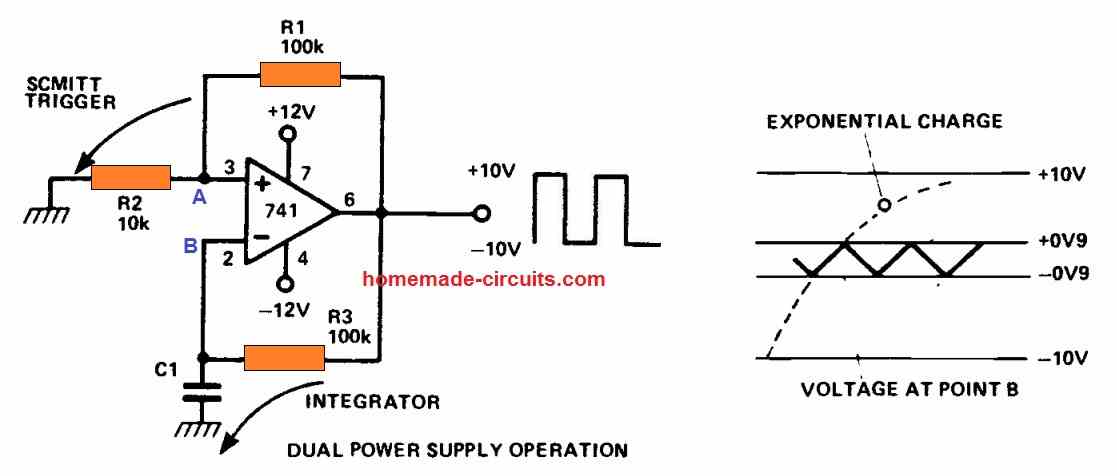
As a result, R3 discharges C1. Once the voltage on C1 falls below -0.9 V, the process is reversed, and the op amp output returns to its high state. As a result, the circuit oscillates, creating a square wave with a voltage range of +10V to -10y. The voltage fluctuations on C1 can be used to determine the working frequency of the op amp oscillator.
This is the collapsed portion of an exponential charge/discharge waveform, but we'll disregard it and pretend it's linear (which it almost is). The frequency may be calculated using the following formula:
F = I / ΔV x C
where I represents the charging current (about 100 A), ΔV represents the charge over C1 (3.6 V), and C represents the capacitance in Farads.
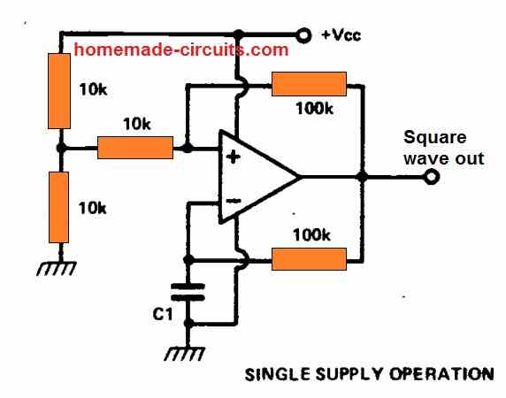
The above design uses a dual supply for the operation, for a single supply operation, we can apply the following configuration:
In the following paragraphs we will further learn about seven op amp IC oscillators, with three RC configurations, three LC configurations, and one crystal set up. These are very common op amp oscillator circuits which could be applied with pretty much any high-gain operational-amplifier IC.
Since any op amp can be used in these configurations, the precise pin numbers aren't specified, except from the standard pins like the inverting input, noninverting input, input ground (common), and output.
The voltage supply pinouts are not indicated, considering that these (Vcc and Vee pinouts) can change with the specific IC. Wherever feasible, the maximum functional working details is provided for all these basic configurations.
2) TWIN-T RC AF OSCILLATOR
The first figure below illustrates the a resistance-capacitance tuned AF op amp oscillator twin-T null network. This is implemented through the RC network of C1-C2-C3-R2-R3-R4, which decides the frequency level of the output.
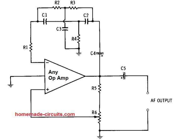
The op amp IC needs to have a voltage gain of 60 dB. This set up is basically an intensely tuned af amplifier on which a positive feedback is introduced so that it begins oscillating.
The twin-T network is introduced in the negative-feedback loop, and since it works like a null network it helps in eliminating a particular frequency (fr) through the negative feedback. The IC gain gets terminated appropriately at all other frequencies, while fr is conveniently transmitted forward. In this oscillator network, the following formulas can be used for the calculations:
- C1 = C2 = 1/2 C3
- R2 = R3 = 2R4
- fr = 1 / (2πR2C1)
In the above formula,
C's will be in farads,
R's will be in ohms,
and the unit of fr will be in hertz.
Coupling capacitor C4 blocks the DC current, and offers a high capacitance with respect to the capacitors C1, C2, and C3. It consequently doesn't have an effect on fr.
Resistor R1 offers a high resistance, based on the IC's input impedance, and helps to decrease loading of the twin-T network through the IC input circuit.
The inclusion of positive feedback, by means of the signal divider R5-R6, results in this very sharply tuned amplifier to oscillate with the frequency fr. When the potentiometer R6 is adjusted to the level where the circuit merely starts to oscillate, output-signal distortion is found to be minimal.
The op amp oscillator circuit could be made to work like a continuously tunable oscillator (e.g., from 20 Hz to 20 kHz) simply by replacing the resistors R2, R3, R4 with a 3-ganged potentiometer, and selecting capacitors C1, C2, and C3 in trios to adjust the bands.
Output control could be accomplished through a potentiometer which may be configured either to the output or introduced between stages of the IC.
3) PHASE-SHIFT RC AF OSCILLATOR
The phase-shift form of tuned resistance-capacitance audio frequency oscillator are popular for their extremely low harmonic distortion. In this form of oscillator, RC tuning is achieved through a 180-degree phase-shift network configured within the feedback loop of an inverting amplifier.
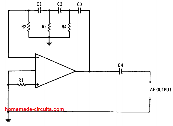
The network consequently generates the precise signal phase rotation for the oscillation. Fig. 2 above demonstrates the configuration for a phase-shift-type IC oscillator. In this set up, the phase shift network includes 3 RC legs in cascade pattern which are identical to each other: C1-R2, C2-R3, and C3-R4.
In this network , C1 = C2 = C3, and R2 = R3 = R4. All of these legs brings about a 60 degrees of phase shift. The frequency level where the entire shift gets to 180 degrees can be determined through the below given formula:
fr= 1/ (10.88R2C1)
To be able to offset the built in attenuation of the RC system, the op amp's gain must be around 40 dB. The op amp's noninverting input isn't utilized in this configuration, as it is delivered back to the ground by means of the resistor R1 ( which can be around 1000 ohms).
This op amp oscillator circuit could be turned into a continuously tunable type in the range of 20 Hz to 20 kHz, simply by replacing resistors R2, R3, R4, with a 3-gang potentiometer, and by switching the capacitors C1, C2, and C3 in trios, in order to select the bands.
But, the circuit's attenuation increases as the values of the resistances is reduced, and this situation could lead to the output-signal amplitude going down very fast with frequency, and oscillation may simply stop if R2, R3, and R4 are adjusted to lower values with the high frequencies.
Output control could be provided through a potentiometer which could be either connected to the output of the op amp oscillator circuit or introduced between the stages of the op amp.
4) WIEN-BRIDGE RC AF OSCILLATOR
We have so far learned that the resistance-capacitance-tuned audio frequency oscillators involve 3 resistances and 3 capacitances for the tuning process. However, the op amp oscillator circuit displayed in Fig. 3 below requires just a couple of resistances (R1 and R2) and a pair of capacitances (C1 and C2) for the same tuning facility.
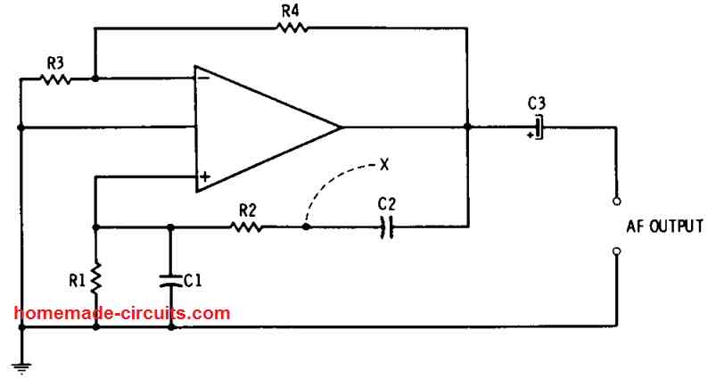
The C1-C2-R1-R2 network forms the 50 % of a Wien bridge network which, just like the twin-T network in Fig. 3-1, is sensitive to the frequency. The RC configuration is attached inside the positive-feedback link (on the noninverting input terminal). In this configuration, C1= C2, R1 = R2, and the frequency response can be determined using the below given equation:
fr = 1 / (2πR1C1)
In the above equation,
fr will be in hertz,
R1 will be in ohms,
C1 will be in farads
The resistors R3, and R4 does the job of providing the negative feedback (that works like a a signal voltage divider) to the inverting input terminal. This negative feedback helps to reduce the output-signal distortion; but, it should be implemented with the right proportion (by appropriately adjusting R3 and R4). This is important to ensure that it doesn't terminate the positive feedback leading to the elimination of the oscillation.
This form of op amp oscillator circuits could be easily turned into a continuously tunable oscillator in the range of 20 Hz to 1 MHz, simply by replacing the resistors R1, and R2 with a dual-gang potentiometer, and by ensuring that the capacitors C1 and C2 are switched in pairs in order to adjust frequency bands.
The tuning of the oscillator circuit can be implemented over a large frequency range, but, its output-signal amplitude might show a varying tendency with response to the frequency.
Nevertheless this varying tendency of the amplitude could be decreased using an appropriately dimensioned nonlinear resistor, for instance a thermistor, varistor, or double-ended zener diode, hooked up in between point "X" and ground. Controlling the output of the oscillator can be executed through a potentiometer which may be either incorporated into the output or placed between the stages of the IC.
5) TRANSFORMER-FEEDBACK AF OSCILLATOR
Fig. 4 below displays the a basic af oscillator configuration where a small audio transformer (T1) is used for providing both the feedback and the tuning which forces the op amp to work like an oscillator. Any low-gain op amp IC could work effectively in this configuration.
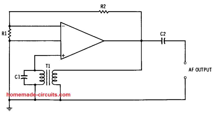
In this oscillator set up, transformer T1 provides the positive feedback to the non-inverting input of the op amp. T1 transformer can be any form of small transformer. The frequency of oscillation can be calculated through the capacitance C1 and the inductance (L) of the L1 transformer winding. The below given formulas can be used for the Fig. 3-4:
- C1 = 1 / (4π2F2L)
- L = 1 / (4π2F2C1)
- fr = 1 / (2π √LC1)
In the above formula,
fr is measured in hertz,
L is measured in henrys,
C1 is measured in farads
It is crucial to ensure that the connection of the transformer winding with the circuit is phased correctly for sustaining the oscillation. However if you find oscillations not working because of wrong transformer winding connections, you may need only one winding of the transformer to be reversed, that's all.
Resistors R1 and R2 do the job of applying the negative feedback, through a signal-voltage divider, to the inverting input terminal. This negative feedback helps to minimize output-signal distortion; but, this must be applied in a properly balanced manner (by suitably adjusting R1 and R2).
This is important to ensure that it doesn't suppress the positive feedback and as a result destroys the oscillation. The output can be controlled through a potentiometer which may be in two ways either to the output or placed between the IC stages.
6) TRANSFORMER-FEEDBACK RF OSCILLATOR
The radio-frequency or the RF oscillator circuit indicated below in Fig. 5 is identical to the transformer-feedback af oscillator explained in the previous section, except that in this particular rf oscillator, positive feedback for the oscillation and tuning are supplied through an air-core transformer, L1-L2. Any low-gain IC could work effectively in this circuit.
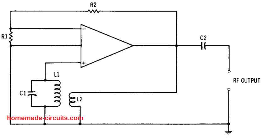
In this op amp oscillator circuit set up, the noninverting input of the op amp gets the positive feedback by means of the inductors L1-L2 together. (L1 can be the winding of the transformer that consists of higher number of turns, while L2 can approximately have one-quarter of the turns in L1. L2 winding needs to be wound closely to the L2 winding, however this coupling does not need to be tightly wound. The oscillation frequency fr can be calculated through the values of the capacitor C1 and the inductor L1.
This frequency fr can be determined through formulas as given below:
- C1 = 1 / (4π2F2L)
- L1 = 1 / (4π2F2C1)
- fr = 1 / (2π √L1C1)
In the above equation, the unit of C1 is picofarads, unit of L1 is in microhenrys, and the unit of fr is in megahertz.
It is crucial to connect the transformer winding with the right phasing in order to start the oscillation. That said, if you find the oscillations not happening, because of a wrong winding connection, you would only require just one winding ends to be reversed, that's all.
R1 and R2 performs the role of applying the negative feedback to the inverting input terminal of the op amp, by forming a signal-voltage divider. This negative feedback helps to stabilizes the working of the op amp oscillator and minimizes the output-signal distortion.
But, this negative feedback needs to be correctly balanced by appropriately adjusting the values of R1 and R2. This is important to ensure that it doesn't terminate the positive feedback and in the course destroys the oscillation.
The variable capacitor C1 can be used for getting a continuous tuning of the oscillator. In order to get a larger range of adjustment, L1 and L2 could be modified as pairs for selecting the frequency bands.
7) USING AF/RF OSCILLATOR TOGETHER
The Fig. 6 shown below exhibits an oscillator configuration that, which uses plug-in type inductors and capacitors, for producing both audio-frequency or radio-frequency signals through a diverse range of frequency.
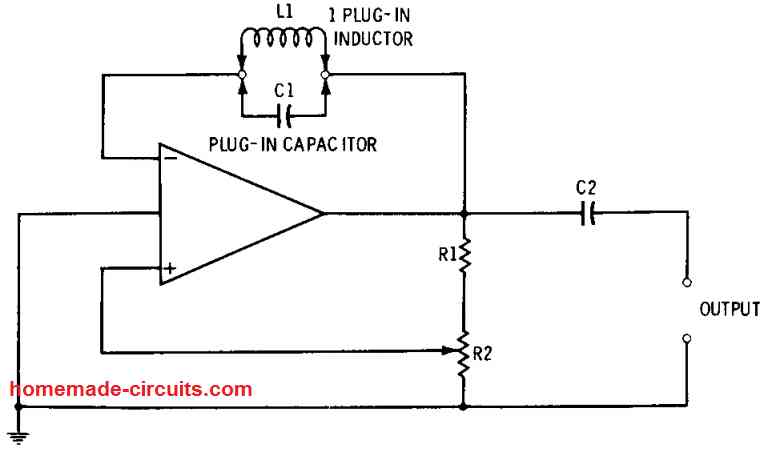
In this op amp oscillator set up, the positive and negative feedback are used both together. The tuned circuit built using the L1, C1 parts connected in the negative-feedback loop decides the oscillation frequency of the circuit. Since the L1, C1 works like a wavetrap, this tuned stage of the circuit eliminates its resonant frequency, fr, from the feedback loop.
The op amp consequently behaves like a sharply tuned amplifier, becomes responsible for transmitting the frequency fr. However, its gain gets terminated at all other frequencies. The positive feedback, provided by the resistors R1 and R2 which are configured like a signal voltage divider, subsequently enables the op amp to oscillate at frequency fr.
The parameters in this circuit can be calculated using the following given formulas:
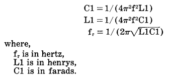
Using a high value capacitance and inductance together enables the generation of audio frequencies, whereas using lower values of capacitance and inductance enables the production of radio frequencies.
The strength at which the oscillation takes place is determined by the the adjustment of positive-feedback potentiometer R2. Therefore the R2 allows controlling the level of output-signal amplitude. The circuit can work using a number of different op amps.
Considering that output-coupling capacitor C2 is required to generate both low and high frequencies, its value must be suitably adjusted to some intermediate value, for example it can be 0.01 µF, unless of course the user is prepared to change this capacitor in addition to L1 and C1.
8) CRYSTAL-CONTROLLED RF OSCILLATOR
The below given Fig. 7 demonstrates an op amp based a crystal-controlled RF oscillator circuit that can work without the need of any tuning. This configuration can operate with multistage op amp circuits with various sensitivity levels. Having said that,it is advised to make use of medium and high-gain op amps.
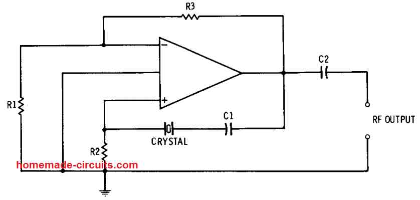
In this configuration, the crystal (XTAL) works like an exceptionally high-Q bandpass filter within the op amps's positive-feedback loop. The positive-feedback current transferred through the crystal, builds up a voltage drop around resistor R2, which is utilized on the op amp's noninverting input pin of the IC.
This finally forces the circuity to oscillate with the crystal frequency. Capacitor C1 is utilized simply for blocking the DC content, through a capacitance whose value specifically selected for low reactance at the crystal frequency.
The input ground of the op amp which is common ground is connected directly to the circuit ground, as indicated in the diagram. The circuit can be also seen having a negative-feedback loop, created using the resistors R1 and R3, which constitues a signal voltage divider network.
Negative-feedback current flowing by means of this resistive divider causes a voltage drop to appear across resistor R1, which is supplied to the op amp's inverting input pin.
It may be important to adjust the amplitude of this voltage by appropriately setting up the values of the resistors R1 and R3. This ensures that the positive feedback does not gets terminated, eventually killing the oscillation.
The use of the negative feedback helps to enhance stability of this op amp oscillator circuit and also helps to minimize the output-signal distortion. Nevertheless, this could be totally furnished only when a high harmonic output is needed, for example, in many of the transmitter type circuit applications.
9) Using MOS Op Amp
A MOSFET op-amp is configured as IC1. As a result, its input bias current is really very low, generally 10pA against 100nA for a 741. This enables the creation of circuit designs that use extremely little current. An integrator (IC1) and a Schmitt trigger are shown in the circuit (IC2).
Assume that the Schmitt's output is high (+10V). R4, R5 have a voltage of around +1V at their junction. This sends a 1uA current via R1, which enables the charging of C1.
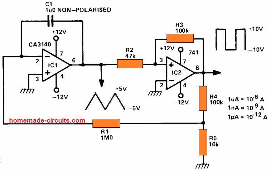
As a result, C1 (IC1's output) slopes down at the speed of 1/C, which in this example is 1V/sec. The Schmitt trigger switches to its low logic state when this voltage hits -5V. (-10y).
The current subsequently travels in the opposite direction via R1, and the output of IC1 ratchets up at 1V/sec. This process repeats until the voltage hits +5V. (the upper hysteresis magnitude of the Schmitt).
The Schmitt trigger then leaps to its highest output, repeating the period procedure. A square wave (10V) and a triangle (5V) are generated by the circuit. The time interval is 20 using the parts indicated. Set R1 = 10M for 200 seconds, and R1 = 10M, R5 = 1R for 2000 seconds.
10) Low Frequency IC 741 Oscillator
Using only a 741 operational amplifier as a comparator, this circuit generates a low-frequency square wave. The frequency may be changed by altering the values of C1 (10u) and R4 (10k). A decrease in C1 or R4 raises the frequency, whereas an increase in value lowers it.
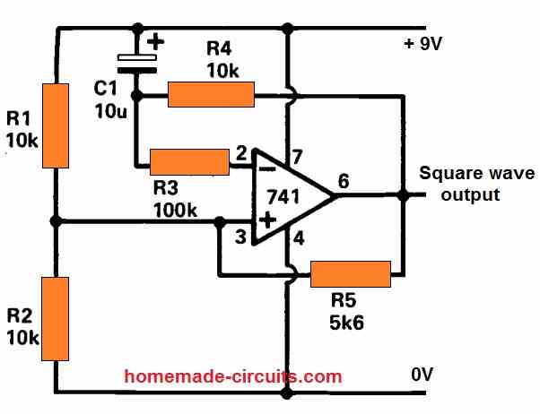
Imagine that the 741's output is low initially, to demonstrate how the circuit works. The inverting input would be at a supply level that is less than half. Assuming that C1 is also uncharged. Due to the current flowing via R4, the bottom end of C1 will begin to drop in voltage until it reaches the value at pin 3. In this situation, t he output of the 741 (which compares voltages at pins 2 and 3) will turn positive. C1 will repeat the process when the voltage at pin 3 rises to the other side of half supply, forcing the 741 output to follow and generate a squarewave.
Op amp Oscillator, Formulas, and Design Considerations
An oscillator build using an op amp as the active element is called an op amp oscillator.
In the following paragraphs I have explained how to design op amp based oscillators, and regarding the many critical factors required for generating a stable oscillator design.
Op amp based oscillators are normally used to generate precise, periodic waveforms like square, sawtooth, triangular, and sinusoidal.
Generally they operate using a single active device, or a lamp, or a crystal, and associated by a few passive devices like resistors, capacitors, and inductors, to generate the output.
Op-amp Oscillator Categories
You will find a couple of primary groups of oscillators: relaxation and sinusoidal.
Relaxation oscillators produce the triangular, sawtooth and other nonsinuoidal waveforms.
Sinusoidal oscillators incorporate op-amps using additional parts accustomed to create oscillation, or crystals which have in-built oscillation generators.
Sine wave oscillators are employed as sources or test waveforms in numerous circuit applications.
A pure sinusoidal oscillator features solely an individual or basic frequency: ideally without any harmonics.
As a result, a sinusoidal wave could be the input to a circuit, using calculated output harmonics to fix the level of distortion.
The waveforms in relaxation oscillators are produced through sinusoidal waves which are summed to deliver the stipulated shape.
Oscillators are helpful for producing consistent impulses which are used as a reference in applications like audio, function generators, digital systems, and communication systems.
Sine Wave Oscillators
Sinusoidal oscillators comprise op-amps using RC or LC circuits that contain adjustable oscillation frequencies, or crystals that possess a predetermined oscillation frequency.
The frequency and amplitude of oscillation are established by the selection of passive and active parts hooked up with the central op-amp.
Op-amp based oscillators are circuits created to be unstable. Not the type which are at times unexpectedly developed or designed in the lab, rather types that are deliberately built to be in an unstable or oscillatory condition.
Op-amp oscillators are tied to the bottom end of the frequency range due to the fact op amps lack the necessary bandwidth for implementing the low phase shift at high frequencies.
Voltage-feedback op amps are restricted to a low kHz range since their principal, open-loop pole is often as small as 10 Hz.
The modern current-feedback opamps are designed with significantly broader bandwidth, but these are incredibly difficult to implement in oscillator circuits as they are sensitive to feedback capacitance.
Crystal oscillators are recommended in high-frequency applications in the range of hundreds of MHz range.
Basic Requirements
In the most basic type, also called the canonical type a negative feedback method is used.
This becomes the prerequisite for initiating the oscillation as shown in Figure 1. Here we see the block diagram for such a method wherein VIN is fixed as the input voltage.
Vout signifies the output from the block A.
β denotes the signal, also called the feedback factor, which is supplied back to the summing junction.
E signifies the error element equivalent to the sum of the feedback factor and the input voltage.

The resulting equations for an oscillator circuit can be seen below. The first equation is the important one which defines the output voltage. Equation 2 gives the error factor.
Vout = E x A ------------------------------(1)
E = Vin + βVout --------------------------(2)
Eliminating the error factor E from the above equations gives
Vout / A = Vin - βVout ----------------- (3)
Extracting the elements in Vout gives
Vin = Vout (1/A + β) ---------------------(4)
Reorganizing the terms in the above equation provides us the following classical feedback formula through equation #5
Vout / Vin = A / (1+Aβ) ----------------(5)
Oscillators are able to work without the help of an external signal. Rather, a portion of the output pulse is utilized as the input through a feeedback network.
An oscillation is initiated when the feedback fails to achieve a stable steady state. This happens because the transfer action does not get fulfilled.
This unstability occurs when the denominator of equation #5 becomes zero, as shown below:
1 + Aβ = 0, or Aβ = -1.
The crucial thing while designing an oscillator circuit is to ensure Aβ = -1. This condition is called the Barkhausen criterion.
To satisfy this condition, it becomes essential that the loop gain value remains at unity through a corresponding 180 degrees phase shift. This is comprehended by the negative sign in the equation.
The above results can be alternatively expressed as shown below using symbols from complex Algebra:
Aβ = 1ㄥ-180°
While designing a positive feedback oscillator the above equation can be written as:
Aβ = 1ㄥ0° which makes the term Aβ in equation #5 negative.
When Aβ = -1 the feedback output tends to move towards an infinite voltage.
When this approaches the maximum + or - supply levels, the gain level active devices in the circuits changes.
This causes the value of A to become Aβ ≠ -1, slowing down the feedback infinite voltage approach, eventually putting it to a halt.
Here.we may find one of the three possibilities happening:
- Non-linear saturation or cut-off causing the oscillator to stabilize and lock.
- The initial charge forcing the system to saturate for a much long period before it again becomes linear and begins approaching the opposite supply rail.
- The system continues to be in the linear region, and reverts towards the opposite supply rail.
In case of the second possibility, we get an immensely distorted oscillations, generally in the form of quasi square waves.
What's Phase shift in oscillators
The 180° phase shift in the equation Aβ = 1ㄥ-180° is created through the active and passive components.
Just like any correctly designed feedback circuit, oscillators are built based on the phase shift of the passive components.
This is because the results from passive parts are precise and practically drift-free. The phase shift acquired from active components is mostly inaccurate due to many factors.
It may drift with temperature changes, may show wide initial tolerance, and also the results could be dependent on the device characteristic.
Op amps are chosen in order to ensure that they bring about minimum phase shift to the frequency of the oscillation.
A single pole RL (resistor-inductor) or RC (resistor-caapcitor) circuit brings about approximately 90° phase shift per pole.
Since 180° is necessary for oscillation, a minimum of two poles are employed while designing an oscillator.
An LC circuit possesses 2 poles; therefore, it provides around 180° phase shift for each pole pair.
However we won't be discussing LC based designs here due to the involvemenet of low frequency inductors that can be expensive, bulky, and undesirable.
LC oscillators are intended for high-frequency applications, that may be over and above the frequency range of opamps based on voltage feedback principle.
Here you may find the inductor size, weight, and cost are not of much importance.
Phase shift ascertains the frequency of oscillation since the circuit pulses at the frequency that fetches a phase shift of 180 degress. The df/dt or the rate at which the phase shift changes with frequency, decides frequency stability.
When cascaded buffered RC sections are used in the form of opamps, offering high input and low-output impedance, the phase shift multiplies by the number of sections, n (see Figure below).
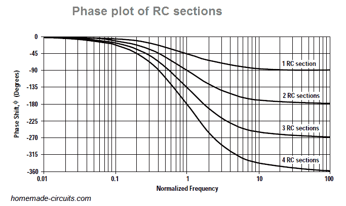
Despite the fact that two cascaded RC sections present 180° phase shift, you may find dФ/dt to be minimal at the oscillator frequency.
As a result oscillators constructed using two cascaded RC sections offer inadequate frequency stability.
Three identical cascaded RC filter sections provide an increased dФ/dt, enabling the oscillator with an enhanced frequency stability.
However, introducing a fourth RC section creates an oscillator with an outstanding dФ/dt.
Hence this becomes an extremely stable oscillator setup.
Four sections happen to be the preferred range mainly because opamps are available in quad packages.
Also, the four-section oscillator produces 4 sine waves which are 45° phase shifted with reference to one another, which means this oscillator enables you to get hold of sine/cosine or quadrature sine waves.
Using Crystals and Ceramic Resonators
Crystal or ceramic resonators provide us with the most stable oscillators. This is because resonators come with an incredibly high dФ/dt as a result of their nonlinear properties.
Resonators are applied in high-frequency oscillators, however, low-frequency oscillators usually do not work with resonators due to size, weight, and cost constraints.
You will find that op-amps are not utilized with ceramic resonator oscillators mainly because opamps include a reduced bandwidth.
Studies show that it is less expensive to construct a high-frequency crystal oscillator and trim down the output to acquire a low frequency instead of incorporating a low-frequency resonator.
Gain in oscillators
The gain of an oscillator must match one at the oscillation frequency. The design gets steady once the gain is greater than 1 and oscillations halt.
As soon as the gain reaches over 1 along with a phase shift of –180°, the non linear property of the active device(opamp) drops the gain to 1.
When non-linearity occurs the opamp swings near the either (+/-) supply levels due to the reduction in the cut-off or saturation of the the active device (transistor) gain.
One strange thing is that the badly designed circuits actually demand marginal gains in excess of 1 during their production.
On the other hand, higher gain leads to greater amount of distortion for the output sine wave.
In cases where gain is minimal, oscillations cease under extreme unfavorable circumstances.
When the gain is very high, the output waveform appears to be much more similar to a square wave instead of a sine wave.
Distortion is usually an immediate consequence of too much gain over-driving the amplifier.
Therefore, gain should be cautiously governed for for achieving low distortion oscillators.
Phase-shift oscillators can show distortions, however they may have the ability to attain a low-distortion output voltages using buffered cascaded RC sections.
This is because cascaded RC sections behave as distortion filters. Furthermore, buffered phase-shift oscillators experience low distortion since the gain is managed and uniformly balanced between the buffers.
Conclusion
From the above discussion I have explained the basic working principle of opamp oscillators and understood regarding the fundamental criteria for achieving sustained oscillations. In the next post we'll learn about Wien-bridge oscillators.
i In #7 you show a tank circuit. Assume a 741 op-amp. What R1 and R2 do you suggest to start with? I realize that these might be varied, according to the L/C tank requirements.
You can try 100K for R1 and R2. Yes, the values are related to the LC tank circuit and can be varied.
Call me a lazy one but what would the equation be for picking capacitors to fall within a particular range? Say I wanted the 20Hz to 20kHz bandwidth, what equation would equal the 20Hz to 20KHz frequency range? Feel free to ignore if i am asking too much. I am curious though of the equation.
That’s a valid question, I think that could be only identified through a practical testing, with the help of a frequency meter.
valid but wasn’t clear i was referring to the first circuit for someone else reading. But thank you for your response!