In this post I have explained a variety of op amp preamplifier circuits, and there should be an appropriate layout here for almost any standard audio preamplifier application.
As the name suggests itself, a preamplifier is an audio circuit which is used before a power amplifier, or between a small signal source and a power amplifier.
The job of a preamplifier is to raise the level of the small signal to a reasonable level so that it becomes suitable for the power amplifier for further amplification into a loudspeaker.
Contributed by: Matrix
Microphone Preamp
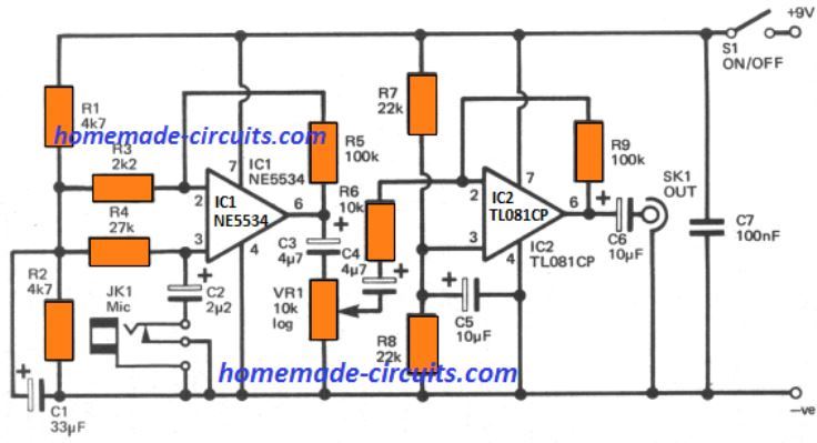
The microphone preamplifier shown above features a voltage gain of over 52dB (400 times) which could suit a high impedance dynamic or electret microphone to just about any section of an audio gear.
If employed in association with standard microphones as mentioned here, an output of approximately 1 volt RMS could be easily obtained, although a gain control makes it possible for a lower output to be set to ensure that overloading of the circuit by the load could be eliminated.
The signal to noise ratio of the circuit is outstanding and is normally above 70 dB with respect to an output of 1 V RMS (with full gain and unloaded).
How it Works
The proposed op amp MIC preamplifier circuit consists of a couple of stages, which includes IC1 as the non-inverting amplifier. and IC2 as an inverting amplifier.
Each amplifiers are commonly available types. IC1's closed loop gain is fixed at around 45 times through a negative feedback circuit built using the R3 and R5 network.
The circuit's input impedance is fixed at a minimal value of 27k by means of R4, which is sufficient to make sure that extreme loading of the microphone doesn't happen, C2 enables DC blocking at the circuit input.
The circuit also has a network of parts connected with the input jack that removes any kind of stray electrical noise pick up and additionally inhibits probable oscillation caused by spurious feedback.
The device employed for IC1 is a NESS34 or NE5534A which is actually a high end operational amplifier. The NE5534A is marginally superior to the IC NE5534 although the two ICs provide exceptional functionality using minimal noise and distortion figures.
C3 is used as a coupling capacitor across the output of IC1 and VR1. VR1 acts like a normal pot gain control.
Next, the signal is coupled to the following amplification stage. Resistors R6 and R9 constitute a negative feedback network which ensures a closed loop voltage gain of 10 to IC2.
This enables the circuit to achieve an overall voltage gain of around 450.
With regards to noise efficiency, extreme high performance is not critical here, and therefore any suitable op amp in place of IC2 will work.
Here we have used a TL081CP op amp, however, any other type such as the LF351 would also work as good. These types being a BiFET op amps provides extremely low magnitudes of distortions.
PCB Design

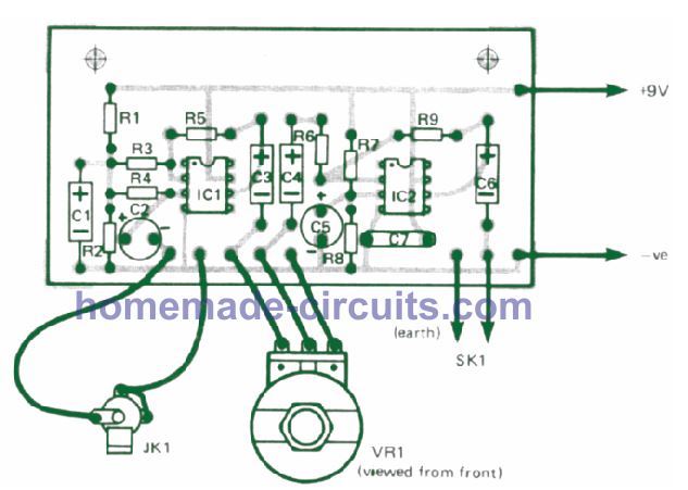
Component Layout
Universal Preamplifier using Op amp LM382
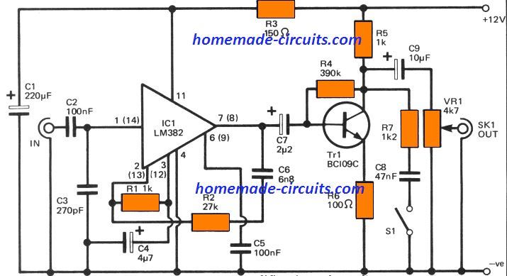
The circuit diagram below shows a basic universal audio preamp using the IC LM382, which offers very low noise, low distortion, and reasonably high gain, and this circuit can be used for practically all normal audio pre-amplifier circuit applications.
How it Works
The resistors R2 and the capacitor C6 enable equalization, which can be seen between the preamplifier output and inverting input.
At low frequencies C6 includes a high impedance resulting in low feedback frequency and high voltage gain.
At larger frequencies the impedance of C6 slowly decreases, providing enhanced negative feedback and rolling off the circuit response at the necessary 6dB per octave.
It only extends up to a frequency of around 2kHz, because above it frequency the impedance of C6 is quite small compared with that of R2, which has no influence on the circuit 's degree of feedback or voltage gain.
R1 and C4 are a part of the feedback system as well. C2 is the input DC blocking capacitor and C3 is an RF filter condenser that helps to prevent RF interference and instability issues due to stray signals from the source to the non-inverting input (to which the input signal is coupled).
The LM382 does have a high level of output ripple exclusion, however due to its lower input signal level and the likelihood that noise fluctuations may be added to the supply lines.
Even though IC1 creates a significant amount of voltage gain, somehow it provides somewhere between 50mV RMS output level, which is around one tenth of the drive voltage needed by majority of hi-fr amplifiers.
Therefore Tr1 is incorporated in the form a a common emitter amplifier with a voltage gain of maybe 20dB.
R4 allows a constructive feedback that decreases Tr1's voltage gain to the right level, that additionally provides a lower degree of distortion. IC9 links Tr1 output to VR1 attenuator for getting an adjustable output.
Frequency Response
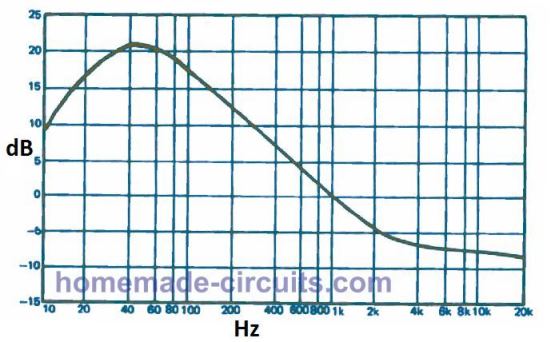
For unfiltered signals, a small quantity of noise reduction could be accomplished, essentially by using a treble cut filter, and a relatively smooth average frequency response can be obtained.
The process is implemented by applying treble boost however the quantity of boost adapted relies on the dynamic level of the signal.
It is highest throughout low-signal intervals and decreases to zero at the maximum with dynamic level signals.
When a music signal is applied at the input, the circuit enables a treble cut which again is optimized dynamically, this actually occurs in order to compensate a high treble boost response.
The universal pre-amplifier circuit has a top cut filter using R7 and c8, which allows an attenuation of around 5 dB with 10 kHz frequencies.
Due to this the high frequencies can be boosted by a magnitude of 5 dB for high signal levels. For medium signal inputs, the frequency response offered by the design is just flat.
Guitar Preamplifier Circuit
The basic function of this guitar pre-amplifier circuit is to integrate with any standard electric guitar and raise its low input string signals into a reasonably high pre-amplified signals which could be then fed to a bigger power amplifier for the desired boosted output
The output signal frequency from guitar pick-ups tends to differ greatly from pick-up to pick-up, and although some have a very high voltage that can push almost any power amplifier, some have just around 30 millivolts of RMS or so voltage.
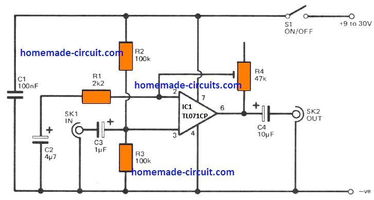
Amplifiers expressly built that can be used with guitars usually have a relatively high sensitivity and these could be used reliably for just about any pick-up, however when using a guitar with some other form of amplifier (such as a hi-fl amplifier) the overall volume achieved is always considered to be insufficient.
A easy remedy to this issue is to use a preamplifier as shown above, before feeding it to the power amplifier to raise the signal frequency amplitude.
The basic configuration mentioned here has a voltage gain that could really vary from unit to more than 26dB (20 times), therefore it should suit virtually every guitar pick-up to practically every power amplifier.
The preamplifier's input impedance should be about 50k, and the output impedance is low.
Therefore the circuit could be employed as a basic buffer amplifier with unity voltage gain to suit the fairly high output impedance of a guitar pick-up to a power amplifier having a low input impedance if required.
A solitary low-noise BIFET operational amplifier (IC1) has been used as a basis for the unit, which therefore has marginal distortion levels as well as a signal-to-noise ratio of around -70dB or higher even when the unit orksw with a very low output instrument like a guitar.
How it Works
This design is actually a normal operational amplifier non-inverting configuration circuit with R2 and R3 employed to bias the non-inverting IC1 input at around 50% of the supply voltage.
These likewise set the circuit's input impedance at approximately 50k. R1 and R4 form the network with negative feedback, also with R4 at minimum value 1C1 inverting control signals are directly coupled to each other, and the circuit provides unit voltage gain.
As R4 is calibrated for higher resistance the AC voltage gain decreases gradually, however C2 introduces DC blocking such that the DC voltage gain stays variable, and the amplifier 's output stays biased at @ ½ the supply voltage.
The amplifier's voltage gain is roughly equivalent to R1 + R4, divided by R1, resulting in a nominal overall voltage gain of maybe above 22 times with R4 at highest value.
The circuit's current consumption is around 2 milliamps through a 9 volt supply, which increases to approximately 2.5 milliamps when a 30 volt supply is used.
An effective voltage supply for the device is a compact 9 volt battery like a PP3 type. When a 9 volt supply is used, the average unclipped output voltage is around 2 volts RMS, and this works pretty much fine.
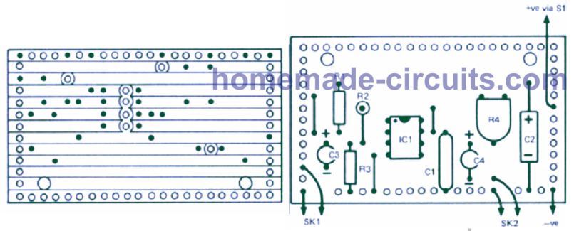
Strip Board PCB Connection Details and Components Layout Diagram
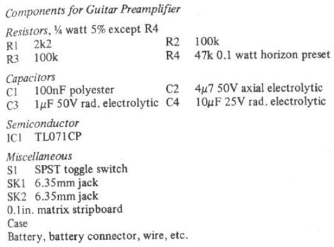
Parts List
High Impedance Buffer Amplifier
A buffer amplifier also works like an ideal pre-amplifier for most applications, however along with pre-amplification it also functions like a high impedance buffer between the signal input stage and the power amplifier stage.
This especially allows these types of preamplifiers to be used with extremely low current input signals, which cannot afford loading with other low impedance type preamps.
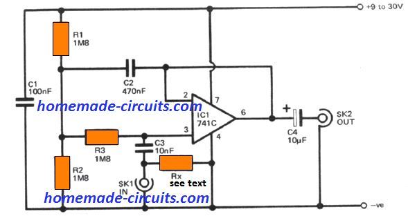
The buffer amplifier illustrated here has a normally more than 100 M input impedance at 1kHz, and the input impedance could be simply adjusted to just about any acceptable level below that point. The circuit's voltage gain is unity.
How it Works
Figure above displays the High Impedance Buffer Amplifier's circuit diagram, and the unit is essentially just an operating amplifier worked as a non-inverting amplifier for unity gain.
By coupling the output of IC1 directly to its inverting input, 100 per cent negative feedback is added over the system to achieve the unit voltage gain necessary along with a very high input impedance.
That being said, the bias circuit, which in this situation includes of R1 to R3, shunts the amplifier's input impedance so that the circuit overall provides an input impedance much smaller than IC1 alone. The input impedance is around 2.7 megohms, and for majority of the applications, this may be sufficient.
However, the shunting action of the bias resistors could be removed, and this is the objective of the C2 capacitor "bootstrapping." It connects the output signal to the three bias resistors junction, and thus any adjustment in input voltage is balanced by an equal voltage shift at the output of IC1 and at the intersection of the three bias resistors.
In the IC1 role, a basic 741 C operational amplifier is employed, and as stated previously, this provides an input impedance usually exceeding 100 megohms at 1 kHz that should be quite adequate for any standard implementation.
The higher input impedance that may be achieved using an operating amplifier for FET inputs really isn't of any practical importance, so there are a few drawbacks with most FET input systems in this circuit.
First that they actually have a propensity to oscillate when the input is open (when the input is attached to the device, the oscillations are attenuated and eliminated).
The other drawback is that the input power of so many FET input devices is substantially higher than bipolar devices like the 741 IC. Through this shunting actions, at most frequencies the input impedance is now reduced while at low bass and middle frequencies, the input impedance is simply higher.
For this purpose, a relatively low input impedance (like the pickup which has a recommended charge impedance of many 100 k ohm and M ohm is necessary), one way of achieving this is to eliminate C2 and change the quantities of R1 to R3 to achieve a desired input impedance.
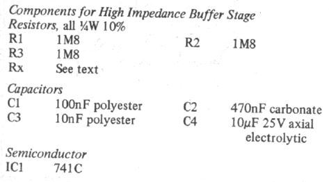
Parts List
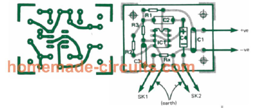
PCB Layout
Op Amp Preamplifier for 2.5 mV Signals
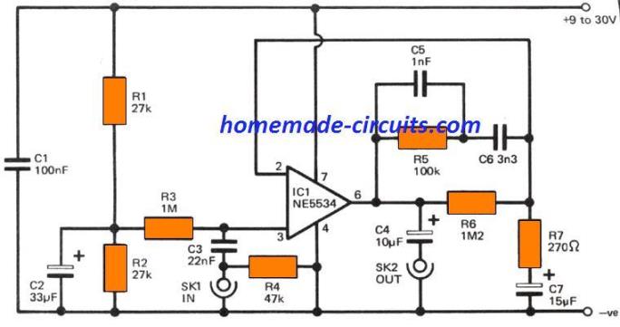
This particular op amp preamplifier circuit is extremely sensitive and will allow you to boost signals as low as 2.5 mV to a 100 mV. It is actually derived from an old RIAA preamplifier concept.
In earlier days, the output of a moving coil cartridge of a magnet or high voltage was typically 2.5 to 10 millivolt range, so that the pickup could be balanced with the power amplifier (this would possibly require an output signal of a couple of hundred millivolts RMS).
Although the output of magnetic and moving coil cartridges would rise at 6dB per octave it could do without the need of any equalization to counteract this since suitable equalization had to be involved during the recording process.
Nevertheless, equalization would be still necessary because during the recording process bass cut and treble boost would be used, in addition to adjusting, the frequency response often counteracted with a 6dB octave increase in pick-up output.
The bass cut had to be included to stop unnecessarily low-frequency groove modulations and the triple boost (with triple cut in playback) would provide a simple but efficient noise reduction facility.
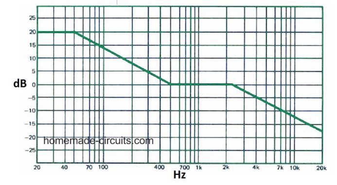
Figure above is actually a typical old RIAA preamplifier circuit's frequency response graph which shows the necessary parameters required for successfully implementing a highly sensitive preamplifier such as this.
How the Circuit Works
In real use RIAA equalization amplifiers typically would deviate a little from the perfect response, though device specifications weren't considered critically.
Actually, however even a straightforward equalization network made up of six resistance-capacitor sets typically results in a maximum error of not more than one or 2 dBs, which is actually looks quite OK.
R2, R3 used to link this distortion voltage to IC1. R2. C2 filters out any distortion or hum on the power supply, preventing the interference from being added to the amplifier feed.
The high R3 value provides a high input impedance for the circuit however, this is transferred by R4 to the necessary level of approximately 47k.
A few other pick-ups may present a load barrier of 100k and therefore R4 should be increased to 100k if the unit is to be implemented through an input signal as like we have in old pick-ups.
The high input impedance of the amplifier allows a very small part value to be employed for C3 without sacrificing the circuit's bass response.
It is advantageous because it eliminates a significant level of current surge from input pick-up signals switch ON, as soon as this device takes on its normal functioning process.
A frequency selective negative feedback over IC1 provides the necessary adjustment of the frequency response.
At mid-frequencies R5 and R7 are the main determinants of the circuit gain, but at lower-frequency frequencies C6 adds a substantial impedance of R5 to minimize negative feedback and boost the gain required.
Likewise, the impedance of C5 is small at high frequencies compared to the impedance of R5, and the impact of C5 shunting leads to greater feedback and the high frequency roll-off necessary.
Since the circuit generates a voltages gain of over 50db in mid audio frequencies, the output becomes sufficiently high to run any standard power amplifier even when it is used with an input signal of only about 2.5 mV RMS.
The circuit is powered from any voltage between approximately 9 and 30 volts, but it is advised to work with a reasonably high supply potential (approximately 20-30 volts) to enable a reasonable overload percentage.
When the circuit is applied with a high output signal but with only roughly 9 volt supply voltage, a small overload is likely to take place at the minimum.
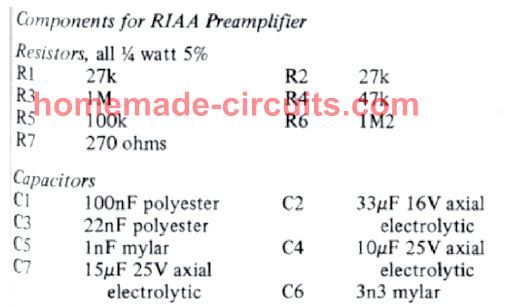
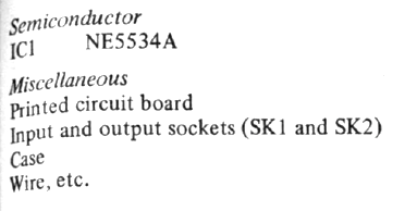
Parts List
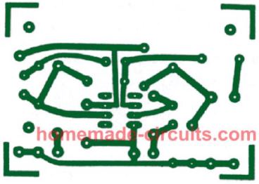
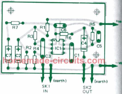
PCB Layout
Microphone preamplifier with High Stability
In audio gear preamplifiers, low noise factor should be accompanied with a variable gain feature.
Low-noise op amps usually do not, go well with low-impedance inputs for instance a dynamic microphone which is as a result is only popular with either input transformers or low-noise transistors with a feedback loop, a set up which often involve lack of stability along with significant disparities in gain setting.
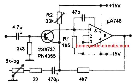
Overriding the input differential pair of the IC 748, as indicated, gets rid of potential instability.
The transistor is determined for any low noise attribute while driven from a 200 Ohm source, its collector current being variable for complementing exactly the same.
The high stability MIC circuit using just one op amp is exceptional due to its low noise, high stability and reduced distortion, despite the pretty simple dynamics of the circuit and having only a general-purpose op-amp. Resistor R2 is positioned for adjusting the symmetry of the circuit.
Phono Preamplifier Circuit using Op amp LM833
The cost-effective and high-performance LM833 operational amplifier, produced by National Semiconductors, serves as an exceptional choice for a phono signal input preamplifier.
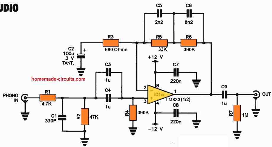
This circuit design is refreshingly uncomplicated, incorporating readily accessible components, and it boasts an impressively narrow RIM curve, maintaining a deviation within the range of plus or minus 2 dB from 30 Hz to 15 kHz.
With an input sensitivity of 3.2 mV and overload protection kicking in at 133 mV, it is well-suited for a wide range of applications.
For optimal performance, it is advisable to utilize all-metal film resistors with a 1% tolerance.
The capacitors should be of high quality and can either be metallized polyester (MKT) or polypropylene (MKP) types, rated at 50 volts.
To prevent the circuit from becoming overly bulky, expensive, or difficult to source, two 1uF capacitors are employed in parallel at the input. It's worth noting that C3 is a tantalum capacitor.
R1 and C1 play a crucial role in suppressing RF interference at the input, ensuring clean and reliable operation.