In this post I have explained the different methods of configuring a power factor correction circuit or a PFC circuit in SMPS designs, and explains the best practice options for these topologies so that it complies with the modern PFC restriction guidelines.
Designing efficient power supply circuits have never been easy, however in the course of time researchers have been able to solve most of the concerning issues, and quite in the same lines the modern SMPS designs are also being optimized with the best possible outcomes, thanks to the emerging regulatory standards which played an important role in implementing stricter quality parameters for the modern power supply units.
PFC Guidelines
The modern power supply quality restrictions are quite aggressively laid down, collectively by efforts of the manufacturers, suppliers and other concerned governing bodies.
Among the many quality parameters laid down for the modern power supply designs, power factor correction correction (PFC) which is actually in the form of harmonic cancellation has been declared as a mandatory requirement by the the IEC 61000-3-2 rules.
Due to this designers are forced to face tougher challenges in designing power factor correction stages in their power supply designs in order to meet these stringent modern laws, and with power supplies getting more and more formidable with its specs and application range, structuring proper PFC circuits is not getting any easier for the many manufacturer in the arena.
The presented tutorials are specially dedicated for all those associations and professionals who are into the manufacturing or designing of flyback SMPS for facilitating them with the most ideal PFC designs and calculations as per their individual requirements.
The discussions included in these tutorials will help you to design PFC circuits even for significantly large units in the range of upto 400 watts, 0.75 amps.
The readers will also get the opportunity to learn about selecting single-stage isolated converters which also includes LED drivers.The step by step design tutorial and instructions along with system level comparisons, the many designers actively involved in the power electronics field will be enlightened to go about with the most optimal approach for their specific application needs
Power Factor Correction Objective
Power factor correction circuit optimization within the modern SMPS (switch mode power supply) units could evolve in the recent past due to the advent of a number of advanced relevant integrated circuits (ICs), which has made possible to lay down different PFC designs having specific modes of operation and with individual challenge handling capability.
With the increase in the range of SMPS topologies the complexity in PFC designing and implementation has also aggravated in the present days.
In the first tutorial I have explained regarding the operational details of the design which is mostly preferred by the any professionals the corrections.
Basically, power factor correction helps to optimize the input current within off-line power supplies so that these are able to enhance the real power from the available mains input.
As per the normal requirement a given electrical appliance must emulate itself as a load having a pure resistivity, so that it enables it to have a zero reactive power consumption.
This condition results in the generation of almost zero input harmonic currents, in other words it allows the consumed current to be perfectly in line in phase with the input supply voltage which is normally in the form of a sine wave.
This achievement facilitates the appliance to consume the “real power” from the mains at the most optimal and efficient levels, which in turn results in minimizing wastage of electricity and increase its efficiency.
This effective use of electricity not only helps the appliance to present itself in the most efficient way but also for the utility companies and the involved capital equipment for the process.
The above feature furthermore enables the power lines to be free from harmonics and the resultant interference across the devices within the network.
Apart from the above mentioned advantages, including a PFC in modern power supply units is also for complying with the regulatory requirements as set in Europe and Japan with the IEC61000-3-2 which all electrical equipment should qualify.
The above mentioned condition has been regulated for most of the electronic appliances which may be rated at above 75 watt under Class D equipment standards or which are even higher, specifying the highest amplitude of the line-frequency harmonics ranging up to 39th harmonic.
Apart from these standards PFC is also employed for ensuring other efficiencies such as Energy Star 5.0 vital for computers, and Energy Star 2.0 for Power Supplies systems and TV sets since 2008.
Definition of Power Factor
PFC or Power factor Correction may be defined as the ratio of real power to apparent power, and expressed as:
PF = Real Power / Apparent Power, where Real Power is expressed in
Watts, while Apparent Power isexpressed in VA.
In this expression the real power is determined as the average of the instantaneous product of current and voltage across a phase or cycle, while the apparent power is deemed as the RMS value of current times the voltage.
This suggests that whenever current and voltage counterparts are sinusoidal and in phase with each other, the resultant power factor is 1.0.
However, in a condition when the current, voltage parameters are sinusoidal but not in phase, gives rise to a power factor that’s cosine of the phase angle.
The power factor conditions described above applies in cases where the voltage and current both are pure sine waves, in conjunction with a situation where the accompanying load is made up of resistive, inductive and capacitive components which may be all non-linear in nature, that is not adjusting with input current and voltage parameters.
SMPS topologies typically introduce non-linear impedance into the mains line due to the above explained natre of its circuitry.
How SMPS Works
An SMPS circuit basically includes a rectifier stage at the input which could be a half wave or a full wave rectifier and a complementing filter capacitor for holding the rectified voltage across it to the peak level of the input supply sine wave until the time the next peak sine wave appears and repeats the charging cycle of this capacitor, resulting in the required peak constant voltage across it.
This process of charging the capacitor on each peak cycle of the AC demands that the input must be equipped with enough current for fulfilling the load consumption of the SMPS, in between these peak intervals.
The cycle is implemented by dumping a large current into the capacitor quickly, which is applied to the load by through discharging until the next peak cycle arrives.
For this uneven charge and discharge pattern it’s a recommended that the pulse current from the capacitor is rated 15% higher than the average requirement of the load.
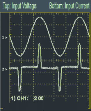
We can see in the above figure that despite of the significant amount of distortion the voltage and the current parameters are apparently in phase with each other.
However if we apply the “phase angle cosine” term to the above would give rise to an incorrect inference regarding the power supply being having a power factor of 1.0
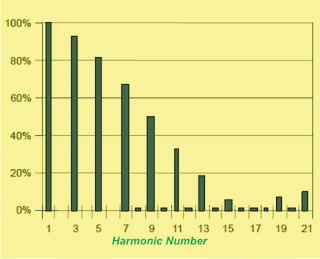
The upper and the lower waveforms indicate the amount of harmonic content of the current.
Here the “fundamental harmonic content” is indicated in comparison with an amplitude of 100%, while the higher harmonics are presented as the supplementary percentages of the fundamental amplitude.
However since the real power is determined only by the fundamental component, while the other supplementary harmonics only represent the apparent power, the actual power factor may be quite under 1.0.
We call this deviation by the term distortion factor which is fundamentally responsible for giving rise to a non-unity power factor in SMPS units.
Expression for Real and Apparent Power
A general expression which addresses the connection between the real and the apparent power may be given as follows:

Where cosΦ forms the displacement factor emerging from the phase angle Φ between the current/voltage waveforms and cosΦ signifies the distortion factor.
Referring to the diagram below, we can witness a situation which shows a perfect power factor correction.
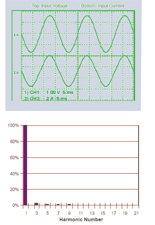
We can see that here the current waveform quite ideally replicates the voltage waveform as both are apparently running in phase and in sync with each other.
Therefore here the input current harmonics could be assumed to be almost zero.
Power Factor Correction Vs Harmonic Reduction
Looking at the earlier illustrations it’s evident that power factor and low harmonics work in sync with each other.
It is generally perceived that if limits for the respective harmonics are outlined might help to restrict the input current contamination in power lines by the way of eliminating interfering current disturbances with the other appliances in the vicinity.
Therefore while the processing of input current may be termed as “power factor correction” the output magnitude of refinement thought this processing is understood as harmonic content a per the international guidelines.
For SMPS topologies, it’s normally the displacement element which is approximately at unity, giving rise to the following relationships between power factor and harmonic distortion.

In the expression the THD represents the Total Harmonic Distortion as the quadratic sum of the harmful harmonics over the fundamental content, expressing the relative weight of the associated harmonic content with reference to the fundamental counterpart.The other equation associates the absolute figure of the THD and not in the % proportion, expressing that THD needs to be essentially zero in order to create a unity PF.
Types of Power Factor Correction
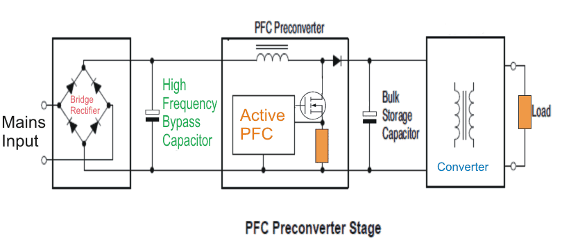
The input waveform characteristic in the above figure demonstrates a typical “active” type of power factor correction for an SMPS device introduced in between an input rectifier configuration and a filter capacitor, and through a PFC integrated circuit controlling the proceedings along with the associated circuitry for ensuring that the input current cohesively follows the input voltage waveform.
This type of processing may be considered as the most prevalent type of PFC employed in the modern SMPS circuits, as may be witnessed in the figure below.
Having said this, it is by no means mandatory that only “active” versions using ICs, and semiconductors be used for the proposed PFC, ll other form of design which may guarantee a reasonable amount PFC below the set regulations is normally welcomed.
It is been noticed that in fact a single inductor replacing the position of the “active” counterpart is able to quite satisfactorily reject the harmonics by controlling the peaks and by distributing the current uniformly in sync with the input voltage quite efficiently.
Passive PFC Design
However this form of passive PFC control could demand a significantly bulky iron cored inductor and therefore can be used for applications in which compactness is not the a crucial requirement. (page 12)
A passive single inductor could seem to be a quick solution for PFC but for high wattage application the size could begin getting uninteresting due to it’s impracticably large dimensions.
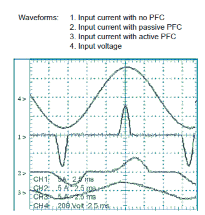
In the graph below we are able to witness the input characteristics of three numbers of 250 watt PC SMPS variants, each representing a current waveform at an equivalent scale factor.
We can easily see that the result obtained from a passive inductor based PFC is 33% higher current peaks, than with active PFC filter counterpart.
Even though this may be able to pass the IEC61000-3-2 standards, it will definitely not be on par with the recent more stringent 0.9PF requirement rule, and would fail the QC acceptance level, set as per this new standards.
Basic Block Diagram
Due to the ongoing electronic market trend where we can see copper costs on the rise along with the rise in the magnetic cores process and the introduction of modern, much cheaper semiconductor materials, it won’t be a surprise if we notice the active PFC approach getting exceedingly popular than the passive counterpart.
And this trend could be perceived to grow even stronger in the coming future, presenting more and more advanced and enhanced PFC solutions for the many SMPS designers and manufacturers.
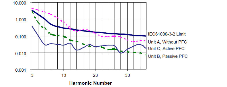
Comparing Input Line Harmonics to IEC610003-2 Standards
In Figure below we are able to see traces of three separate 250 watt PC SMPS results with reference to the IEC6000-3-2 restrictions. The indicated restriction is valid for all class D gadgets such as PCs, TVs, and their monitors.
The shown harmonic content limit are fixed in accordance to the input power of the devices. For products related to lights such LED lights, CFL lights, class C restrictions are normally followed, which are identically on par with their input wattage limits.
Other non-conventional electronic products find their PFC limit set in proportion to a minimum 600 watt input power.
If we look at the passive PFC trace we find it to be hardly in conformity with the set restriction limit, just a touch and go kind of situation (at harmonic no3)
Analyzing Passive PFC Features
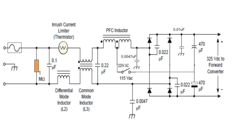
In the following figure we can see a classic example of passive PFC circuit designed for a traditional PC power supply. The notable thing here is the connection of center tap of the PFC inductor with the input line input voltage.
While in the 220V selection mode (switch open), the entire two sections of the inductor are applied with the rectifier network working like a full bridge rectifier circuit.
However in the 110V mode (switch close), just 50% or one half of the coil is utilized through the left side section of the coil being implemented whereas the rectifier section is now transformed into a half wave rectifier doubler circuit.
Since the 220V selection is bound to generate around 330V after full wave rectification, this forms the bus input for the SMPS and possesses the possibility of fluctuating significantly in accordance with the input line voltage.
Example Circuit Diagram
Although this passive PFC design might look quite simple and impressive with its performance it might exhibit a few notable drawbacks.
Along with the bulky nature of the PFC, two other things that affect its performance are first, the inclusion of a mechanical switch which makes the system vulnerable to a possible human error while operating the unit, and also the associated wear and tear issues.
Second, the line voltage being not stabilized results in relative inefficiencies in the fronts of cost effectiveness and DC to DC power conversion accuracy linked with the PFC output.
Critical Conduction Mode (CrM) Controllers
Controller stage called critical conduction mode which is also termed as transitional mode or borderline conduction mode (BCM) controller are circuits configurations which can be found effectively employed in lighting electronics applications. Although being hassle free with its usability, these controller are relatively expensive.
The following diagram 1-8 demonstrates a regular CrM controller circuit design.
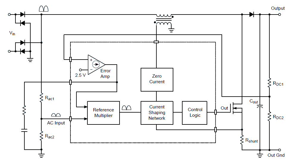
Typically a CrM controller PFC will possess the above shown kind of circuitry, which can be understood with the help of the following points:
An input of a reference multiplier stage receives an appropriately dimensioned signal from an associated error amplifier output having a low frequency pole.
The other input of the multiplier can be seen referenced with a stabilized DC clamped voltage extracted from a rectified AC line input.
Thus, the resultant output from the multiplier is the product of relative DC from the error amp output and the referenced signal in the form of full wave AC sine pulses from the AC input.
This output from the multiplier stage can be seen also in the form of full wave sine wave pulses but appropriately scaled down in proportion with the applied error signal (gain factor) use as the reference for the input voltage.
The signal amplitude of this source is appropriately tweaked in order to implement the right specified average power and to ensure a proper regulated output voltage.
The stage which is responsible for processing the current amplitude causes the current to flow in accordance with the output waveform from the multiplier, however the line frequency current signal amplitude (after smoothing) may be expected to be half that of this reference from the multiplier stage.
Here, the operations by current shaping circuitry may be understood as follows:
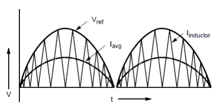
Referring to the diagram above, Vref stands for the signal out from the multiplier stage, which is further fed to one of the opamps of a comparator whose second input is referenced with the current waveform signal.
On power switch, the current across the inductor slowly increases until the signal across the shunt has reached the Vref level.
This forces the comparator to change its output from On to OFF switching OFF the power to the circuit.
As soon as this happens the voltage which was gradually ramping across the inductor begins to drop slowly towards zero and once it touches zero, the opamp output reverts and switches ON again, and the cycle goes on repeating.
As the name of the above characteristic signifies, the control pattern of the system never allows the inductor current to shoot above the predetermined limit across the continues and discontinuous switching modes.
This arrangement helps to predict and calculate the relationship between the average peak current level of the resultant output from the opamp. Since the response is in the form of triangular waves, the average of the waveform signifies precisely 50% of the actual peaks of the triangle waveforms.
This implies that the resultant average value of the current signal of the triangle waves would be = Inductor current x R sense or simply put half of the preset reference level (Vref) of the opamp.
The frequency of a regulators using the above principle will be dependent on the line voltage and the load current. The frequency could be much higher at higher line voltages and could vary as the line input varies.
Frequency Clamped Critical Conduction Mode (FCCrM)
Despite of its popularity in various industrial power supply PFC control applications, the above explained CrM controller involves some inherent drawbacks.
The main flaw of this type of active PFC control is its frequency instability with respect to line and load conditions, which shows an increase in frequency with lighter loads and higher line voltages, and also while each time the input sinewave approaches the zero crossings.
If an attempt is made to rectify this issue by adding a frequency clamp, results in an output with a distorted current waveform, which seems inevitable due to the fact that “Ton” remains unadjusted for this procedure.
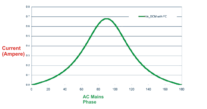
However the development of an alternative technique helps to achieve a true power factor correction even in the discontinuous mode (DCM). The principle of operation can be studied in Figure below and with the attached equations.
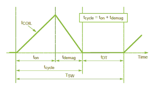
Referring to the diagram above, the coil peak current can be evaluated by solving:

The average coil current with reference to the switching cycle (which is additionally assumed as the instantaneous line current for the given switching cycle, owing to the fact that switching frequency is usually higher than the line frequency on which the variations of the line voltage takes place), is expressed with the formula:

Combining the above relationship and simplification of the terms gives the following:

The above expression clearly indicates and implies that in case a method is implemented wherein an algorithm takes care to maintain ton.tcycle / Tsw at a constant level, it would enable us to achieve a sinewave line current having a unity power factor even in the discontinuous mode of operation.
Although the above considerations reveals some distinct benefits for the proposed DCM controller technique, it’s doesn’t seem to be the ideal choice because of the associated high peak current levels, as demonstrated in the following table:
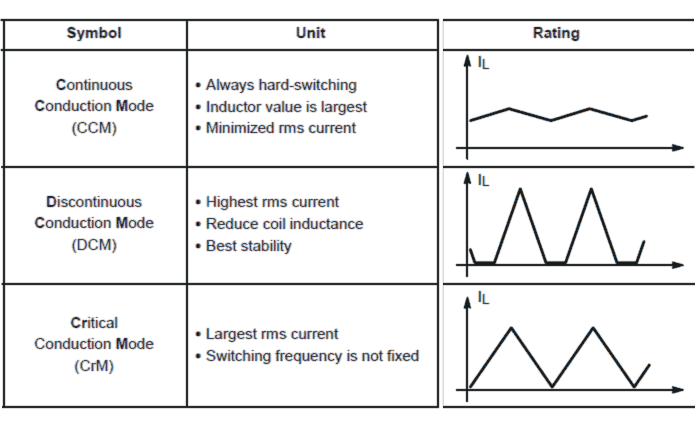
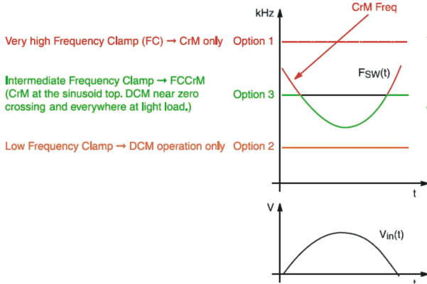
In order to achieve an ideal PFC conditions, a sensible approach would be to implement a condition where the DCM and the Crm modes of operations are merged for milking out the best out of these two counterparts.
Therefore when the load conditions are not heavy and the CrM runs at a high frequency, the circuit goes for a DCM mode of operation, and in case when the load current is high, the Crm condition is allowed to persist so that the current peaks do not tend to cross the undesirable high limits.
This kind of optimization across the two suggested control modes can be best visualized in the following figure where the benefits of the two control modes are merged for achieving the most desirable solutions.
Continues Conduction Mode
The continuous conduction mode of PFC could become quite popular in SMPS designs due to their their flexible application feature and range and the associated several advantages.
In this mode the current peak stress is maintained at a lower level resulting in minimized switching losses within the relevant components, and furthermore the input ripple is rendered at a minimal level with a relatively constant frequency, which in turn enables the smoothing process much simpler for the same.
The following attributes associated with CCM type of PFC needs to be discussed a bit more elaborately.
Vrms2 Control
One of the vital attributes with most PFC design universally applied is the reference signal which needs to be a steppe down imitation of the rectified input volage.
This minimized rectified equivalent of the input voltage is finally applied in the circuit for shaping the correct waveform for the output current.
As discussed above, a multiplier circuit stage is normally employed for this operation, but as we know that a multiplier circuit stage could be relatively less cost effective than a traditional twn-input multiplier system.
A classic example layout an be witnessed in Figure below which demonstrates a continuous mode PFC approach.
As can be seen, here the boost converter is triggered with the aid of an average current-mode PWM, which becomes responsible for dimensioning the inductor current (input current for the converter), with reference to the command current signal, V(i), which may be seen as the scaled down equivalent of the input voltage V(in) to a proportion of VDIV.
This is is implemented by dividing the error voltage signal with the square of the input voltage signal (smoothed by the capacitor Cf, in order to create a simplified scaling factor with reference to the input voltage level).
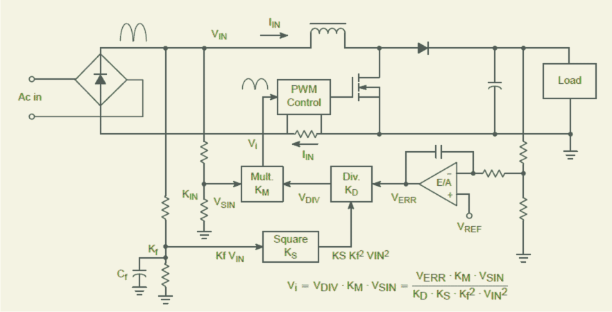
Although you may find it a bit awkward to see the error signal being divided by the square of the input voltage, the reason behind this measure is to create a loop gain (or a transient dependent response) which may not be based on the input voltage triggering.
The squaring of the voltage at the denominator neutralizes with the value of Vsin along with the transfer function of the PWM control (the proportionality of the current graph slope of the inducror with the input voltage).
However one downside of this form of PFC is the flexibility of the multiplier, which compels this stage to be a bit overdesigned especially the power handling sections of the circuit, so that it sustains even the worst-case power dissipation scenarios.
Average Current Mode Control
In the above figure we can see how the reference signal produced from the multiplier V(i) signifies the shape of the waveform, and the scaling range of the PFC input current .
The indicated PWM stage becomes responsible of ensuring an average input current to be on par with the reference value. The procedure is executed through an average current mode controller stage, as can be seen in the figure given below.
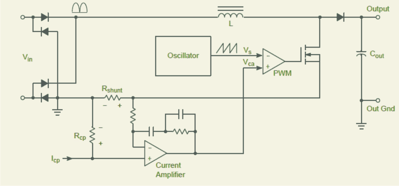
The average current mode control is basically configured to regulate the average current (input/output) with reference to the control signal Icp, which in turn is created by employing a low frequency DC loop through an error amplifier circuit stage, and this is nothing but the equivalent current corresponding to the signal Vi which is shown in the earlier figure to this.
The stage current amplifier functions as an current integrator as well as a error amplifier, in order to regulate the shape of the waveform, whereas the Icp signal which is generated across Rcp becomes responsible for executing the DC input voltage control.
In order to ensure a linear response from the current amplifier, its input is required to be similar, which means the potential difference generated across R(shunt) needs to be similar to the voltage generated around Rcp, because we cannot have a DC through the nono-inverting resistor input of the current amplifier.
The output generated by the current amplifier is supposed to be a “low frequency” error signal depending o the shunt’s average current, as well as the signal from the Isp.
Now a oscillator generates a sawtooth signal which is used for comparing the above signal with it, just as done with the voltage mode control design.
This results in the creation of PWMs determined by comparing the above mentioned two signals.
Advanced PFC Solutions
The various methods of PFC controls as discussed above (CrM, CCM, DCM) and their variants provide the designers with varied options of configuring PFC circuits.
However despite these options, the consistent search for achieving better and more advanced modules in terms of efficiency has made the it possible for more sophisticated designs to be diagnosed for these applications.
We'll discuss more on this as this article is updated with the latest on the subject.
