A very effective pure sine wave inverter circuit can be made using the IC 4047 and a couple IC 555 together with a few other passive components. I have explained the details below.
The Circuit Concept
In the previous post I explained the main specifications and datasheet of the IC 4047 where I have explained how the IC could be configured into a simple inverter circuit without involving any external oscillator circuit.
In this article we carry on the design a little ahead and learn how it can be enhanced into a pure sine wave inverter circuit using a couple of additional ICs 555 along with the existing IC 4047.
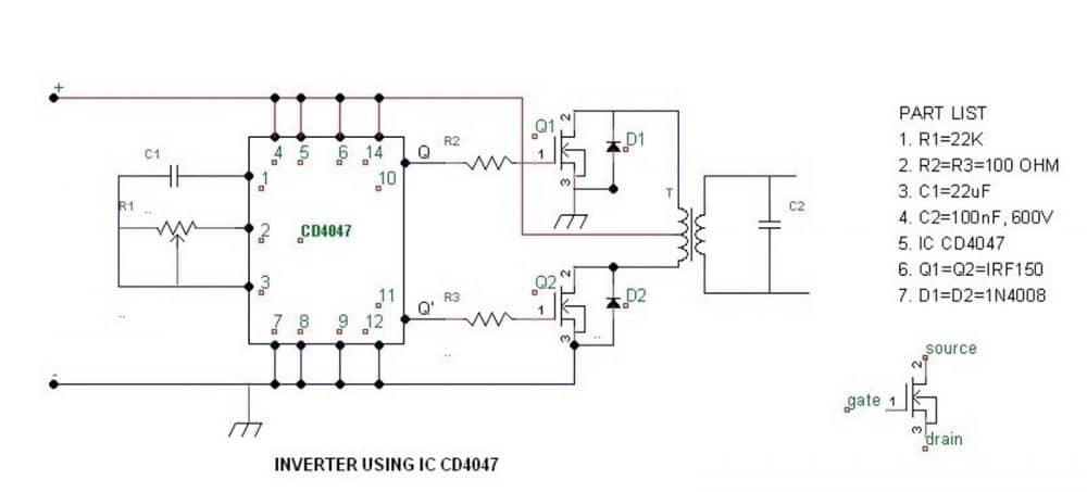
The IC 4047 section remains basically the same and is configured in its normal free running multivibrator mode with its output extended with the mosfet/transformer stage for the required 12V to the AC mains conversion.
How the IC 4047 Functions
The IC 4047 generates the usual square waves to the connected mosfets creating a mains output at the secondary of the transformer which is also in the form of square wave AC.
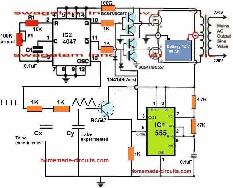
The integration of the two 555 IC to the above stage completely transforms the output into a pure sine wave AC. The following explanation reveals the secret behind the IC555 functioning for the above.
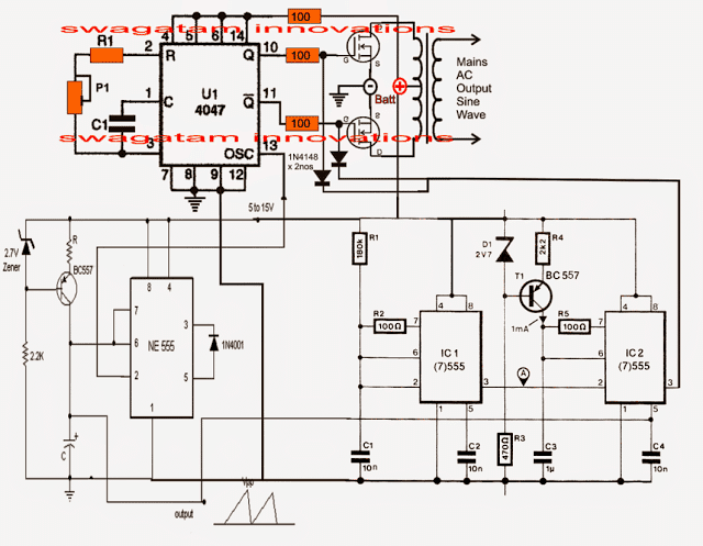
Referring to the below shown IC 4047 pure sine wave inverer circuit (designed by me), we can see two identical IC 555 stages, wherein the left section functions as a current controlled sawtooth generator while the right hand side section as a current controlled PWM generator.
The triggering of both the 555 ICs are derived from the oscillator output readily available across pin#13 of IC 4047. This frequency would be 100Hz if the inverter is intended for 50Hz operations, and 120Hz for 60Hz applications.
Using IC 555 for the PWM Generation
The left 555 section generates a constant sawtooth wave across its capacitor which is fed to the modulating input of the IC2 555 where this sawtooth signal is compared with the high frequency signal from pin3 of IC1 555 creating the required pure sine wave equivalent PWM at pin#3 of 555 IC2.
The above PWM is directly applied to the gates of the mosfets. so that the square pulses here generated through pin10/11 of IC4047 gets chopped and "carved" as per the applied PWMs.
The resulting output to the transformer also causes a pure sine wave to be stepped up at the mains AC secondary output of the transformer.
The formula for calculating R1, C1 is given in this article which also tells us about the pinout details of the IC 4047
For the NE555 stage C may be selected near 1uF and R as 1K.

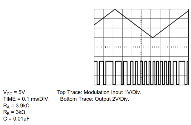
Assumed output waveform
More info on how to use IC 555 for generating PWM
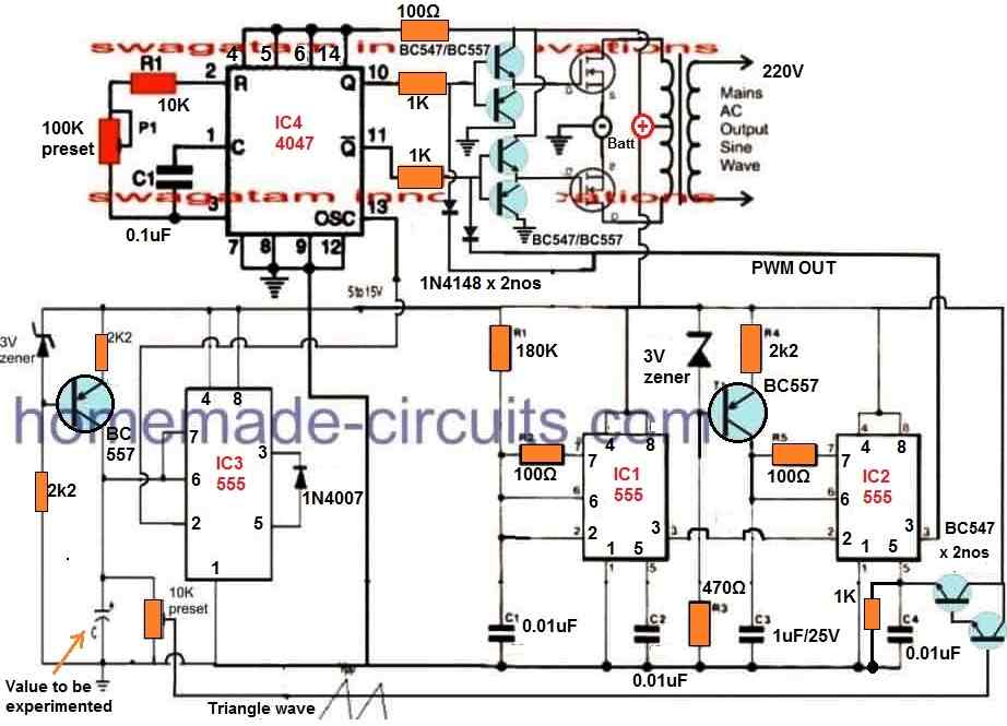
An RMS adjustment could be added to the above design by introducing a pot voltage divider network across pin5 and the triangle source input, as shown below, the design also includes buffer transistors for improving mosfet behavior
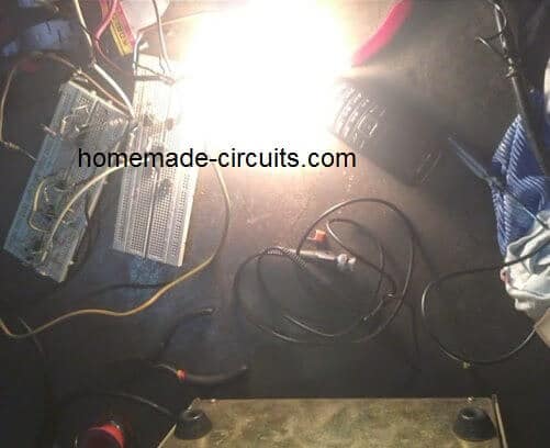
The above pure sine wave inverter design was successfully tested by Mr. Arun Dev, who is one of the avid readers of this blog and an intense electronic hobbyist. The following images sent by him prove his efforts for the same.
More Feedback
Inspiring response received from Mr. Arun regarding the above IC 4047 inverter results:
After completing this circuit, the result was amazing. I got full wattage by the 100 W bulb. Couldn't believe my eyes.
The only difference i had made in this design was replacing the 180 K in the second 555 with a 220 K pot to adjust the frequencies accurately.
This time the result was fruitful in all respects... On adjusting the pot, i could get a non disturbing non flickering full wattage glow in the bulb, also the 230/15 V transformer connected as the load gave a frequency in between 50 and 60 ( say 52 Hz ).
The pot was adjusted gently to get a high frequency ( say 2 Khz ) output from pin#3 of second ic 555. The CD4047 section better calibrated to get 52 Hz at the two output terminals....
Also I am facing a simple problem. I have used IRF3205 mosfets at the output stage. I forgot to connect the safety diodes across the drain terminals of each mosfets...
So when I had tried connecting an another load ( say table fan ) in parallel to the given load ( 100 W bulb ), the glow of the bulb also the speed of the fan was reduced a little and one of the MOSFET was blown due to the absence of the diode.
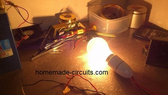
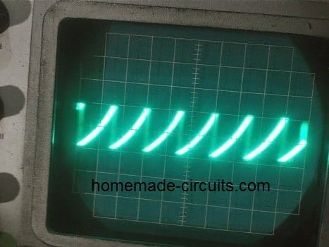
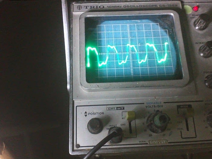
The above 4047 sine wave inverter circuit was also tried successfully by Mr. Daniel Adusie (biannz), who is a regular visitor of this blog, and a hardworking electronic enthusiast. Here are the images sent by him verifying the results:
Sawtooth Waveform Oscilloscope Output
Illuminating a 100 Watt Test Bulb
The following images show the modified waveforms at the output of the transformer as captured by Mr. Daniel Adusie after connecting a 0.22uF/400V capacitor and a suitable load.
The waveforms are somewhat trapezoidal and are far better than a square wave which clearly shows the impressive effects of the PWM processing created by the IC555 stages.
The waveforms could be probably even further smoothened by adding an inductor along with the capacitor.
Showing an near Sinewave Oscilloscope Trace after PWM Filtration
Interesting feedback received from Mr. Johnson Isaac who is one of the dedicated readers of this blog:
Good day
In your post, Pure Sine Wave Inverter using 4047, in the second I.c stage (ic.1) you used 100 ohms resistor in between pin 7 and 6.,
Is that correct? I use to think an astable multivibrator using 555 pin configuration should have the 100 ohms between pin 7 and 6. Also, the 180k variable between pin 8(+) and pin 7. Pls check the pin connection and correct me pls. Because it oscillate sometimes and it doesn't sometimes also. Thanks,
Isaac Johnson
Solving the Circuit Issue:
In my opinion, for a better response you can try connecting an additional 1k resistor across the 100 ohm outer end and pin6/2 of IC1
Johnson:
Thank you very much for your response. I actually constructed the inverter you gave in your blog and it worked.
Though I don't have an oscilloscope to observe the output waveform BUT I bet readers its a good one cos it operated a fluorescent tube lamp in which any modified or pwm inverter can't power on.
See the picture sir. But my challenge now is when I add load, the output flickers sometimes. But am happy its a sine wave.
Video Test Waveform
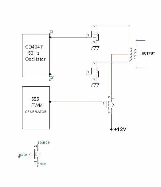
Simplifying the above Concept
The above explained IC 4047 pure sine wave inverter can be actually simplified greatly by eliminating two IC 555 configurations from the design.
The basic idea is to produce a synchronized sine PWM output for chopping the MOSFET switching so that this SPWM waveform is replicated at the output of the transformer and is transformed into a pure sine waveform. The complete circuit diagram can be seen in the following diagram:
In this simplified design, we yet again exploit the pin#13 square wave output from the IC 4047 and convert it into triangle waves. This triangle wave is then used to modulate the PWM output of a IC 555 astable to create the required synchronized SPWM for chopping the MOSFET gates.
The capacitors Cx and Cy will need to be experimented a bit to create a proper triangle waves from the RC network output.
Remember, you will need an oscilloscope to check and confirm the various waveform discussed in the above diagram.
Calculating the Cx and Cy Values for the Square wave to Sine wave Converter stage using RC Integrator
A 100 Hz frequency from pin#13 of the IC can only generate a crude sine wave using the shown double passive RC integrator circuit. We can make things easier by choosing the cutoff frequency fc to be pretty close to the fundamental frequency of the square wave which is fo and that happens to be 100 Hz. By doing this, we can reduce the higher harmonics a bit while still keeping that fundamental frequency intact. However if you want to get a decent sine wave, then remember we need to make sure that the input frequency is at least 300 Hz.
Formula:
The RC time constant relationship is:
fc = 1 / (2 * π * R * C)
R * C = 1 / (2 * π * fc)
For fc = 100 Hz:
R * C = 1 / (2 * π * 100) = 1592 * 10-6 seconds
Choosing Component Values:
First Stage (R1, Cx):
Choose R1 = 10 kOhms:
Cx = 1592 * 10-6 / (10 * 103) = 159.2 nF
Second Stage (R2, Cy):
Similarly, for the second stage:
R2 * Cy = 1592 * 10-6 seconds
Choose R2 = 10 k Ohms:
Cy = 1592 * 10-6 / (10 * 103) = 159.2 nF
Final Values for a Crude Sine Wave:
- R1 = 10 kOhms
- Cx = 159 nF (rounded to the nearest standard value)
- R2 = 10 kOhms
- Cy = 159 nF
Expected Output:
With these values our circuit will do a moderate job of cutting down those harmonics, and what we will end up with is a rough sine wave that has quite a bit of distortion. If you want to get things just right, you can tweak the values of the resistors or capacitors a little bit to fine-tune that waveform.
Another Simpler Looking Options
The following concept discuses a rather simpler method of modifying an ordinary square wave inverter using IC 4047 into a sine wave inverter through PWM technology. The idea was requested by Mr. Philip
Technical Specifications
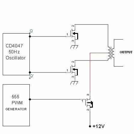
I hope that i am not going to be a bother, but I need some advice with a PWM-controlled modified sine wave inverter I am designing so I want to seek your expert opinion.
This simple design is tentative, I haven't implemented it yet but I would like you to take a look at it and tell me what you think.
Also I want you to help answer some questions which I have not been able to find answers to.
I have taken the liberty of attaching an image of a quasi-block diagram of my tentative design for your consideration.
Please help me out. In the diagram, the IC CD4047 in the inverter is responsible for generating square wave pulses at 50Hz which will be used to alternately switch on MOSFETS Q1 and Q2.
The PWM circuit will be based on IC NE555 and its output will be applied to the gate of Q3 so that Q3 will provide the PWM. Besides this, I have two questions.
First, can I use square waves for the PWM pulses? Second, what is the relationship between PWM frequency and supply frequency? What PWM frequency should I use for a 50Hz inverter output?
I hope that this design is feasible, I think it is feasible, but I want your expert opinion before I commit scarce resources to implement the design.
Looking forward to hearing from you sir!
Sincerely, Philip
Solving the Circuit Request
The configuration shown in the second figure above would work only if the center tap mosfet drain/source pins are swapped and N-channel mosfets are used for the 4047 inverter oscillator output, as shown below:
The PWM section should be built as I have explained in this article:
The PWM transforms the flat square waves into a modified square wave by chopping them into smaller calculated sections such that the overall RMS of the waveform becomes as close as possible to an actual sine counterpart, yet maintaining the peak level equal to the actual square wave input. The concept may be learned in details here:
However the above transformation does not help to eliminate the harmonics.
The PWM frequency will be always in the form of chopped square waves.
The PWM frequency is immaterial and may be of any high value, preferably in kHz.
How to Add Feedback Voltage Control to a 4047 IC Inverter
In this section we will discuss how to add an automatic feedback voltage control to a 4047 IC based inverter circuit.
If you don't want to read the whole explanation, you can watch the following video instead:
This type of feedback network is intended to ensure that the AC output voltage from the inverter never exceeds a predetermined safe value. For example, using this automatic feedback control, a 220 Volt inverter circuit output could be restricted to maximum 230V AC level, which may be safe for most 220 Volts appliances.
For a 120 Volt inverter system, this feedback network could be adjusted to restrict the output AC to a maximum of 115 Volts AC, which may be safe for most 110 Volt appliances.
How the Feedback Circuit Works
Now let's understand how the simple feedback network is designed to work, by referring to the following circuit diagram:
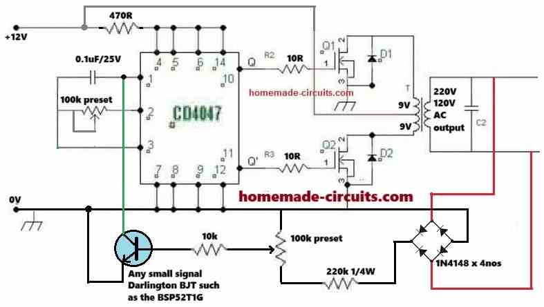
The mains AC voltage from the inverter transformer secondary is first converted to a DC voltage using a bridge rectifier.
This bridge rectifier is built using 4 numbers of 1N4148 diodes.
The DC 220 Volts output from the bridge rectifier is applied to an adjustable voltage divider network built using a 220 k resistor and a 100 k preset or trimpot.
The 100 k preset is carefully adjusted such that its central wiper terminal generates around 1.2 volts in response to an input AC voltage which is considered high, and needs to be restricted.
Let's say, the input AC needs to be restricted at around 270 Volts, then the 100 k preset may be adjusted so that its wiper terminal generates a proportional DC voltage level of 1.2 Volts.
We select a 1.2 Volt output because this is the equivalent DC level required to just switch ON the attached BJT device.
That means, whenever the inverter output AC voltage tries to exceed the 270 Volts mark, it causes the BJT to turn ON and become conductive.
When the BJT conducts, it starts grounding the CT pin of the IC 4047.
Since the RC network associated with the CT and the RT pinouts of the IC determines the output frequency and PWM, the grounding of the CT pin instantly causes the output PWM and frequency to nullify, which in turn causes the output AC voltage to dip.
When this happens, the feedback voltage to the BJT also drops proportionately until the BJT is turned off. In this situation the IC output PWM is restored back to its previous form, and if the output voltage continues to rise, it yet again activates the BJT via the feedback network, and this feedback on off cycle keeps repeating rapidly, ensuring that the output AC is not able to rise above the set threshold, which is 270 volts in our example.
This concludes our feedback control circuit explanation, now let's try to understand how this feedback circuit can be setup prior to integrating it with the inverter circuit.
How to Setup
The next diagram below shows the isolated feedback circuit, which can be set up by implementing the following steps, before interfacing it with your inverter circuit:
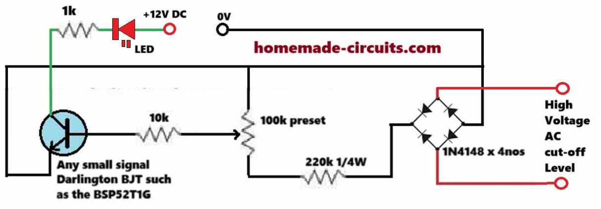
Initially keep the 100k preset's wiper arm fully towards the ground side of the DC supply.
Now, switch ON the 12 DC supply and then switch ON the AC supply to the bridge rectifier whose voltage level is around the desired high cut-off limit.
Next, slowly adjust the preset using a well insulated screw driver, until the LED just begins to illuminate.
To confirm the results, try varying the input AC voltage around the cut-off threshold and watch the LED turn on and off at the thresholds. Although the cut-off may not be too sharp, yet it will do the job of the intended output voltage control of the inverter quite well.
That's it! This simple procedure should be enough to complete the setting up of the feedback circuit.
After this, make sure to seal the preset adjustment with some super glue.
So, this concludes our explanation on a feedback circuit for the 4047 inverter.
Pseudo-sinusoidal IC 4047 Inverter Circuit
From a continuous source, battery, or vehicle alternator, it is possible to produce a 50 Hz voltage/pseudo-sinusoidal waveform, using this simple IC 4047 inverter circuit. The design is capable of operating many low-power devices that require a voltage of 220 V AC, typically supplied by the AC mains grid distribution network. The power of this module depends largely on the chosen transformer and, above all, on the continuous source's ability to supply the circuit without failure.
Working Principle of the circuit
Being able to power a device on the 220 V AC network when no mains AC power is available can be very convenient. We particularly think of campers, caravanners, fishermen, and motorists.
Although this simple setup does not provide a 100% clean sinusoidal wave, it can still satisfy many undemanding devices such as incandescent or fluorescent lighting, soldering irons, small motors, etc.
The power can reach up to 250 VA if the continuous source is strong enough and an adequate toroidal power transformer is chosen.
The power transistors are rated for 30 A, provided that a substantial heatsink is used.
We even suggest adding a small fan directly connected to the 220V output, which will prevent it from operating without a load.
Analysis of the Circuit Diagram
To obtain an alternating voltage from a DC source, the simplest solution is to use an inverted transformer: the low-voltage secondary winding has a center tap.
It is then sufficient to alternately supply power to the two windings to produce a symmetrical, but non-sinusoidal, variable voltage on the primary side if the low-voltage secondary winding is driven by a rectangular signal with steep edges.
Two complementary and opposite signals are required, and the CMOS integrated circuit with the reference 4047 is used to generate them, capable of either building an astable or monostable flip-flop.
The proposed diagram is shown in the figure below.
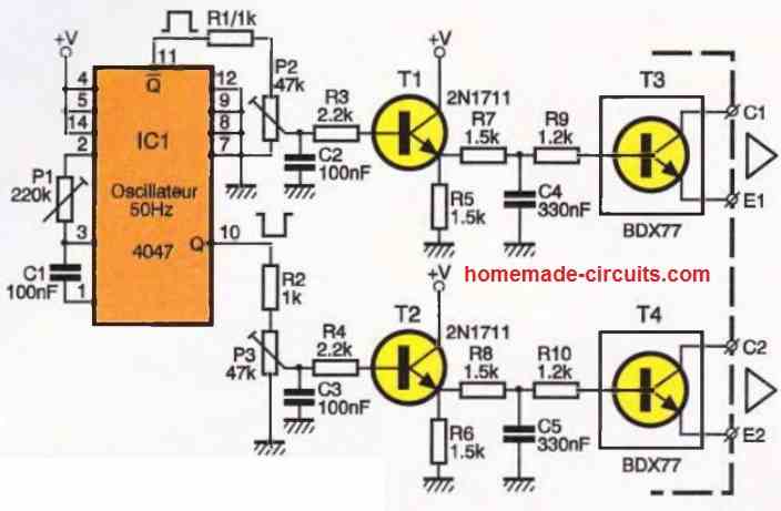
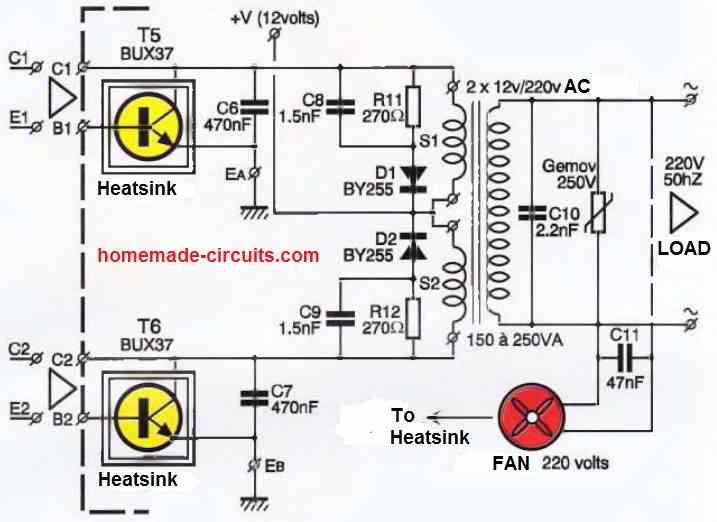
Of course, we will operate our circuit as an astable generator, ensuring a precise frequency of 50 Hz. This task is entrusted to components C1 and P1. Some pins of the IC1 circuit are connected to the ground or the positive supply, depending on our needs.
For more information, you will find an explanation in the appendix about the multiple possibilities of this practical little integrated circuit.
The symmetrical square voltages available at pins Q and Qdash (corresponding to terminals 10 and 11 of the circuit) are routed through resistors R1 and R2 to an adjustable element. Its role is to balance the amplitude of the two signals and facilitate the adjustment of the control module.
Note that the duty cycle will be exactly 50% by design. The sliders of elements P2 and P3 control the base of a 2N1711 transistor, which is responsible for driving the downstream power semiconductors.
Components R7, R9, C4, as well as R8, R16, and C5, form a coarse filter capable of smoothing out the signal angles to some extent.
This will allow us to create a "pseudo-sinusoidal" signal that will control the intermediate transistors T3 and T4 mounted on the small control board.
The BDX 77 models are rated for an emitter-collector voltage of 80V and a maximum peak current of 8A. They are delivered in a TO-220 package and will benefit from a heatsink.
The secondary windings of the transformer do have a common point connected to the positive pole of the power supply.
The other end of the coils will receive the ground through the power transistors T5 and T6, a model not much larger than the famous 2N3055 but with a maximum peak current of around 30A in this case.
It is the NPN bipolar model with the reference BUX 39.
Diodes D1 and D2 absorb the unavoidable breakdown current produced at each interruption of the inductive element, which is the transformer.
The primary of the transformer, a toroidal model in this case, delivers a 50 Hz AC voltage.
The component labeled Gemov (or varistor) is placed between the output pins to clamp excessive voltage surges that may occur.
Two wires can also be tapped from the output to operate a fan directly powered by 220V, which will provide airflow to cool the transistor-heatsink assembly.
It is important to ensure that the voltage of the continuous source does not drop too much or be completely depleted in the case of a lead-acid battery.
It goes without saying that the input DC current can reach considerable values if, for example, a power of 200VA is desired. It would be prudent to include a robust series fuse, similar to those found in a household installation.
Construction
The creation of two printed circuit boards is necessary: the first one, shown in the figure below, is designed for the components described in the control module.
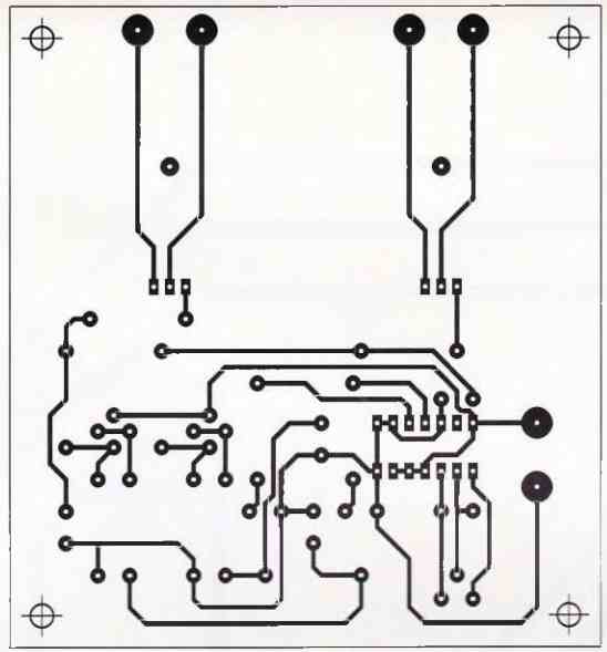
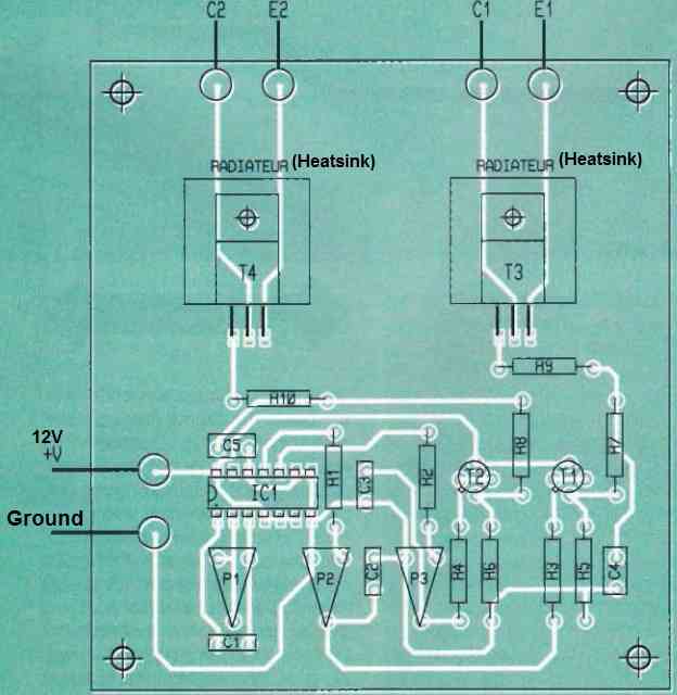
The layout is not very dense, but it is still recommended to use pre-sensitized copper-clad boards for reproduction.
After etching and rinsing, various drillings are carried out. Care must be taken to carefully mount transistors T3 and T4 on a small heatsink, which is directly attached to the epoxy board.
From this board, six wires will go to the significantly larger power module, and the track layout at a 1:1 scale can be found in the figure below.
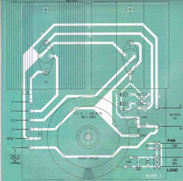
It should be noted that certain tracks on this simple IC 4047 inverter circuit board will carry high currents and require special treatment. We recommend soldering bare copper lengths, with a section of approximately 1.5 mm2, directly onto these tracks.
For example, electrician's copper wire with the insulation removed can be used. Care should also be taken to ensure all connections between the two boards, and in particular, to avoid reversing the wires.
The transformer has six wires, with the two thinnest wires corresponding to the primary, and therefore our 220V output.
It is important to properly identify the other windings before soldering them permanently. This assembly can be housed in a sturdy, adequately ventilated metal enclosure.
How to Setup
We leave it to you to complete this final step for this simple IC 4047 inverter circuit. After a thorough check, the frequency can be adjusted to 50 Hz under no-load conditions using the adjustable preset P1, if you have an oscilloscope or frequency meter.
Otherwise, simply set this element to the midpoint position. The other two adjustable components are set to obtain a symmetrical signal in amplitude.
Initial tests can be performed using a simple socket where different power lamps can be connected. For resistive or slightly inductive loads, there should be no serious issues.
Proceed with caution when testing devices that typically require a true sinusoidal voltage.
" rel="ugc">
Good day sir, thanks for your articles.
I have been trying to tweak various values of CX, cy ranging from pf to nf but the waveform was still sawtooth, please is there anything to do to improve the quality.
However, the inverter was able to power what ordinary modified square wave inverter could not power.
Thanks sir, I appreciate.
Good day Seun,
In the shown RC passive integrator circuit, the voltage across CX should be a sawtooth and the voltage across CY should be transformed to sine wave. It is a standard RC integrator circuit and should produce the intended results.
You must try try adjusting the resistors also.
Or you can try calculating the parameters using any online software, or online formulas and check the results.
Ok sir, thanks for the enlightenments. please what values and parameters to use, I couldn’t get any online calculator to use, please assist Me
Seun, I have updated the calculations in the above article for the Cx, Cy values, please check it out….
Thanks for your input. please what is the effect of crude sine wave and it’s meaning. is there anyway to enhance it?
It is not too crucial, even with crude sine at pin#5 of the IC 555, the inverter output will produce a decent sine wave provided it is appropriately filtered through capacitors at the output. You can use 3uF/400V PPC capacitors at the inverter output.
Thanks sir for your guide, I noticed the frequency generator produced 1.4Khz with R1 4,7k and R2 47k at the 555 timer does it have any implication?
Seun, 1.4kHz is high for an iron core transformer, it should not be more than 300 Hz, so please adjust the capacitor value accordingly.
The duty cycle will control the output voltage.
Thanks for the 4047 inverter design, it produced a good sine inverter, but I have issues build the trafo, please which transformer design for the input voltage for 12v design because of voltage drop.
Thanks Seun,
The transformer center tap voltage should be equal to the average voltage that you measure at the output of the PWM 555IC
I want to make a 24v inverter design, I used a voltage regulator for the circuit but I don’t know if to use 12-0-12 or 15-0-15 trafo, please kindly guide Me.
You can try 12-0-12V first, and check the results…
Thanks sir, can a range of trafo rating from12-0-12v to 18-0-18v work for 24v inverter system? please what is the effect in this variation.
Seun, a 12-0-12v to 18-0-18v trafo will produce a very high output voltage if the inverter is a standard square wave type, but if it is a sine wave PWM concept, then a 12-0-12V should work fine with a 24V battery.
sir, I am encountering a big challenge, As I complete this setup, I discovered that the 555 circuit is being damaged and the 12v regulator after working for 30minutes, please what could be the problem?
Hi Seun, please try connecting a 0.1uF and a 100uF capacitor, right across the pin#8 and pin#1 of the IC 555, and also connect a 12V zener diode across the same pinouts, and check the response…
Hello sir, the 555 timer is still getting burnt, please what could be the cause and what can I do?
Hello Seun,
Supply the pin4 and 8 of the 555 IC through this circuit, and check the response:
Also make sure to connect 1N4007 diodes between the center tap and the outer taps of the transformer.
" rel="ugc">
good day sir, I really appreciate your support here. you are doing a good job. please can this method of feedback be used with sg3525 inverter? I have tried using the FB pin but it’s not working.
Hi Hillary, please see the following diagram and see how the pin#1 of the IC SG3525 is configured:
" rel="ugc">
This takes care of the feedback control in the SG3525 circuit.
hello sir, how are you?
i want to ask on feedback point
can i use BC547 as a BJT device
or not?
Hello Sayed, yes BC547 can be used…
Hi Swagatam,
I sent you some more pics of what I was seeing at the 4047 and the 555 timer under different conditions. Please take a look at them and let me know what you can tell me about pics. I don’t know whatelse to try or what the problem could be with the 555 not producing PWM signals. I’ve replaced both chips multiple times and get the same results. I seem to come up with different cap and resister values for the 555 timer that are drastically different than what your schematic shows. Any ideas and/or pics that you can give me would be extremely helpful.
Thank you.
John
Hi John,
I checked the oscilloscope traces that you are getting, and when i joined the horizontal traces with corresponding vertical lines, I could clearly see the SPWM being generated at pin#3 of IC 555.
However, your triangle waves are not good, which may cause the SPWMs to be inconsistent.
Please investigate why the pin#2 triangle waves of your IC 555 are not good.
Initially try by removing everything from pin#5 of the IC.
The following are your scope images after I connected the horizontal traces with corresponding vertical lines.
Pin#13 square wave image: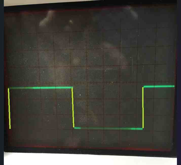
" rel="ugc">
IC 555 Pin#2 Triangle wave image:
" rel="ugc">
IC 555 pin#3 SPWM image: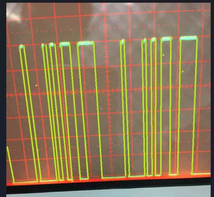
" rel="ugc">
Hi Swagatam,
I sent you more pictures for your evaluation and response. My scope does not show the vertial part of the traces for whatever reason, but let me know what you think.
Thank you
John
Hi John,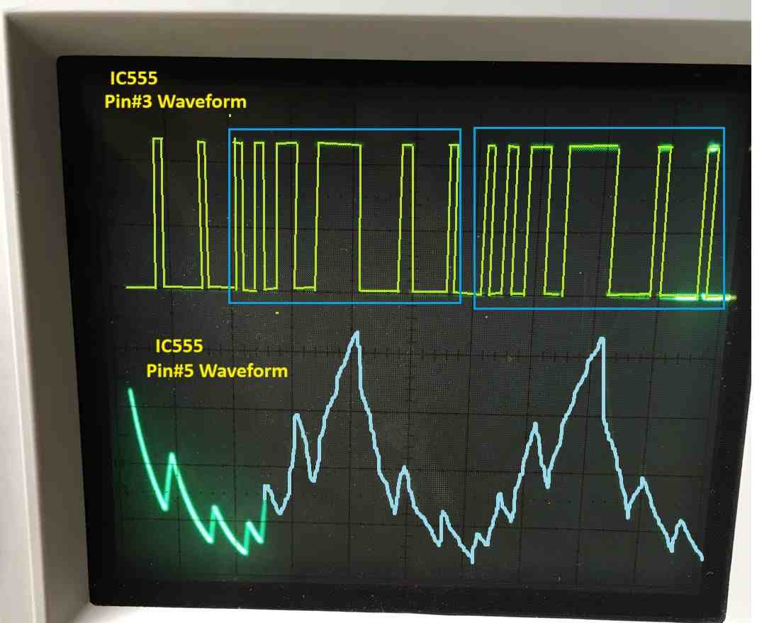
The SPWM looks somewhat good but not the ideal one.
Since the pin#5 triangle waveform is not smooth, rather very bumpy, it is causing the SPWMs to be unsymmetrical.
Could you please try adding a 0.1uF or 0.22uF or an appropriate capacitor across the pin#5 1k resistor and check whether the triangle waveform improves or not? You are very close to getting a perfect SPWM at pin#3 of the IC 555.
Here’s the waveform that you are currently getting.
" rel="ugc">
Hi Swagatam,
I tried the caps across the 1k resister at pin 5 of the 555 timer without any effect. I sent you some more scope pics and some more questions. Still don’t know what to do to correct this and appreciate your help.
Thank you
John
Hi John,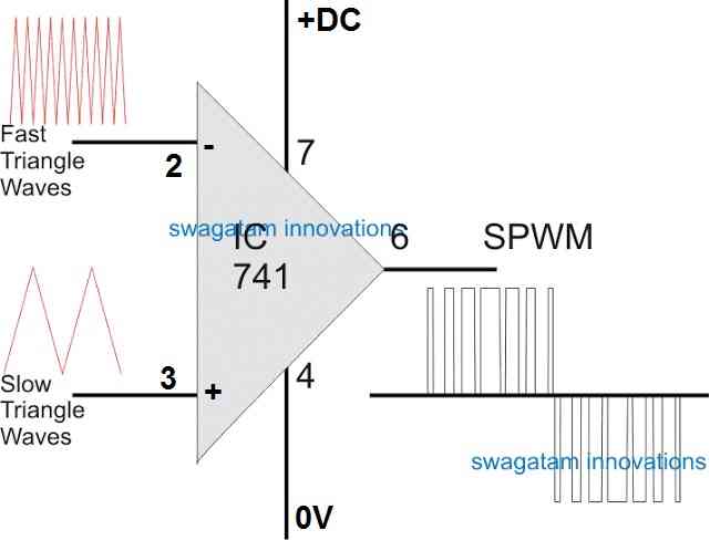
Even with the existing SPWM you might succeed to get a sine wave output, although not very symmetrical.
However, the question is why the triangle waves are getting spiked as soon as they are connected with the pin#5 of the IC 555. That’s strange and must not happen.
When I check the internal configuration of the IC 555, I find that the pin#5 is just connected to an opamp input and a potential divider.
Potential dividers and opamp input cannot themselves induce spikes on pin#5, so it is difficult to understand why you are getting those spikes on the triangle waves.
You can try adding a 100uF or a 1000uF capacitor directly across Vcc and ground pinouts of the IC 555 and check if the spikes disappear or not.
If not then you might have to simply replace the IC 555 SPWM converter with an opamp circuit, as shown below:
" rel="ugc">
Hi Swagatam,
I’ve struggled to get anything resembling a PWM out of the 555, until I drastically changed the resistor values. The resister value between pins 6 and 7 is 80K and the resister between pin 7 and 8 is 4.3K. I also changed the cap from pin 2 to Gnd to .015uF. Then it appears that I’m getting a PWM at pin 3 of the 555. I was going to send you some scope shots but was not sure if I could do that via comments. Let me know how to send scope shots.
In a previous message you told me to connect this up without a transformer and measure the rms value to determine the transformer ratio. I was trying to do this, but I’m using bench supplies of 12V in place of a battery. But this output stage is connected directly across the 12 volts and so draws more current than I can source. If I use a battery for the output stage it appears that it will just short out the battery drawing max current until something breaks? Now the rest of circuitry (555/4047) is connected to a different supply. Is it important that all of the circuitry is connected to a common 12v source (power supply) to control the overall current? Or can you explain how the current through the output FETs is controlled?
Thank you for all of your help
Thanks John,
I appreciate your efforts.
While measuring the average output voltage from the IC 4047, you do not need any transformer, and since no transformer is connected to the MOSFET drains, the drains are open, so the MOSFETs should not draw any current from the power supply or the battery.
The grounds of the two power supplies must be connected in common, otherwise the MOSFETs might fail to work.
Current through the MOSFETs will depend on the load current specifications across the secondary side.
To enable a current control you will need an external circuit which will initiate a grounding on the CT pin of the 4047 whenever an overload is detected.
Thank you Swagatam,
I appreciate all of your help!
I will continue to work on this an see what I can find out.
The other question that I had was if I could attach pics somewhere so that I could show what I was seeing. Is there a way of getting pics to you?
Thanks
John
No problem John,
You can send me the pics on my email ID:
homemadecircuits
@gmail.com
Hi Swagatam,
I was wondering if you got my pictures that I sent to you on the 7th via email? I seem to be stuck with this project until I get some input to tell me what stage of the circuit is not working properly.
Thank You for all of your help
John
Hi John,
I checked my emails and the spam boxes, I could not find any email from you.
Or you can upload the diagram to any free online image hosting site and provide the link to me here, I will check it out.
Ok I received your email, the PWM waveforms from the IC 555 are not clear.
Are you getting proper triangle waves across the 1K resistor at pin5 of the IC 555??
If you feed a triangle wave om pin5 of the IC 555 (across the 1k resistor) you should be able to get a proper SPWM at pin3 of the IC.
Hi Swagatam,
I forwarded the email that I sent before with the pics. Please let me know if you get it. I sent it to [email protected], I hope this is correct.
Thank You
John
Thank you John,
I saw the scope images that you sent. The triangle wave looks good but I could not understand any of the other images since the PWM waveforms are undistinguishable.
Are the triangle waves taken across the 1k at pin#5 of the IC 555? If yes, in that case you should be able to get a correspondingly varying SPWM at pin#3 of the IC. I am sure about this, provided the IC 555 is good.
Also can you please take the waveform image at pin#13 of IC 4047, that will prove your scope is producing the square wave pillars correctly or not. Does each pillar of the square wave appear separately and fully or are they produced as dashes only, we can confirm this at pin#13.
I guess you are working with this circuit:
" rel="ugc">
Hi Swagatam,
I have a few more questions;
1. What are transiters are used in the output stage to drive the transformer and where can I get the heatsink hardware?
2. What would be a good diode to put across the drain of the output FETs?
3. You told me a good transformer to start with would be a 9-0-9 5A. does that mean the primary has one winding with a center tap or …? Does the “9” represent turns ratio 9:1 in reference to the secondary. Also can you a step-down for a step-up interchangeably?
Thank you for responding when you have time.
Hi John,
1) The BJJTs can be BC547/BC557 pair, and the MOSFETs can be IRF540.
2) The diode can be a 1N5408.
3) 9-0-9 refers to 9V – 0V – 9v, which represents two winding with a center tap and would produce 9+9 = 18V if a 220V was applied from the 220V side of the transformer. Conversely, if this 9-0-9V side was switched by an inverter, it would generate a 220V from the 220V side of the transformer.
Yes, a step down transformer can be used to work like a step up transformer for an inverter.
Hi Swagatam,
Thank you for answering my questions, I’m sure many of them are fairly elementary to you.
I have just a few more and I hope to start acquiring the parts.
1. At this time I only want to generate 110V @60Hz. Is there a transformer that has a 9-0-9 on the primary and the secondary with a center tap to get both 220V and 110V? If so what would the nomenclature be?
2. For the simplified design you gave me, can you suggest starting values for the Cx/Cy caps?
Thank you again for your help.
Hi John,
The transformer that you are referring to can be termed as 9-0-9V / 5 amps / 110-0-110V.
However, please do not buy the transformer as yet, because the transformer primary winding voltage will depend on the average SPWM DC voltage value from the IC 555. You will have to first check this SPWM value and then buy the transformer accordingly.
You will strictly need an oscilloscope for testing and confirming the waveform. https://www.homemade-circuits.com/dso138-best-small-oscilloscope-for-electronic-hobbyists/
For Cy and Cx you can try 0.1uF initially and tweak them until you get a perfect triangle wave at 120 Hz, (60 Hz x 2 at pin#13 of 4047 IC)
Hi Swagatam,
I do have a scope (Tek 475) and plan on using a power supply for the 12V source. I have ordered some of the parts and am waiting for their arrival. How would you suggest I check the SPWM levels without the transformer. Can I leave the output transistor collectors open and measure the peak-to-peak voltage on each of the collectors, or do I need to have some kind of load in place of the transformer primary windings?
Hi John,
You can check the average DC voltage across the base of the bc547 transistors and the ground line, meaning connect the positive probe of the meter on the base of transistors, and connect the black probe on the ground line of the battery. No load is required because we only want to check the average dc produced by the spwm chopping. You can confirm the same across the gates/sources of the mosfets also. The drains of the mosfets can remain open while testing the above…
Hi Swagatam, I’ve been looking at this site for awhile and find that it has answered more of my questions than any other site I’ve looked at. I’ve been trying to determine where to get all of the components and hardware to start. The transformer is one of the main items that I’m having trouble finding. Do you have any suggestions where I might get this transformer? Also if anyone has some scope shots of the output of the different stages that would be helpful.
Thank you for all of your hard work that you have put into this website.
John
Thank you John, Glad you liked the site.
You can get all the parts from any online electronic spare part shop. There are many shops online that you can find.
You can even get the transformer from an appropriate online store. For experimentation you can start with a 9-0-9V 5 Amp transformer.
You will also need an oscilloscope to test and confirm the waveform across the various stages. I would recommend you to buy the following scope which is small, cheap and versatile:
https://www.homemade-circuits.com/dso138-best-small-oscilloscope-for-electronic-hobbyists/
For the circuit diagram, I think the following one is the easiest to build:
" rel="ugc">
Greetings Swagatam. Please receive my irrevocable appreciations and highest regards!
Thank you so much Ohonkpo.
Good day sir. Great work i must say. Please i have a question, where do i connect my oscilloscope probes to an inverter to measure the frequency?
Daniel, the best place is at the secondary or the 220V side of the transformer. However make sure to use a resistive divider so that the 220V is scaled down to a proportionate 5 V AC for the oscilloscope.
Good day Sir.
I’ve carried out tests on the inverter circuit.
I used 12v DC supply.
I didn’t connect the transformer.
I kept the IN4148 diodes disconnected from pin 3 of IC 2.
Here are the results I got:
Pin 10 & 11 of CD 4047 = 51.65Hz square wave
Pin 13 of CD 4047 = 104.2Hz square wave
Frequency across capacitor “C” = 104.2Hz square wave, and not triangle wave
Frequency across the wiper of 10k pot = 104.2Hz square wave, and not triangle wave
Pin 3 of IC2 is giving DC signal(horizontal straight line) with 157mV Vpp
Pin 3 of IC1 does not give any frequency, has 157mV Vpp
Pin 5 of IC 2 gives square wave with 3.76Vpp
IC1 is slightly warm
Please Sir, what could be the possible causes?
Hello Victor,
Your 4047 results are correct, but the IC 555 results are not correct.
The waveform across the timing capacitor C of a 555 will be always a triangle wave, because the capacitor is slowly charging and discharging which will cause a triangle wave across it. Are you using an oscilloscope to check the waveform?
IC1 pin3 must produce a square wave with a frequency above 100 Hz or 200 Hz, because it is a basic astable circuit.
So please correct the two issues. you must get a triangle wave across C.
and you must get a square wave frequency from pin3 of IC1
Yes sir. I used oscilloscope to carry out the test. I’ve tried testing again. Am still getting the same from 555 ICs.
Pls sir, what should I do?
I am thinking of testing the 555 IC with a test jig to know if it’s working well.
Pls sir, help me with a test jig for 555 IC
Victor, You will have to check and confirm the stages separately. If your IC1 stage is not generating a frequency then somethings wrong in that circuit, because all these circuits are well tested.
The IC3 stage is square wave to triangle wave converter circuit, which should convert the square wave from IC 4047 pin13 into triangle wave across the capacitor C.
Isolate all these stages and test the results separately.
If you still have problems, I will try to make the stages simpler for you.
Ok sir, thank you sir.
I would really appreciate making the stages simpler because I don’t know how to go about isolating the stages to test them separately.
Thank you very much Sir
OK, then first try building and confirming the following simple circuit. This concept shows how applying a varying voltage at pin#5 of a 555 astable produces a variable PWM at its pin#3. You can eliminate the mosfet and the bulb and R3.
" rel="ugc">
Good day Sir,
Please sir, help me with voltage divider circuit to convert the 220Vac from the transformer output to 5Vac so that the oscilloscope can handle.
Thank you
Victor,
you can take the help of the following page to calculate the values:
https://www.homemade-circuits.com/voltage-divider-calculator-software-potential-divider-calculator/
Thank you sir for the calculator.
Please Sir, I don’t really get the e24 and e96 series.
1. Which series is carbon and metal films resistors with 5% tolerance. Like the 220k, 10k 5% tolerance?
2. Also, am confused about the resistor scale(ohm).
Which scale is 220k, 10k , 100k etc ?
Thank you very much for your reply
Victor, you can read the following article regarding E24 resistor. You can select E24 in the calculator.
https://asenergi.com/pdf/resistors/standard-resistor-values-e24.pdf
For the scale range select the value which provides both the resistors in kilo ohms
i saw one of the UPS..the inverter section they have used Lm339 ic and ne555 and the transfomer is not center tapped,,its single…with mosfet z44..sir if you have such circuit or similar…help me..the ups bord was not clear
Hi Brian, I don’t have this circuit right now with me, If I find it I will surely let you know.
Is there any circuit available for 20w 24 volts dc to 24 volts ac inverter. can you help me about it?
I will try to design it for you….
Thanksgiving
Here’s the circuit you wanted:
" rel="ugc">
SIR, CAN WE PRODUCE 220 V 150 W (SINUSOIDAL) OUTPUT WITH THIS CIRCUIT.
PLEASE EXPLAIN…
Hi Amit, yes that’s possible, but you can build this circuit only if you are well versed with electronics and inverter concepts. If you want an easier circuit then you can try the following sine wave inverter circuit:
Arduino Pure Sine Wave Inverter Circuit with Full Program Code
Is there any circuit available for 150W 220V inverter other than arduino.
Or please suggest what should I change in this circuit to achieve it.
You can try the second or the third schematic from the following article:
https://www.homemade-circuits.com/modified-sine-wave-inverter-circuit-2/
Dear sir,
Once I have connected the battery, the circuit has burned. Can I connect 12V 45Ah car battery directly to the circuit without other components. Please help me sir.
Hi Hasai,
This circuit is a complicated circuit. It can be built successfully only if you understand each and every section of the circuit correctly and then implement it step-wise, using multimeters and oscilloscope. If you build it without understanding the stages and if you construct the whole circuit at once then surely the circuit may have a chance of burning due to a fault.
You will have to build and check each stage separately with an oscilloscope then slowly integrate each stage with one another. And before this you must first grasp and understand the working of all the stage perfectly.
Good day Sir.
It’s my pleasure to come across your website. I really appreciate your great work on electronics, and your offer of help on electronic circuit related problems.
As an electrical/electronics student/technician, I picked up interest of building this pure sine wave inverter circuit you designed (the second circuit from top with RMS adjustment), and I’ve viewed some comments.
Pls Sir, I would like you to help me with dis points:
1. I’ve built the entire circuit, where should I disconnect or section out to carry out stage by stage tests/checking on frequencies, waveforms and voltages before powering the entire circuit?
2. What points/pins should I check for the required frequencies & waveforms?
Pls sir include the required frequencies and waveforms at the points/pins
3. Will there be problem if the transformer is of higher capacity, while the battery and load are perfectly matched?
For instance, using 300VA transformer with 12V 7AH battery for a 12W load
4. I’ve used 7805 voltage regulator to supply CD4047 IC. I connected 100 ohms resistor to the IN pin of the regulator.
Then, I removed the 100 ohms resistor connected to the supply pins of CD4047 and connected the OUT and GND pins of the regulator to supply the CD4047 through a 10V/100uf capacitor.
Please sir, is it OKAY like that?
Pls Correct me if it’s not OK
5. In one of your replies to comments, you said for iron core transformer, each SPWM cycle should have 4 pillars. I don’t really understand d pillars.
Pls sir, what should be the actual PWM frequency that ensures there are 4 pillars in each cycle?
6. Generally, What is the maximum output wattage that can be achieved with 12V DC inverter system using a transformer?
6. Can the pure sine wave inverter circuit be powered to carry out test/checking on frequencies, waveforms and voltages without connecting the transformer?
7. Without connecting the transformer, can it be confirmed that the output AC waveform and frequency to be induced in the second side is sine wave and 50hz frequency by checking the waveform and frequency of the pulsating DC from the 3 wires to d primary side of the transformer?
8. For using headlamp bulb in series with battery positive, if the circuit connections are 100% Ok, will the bulb still light?
9. For capacitor C(value to be experimented), should the valued be selected 1uF and below or 1uF and above?
Thank you Victor,
Here are the answers:
1) Keep the diodes disconnected from the base/gate of the 4047 MOSFETs or the BJTs.
2) Check the frequency at pin13, it should be 100 Hz, and it should 50 Hz across pin10 and pin11. The waveform across the capacitor “C” must be a triangle wave. Pin3 of IC 555 will produce SPWMs or sine PWM with a frequency depending on the values of R1/C1 of IC1 555. This frequency will decide the number of pillars within each SPWM waveform.
3) Higher transformer power rating will have no problems.
4) You must use 7812 and not 7805 otherwise the MOSFETs might not conduct well. Capacitor across the 4047 supply terminals is OK.
5) If you see the image of a PWM waveform you will find they are made up of pillars or vertical blocks, or skyscrapers.
6) Maximum practicable power from a 12V inverter is 200 watts. Checking and testing the various waveform is possible without connecting a transformer.
7) They can be checked but ultimate confirmation can be achieved only after connecting a transformer.
8) If the circuit connections are OK, the bulb will not light up.
9) You can try with 1uF and check the triangle waves. Keep checking with different values until you get reasonably good triangle waves across “C”.
Thank you very much Sir for the answers.
Please sir,
1. Using 7812 voltage regulator now to supply the CD4047 IC, will the 100 ohms resistor on the supply pins of the CD4047 still be there or should be removed?
2. I also used one 7805 voltage regulator to supply the three 555 ICs.
please sir, Is it Ok or I should change to 7812 regulator as well?
3. How do I connect the oscilloscope probes to the three wires pulsating DC (fed to primary side of transfo) to check the waveform and frequency?
Thank you for your response, Sir.
Victor,
1) 100 Ohm should still be included even if a 7812 is used. Make sure to add a 100uF capacitor right across the 4047 supply pins and also a 12V zener diode paralel across the supply pins, this zener diode is for enabling the passage of reverse voltage spikes.
2) use 7812 or all the ICs, 7805 is not required anywhere.
3) Connect the ground probe to the drain of the MOSFET and the positive probe to the battery positive.
Okay Sir,
Thank you very much Sir.
Please, do I have to also connect 12v zener diode across 100uf capacitor supplying the three 555 ICs from 7812 regulator as you have mentioned in the case of CD4047 above?
2. Please sir, am also confused about this point: explain for me, please
Will the zener diode across cd4047 not function as voltage regulator also?
Cos from the 12v supply from the battery and the 100 ohms resistor in series with the battery positive, the voltage reaching the zener diode is less than its zener voltage(12v), meaning the zener diode will not conduct.
Thank you sir
The zener diode is not for 12V regulation, it is to make sure that if any reverse spike is present it can be shorted through the zener safeguarding the IC. You can replace the zener with a 1N4148 diode also.
Thank you very much Sir
Hello, I also made this project.
However, it does not work because the triangular wave that modulates pin 5 of the ‘SPWM’ generator is not centered on the square wave signal produced by IC4047. This can be seen thanks to the 2-channel oscilloscope.
How is it possible to center the 50 Hz. triangular wave of the first timer 555 and make the sawtooth crest fall in the middle of the square wave produced by IC4047 ?
It is synchronized with 4047 square wave signal. Please see pin#13 of IC 4047 which goes to the pin#2 of IC 555
Ing,,,, I can’t find the 3v Zener diodes,,, they only have 2.7V,,,4,7V…5.6V….8.2V….9.1V Ect
for sale, which could be replaced,, ,?
you can try 2.7 V zener, should work.
Dear sir,
Here, should we need to use 6V Fullwave (6Vx2) Transformer or 12V
Fullwave (12Vx2) Transformer. Please help me sir.
Hi Hasai, for a basic 4047 IC square wave inverter if the battery is 12V then the transformer should be 12-0-12V and if the battery is 6V the transformer should be 6-0-6V.
However since this is an SPWM based circuit, even with a 12V battery the transformer should be 6-0-6V or at least 9-0-9V.
The best way to confirm is to check the average DC at the gate of any one of the MOSFETs….that will be the value of the half primary winding of the transformer.
Ok sir. Is it enough 2 Ampere transformer?
If a 12V transformer is used then 2 amp rating will provide you with 12 x 2 = 24 watt output, which will be practically only 20 watts.
Thank you so much for your quick replies and great help sir.
I have a someone problem to clarify. Can you please explain, why we not need filter part here. How we satisfy filtering requirements in this circuit.
Hi Hasai,
For filtering the SPWM into a pure sinewave you just have to connect a 3uF/400V capacitor across the output wires of the transformer. The filter cannot be connected on the DC side of the circuit, that will not work.
Sir, is it ok we use 1mF capacitor for first test, will it blow out if it’s not Ok.
Hello Rncp, where do you want to use 1uF
Ok sir. Then can you please explain the reason for connecting the midpoint of the transistor to the positive of the battery? I can’t understand it. Why can’t we use a normal transformer?
It works in this way: The mosfets are configured to switch alternately using the oscillator frequency input. This in turn causes each half winding of the transformer to switch alternately using the battery 12V. When this happens the current from the transformer primary is induced into the secondary and stepped up to generate the 220V AC
Thank you so much sir
Dear sir,
Can you please explain,
1. what is the waveform of 3 rd pin of third 555.
2. should we connect midpoint of the primary winding of the transformer to the positive of batery. Then what type of transformer should we choice for it.(Center taped?)
1) The waveform at pin#3 of IC2 will be sine wave PWM.
2) Yes, the entire line which connects the center tap of the transformer must be connected with the positive of the battery.
Transformer should be a center tap transformer.
Dear sir,
Can you please explain How to connect midle point of primary winding in transformer to the positive of battery.
Hello Hasai,
You must connect it exactly as shown in the diagram.
Dear sir,
Where should we connect the negative side of the DC battery?
Carefully check all the lines which are shown with a ground or earth symbol. All those lines should be connected with the battery negative.
ok sir. Thank you so much
mr pleese 100w inweter circuit ferrit core trans former+
Hi, sorry, I don’t have a 100 watt ferrite core inverter design with me.
Dear sir,
1. what is the component P1 in circuit 1.
2. What is the component marked by the (+) which is in orange color near the transformer?
Please help me, sir.
Hasai,
P1 is a preset to adjust the output frequency of the inverter at 50 Hz or 60 Hz.
The orange colored + indicates the positive the battery. Battery positive should be connected at this point.
Dear sir,
What is the function of NE555 in the first circuit? Please explain
Hasai, all the 555 ICs are configured to generate sine wave PWM for chopping the 4047 50 Hz frequency
Dear Sir,
Please sir, I forgot to get clarified about the point:.
“The configuration shown in the second figure would work but only if the center tap PWM mosfet is replaced with a p-channel mosfet.”
I don’t understand it cos am using IRF3205, which is N channel, in the second circuit that has RMS adjustment.
Hi Godfrey, The “second circuit” is referred to the second last diagram, not the second circuit from top. I have updated the specific last section of the article, you can check it out.
Okay sir, I really appreciate your great and prompt replies. Thank you.
I am about carrying out some tests/checking for the Voltages, Frequencies and Waveforms on the circuit for 50Hz operation of the circuit.
I have supplied the ICs with 5V from LM7805 regulator
Please sir, I need your help on the following points:
1. What should be the required PWM frequency and voltage at pin 3 of IC2?
2. Which pot is used to adjust the PWM frequency?
3. The triangle wave of IC3 is at which pin? And what should be the required frequency and voltage at that pin?
4. What should be the required frequencies and voltages at pin 2 and 5 of IC2?
5. Which component/pot is used to adjust the Frequencies at pin 2 and 5 of IC2?
6. What should be the required voltage at pin 3 of IC2?
7. Is it OK to still add the 100 ohms resistor after LM7805 to the supply pins of cd4047?
8. What should be the required voltage at the gate of the mosfet?
9. What should be the required voltage at pin 10, 11 and 13 of CD4047?
10. Apart from the drain pins and batt +Ve to the 6-0-6V side of the transformer, which is AC. Are the above tests/checking to be set DC? That’s connecting black meter probe to the ground of the circuit and red probe to the points to be checked?
11. In situation where small portable oscilloscope can’t handle 220vac of the transformer output, can 50Hz frequency and Sine wave check on the 6-0-6V input to the transformer be judged as what the transformer is outputting on the 220V side?
12. Is it necessary to connect a capacitor, for smoothing purpose, across a 12V input supply to the inverter circuit, even when using 12V battery? If so, what value can be used?
13. The capacitor C ( i.e value to be
experimented), is the value to be chosen below 1uf or above 1uf?
I would be glad for your help.
Thank you
Godfrey, here are the answers:
1) If you are using an iron core transformer, the SPWM frequency at the pin#3 of IC2 should be 200 Hz, or in other words the PWMs should have 4 blocks or 4 pillars on each cycle.
2) The value of the capacitor C of IC3 and the associated 10K preset decides how the PWM pillars vary its thickness. It does not decide the frequency, I was wrong in the previous comments.
3) The adjusted triangle wave can be measured across the preset output, and the non-adjusted triangle wave can be measured across the capacitor C. The frequency will be same as the frequency generated at pin#13 of 4047.
4) The frequency at pin#2 of IC2 needs to be adjusted by adjusting the value of the R1 180K resistor or C1. This resistor actually also decides the SPWM frequency. You will have to play with the 180k value to finally adjust the SPWM frequency so that it has around 4 to 5 pillars in them. pin#5 receives the triangle waves whose amplitude can be adjusted with the IC3 10k preset.
5) The 180 K and the C1 values decides the frequency at pin#2 of IC2.
6) The voltage at pin#3 of IC2 is a SPWM varying voltage which will have an average value depending upon how the 180K and the 10k preset are set.
7) Use a 7812 Ic and a 22 ohm resistor, along with a capacitor, and a zener diode protections across the supply pin of the 4047.
8) The peak voltage at the mosfets gate will be 12V, and the average voltage will be 6V without the SPWM added.
9) All these will ahve peak voltage equal to the supply voltage of the IC, average voltage will be according to the frequency outputs of the pins
More answers will be provided in the next comment.
10) All the points on the transformer primary side are either DC or pulsating DC, they are not AC. AC is only at the secondary side of the transformer. You will ahve to measure all the battery side connections with respect to the black probe connected to the ground line.
11) To measure the output side 220V create a voltage divider using a 220K/10k resistor or something like that which will convert the 220V AC sine frequency into 5V AC sine frequency and then you can comfortably measure the secondary side sine wave.
Remember mains AC from inverter is dangerous and lethal, you are doing all these testing at your own risk.
12) It is always good to add a high value capacitor across the battery terminals to absorb voltage spikes.
13) You can start with 1uF and check how it responds, and then you can use other values to verify that the SPWM pillars are distributed uniformly across each cycle of the AC.
Thank you very much sir for your time and effort in providing the answers.
Please sir, am very very confused about point 10, that “all the points on the transformer primary side are either DC or pulsating DC.”
Because I learnt that transformer works on AC only. That is, applying an alternating voltage to one side usually the primary, then an induced voltage by electromagnetic induction appears at the secondary side.
Please sir, I want to get clarified if iron core inverter transformers don’t have the same working principle as ordinary iron core transformers?
Thank you sir
Godfrey, transformer works using pulsed DC and AC both. Pulsed DC means any DC which switches ON/OFF alternately. AC is a supply which changes its polarity from + to – and then – to + alternately, this is not mandatory for a transformer to work. The mosfets are switching DC across each half winding of the transformer, they are not switching AC. But the center tap winding are configured with each mosfet in such a way that when both the winding are switched alternately, it causes an AC to generate across the secondary. Each of the mosfet is creating pulsed DC on the primary side of the transformer which is causing an AC to develop on the secondary side of the transformer.
Okay sir. I have got the principle now.
Thank you
No problem Godfrey!
I think you can get a ready made triangle wave across timing capacitor of 4047 IC, and you can use this triangle wave to feed the pin#5 of the IC2, in this way you can eliminate the IC3 completely.
Dear Sir,
Thank you for updating the second circuit.
Please sir, the capacitor c across 10k preset (i.e “Value to be experimented”)
1. I have already used 1uf/50V, please sir is it within the values to be used?
2. Please sir, how does the value used affect the performance of the circuit?
As in, why the value need to be experimented.
Thank you sir
Thank you Godfrey,
The capacitor C determines how many pillars each SPWM cycle will have from pin#3 of IC2. If you are using an iron core transformer then you must make sure the number of pillars in each SPWM cycle does not exceed 4nos otherwise the transformer might heat up. You must have an oscilloscope to check how many pillars in each SPWM cycle you are getting for the selected capacitor.
Okay sir. Thank you so much.
Please sir, I’ve googled to know what is pillar in SPWM, I can’t find answer..
Please sir, what’s pillar?
Thank you
Hi Godfrey, By “pillars” I meant to indicate the number of blocks in a PWM cycle. You can see it in the following example image:
" rel="ugc">
Okay sir, thank you.
Please sir, to get you very well.
Using the image u sent, how many cycles are there in that PWM?
2. Then, Each of the pwm cycle contains how many pillars?
Thank you sir
The number of blocks is not a fixed number, higher the number of blocks, cleaner will be the sinewave and vice versa. But higher number of blocks would also cause the frequency of the PWM to increase, adversely affecting the working of an iron core transformer. Therefore you have to limit and optimize the number of blocks in such a way that you get a reasonably good sinewave and the transformer also remains cooler.
For the diagrams shown in the above article, the number of pwm cycles will be equivalent to the frequency at pin13 of the 4047 IC, and number of pillars or blocks will depend on the triangle wave amplitude, generated by the IC3
Thank you so much sir
My pleasure!
Dear Sir,
Please sir, I have finished building the second circuit that has RMS adjustment.
Please sir, I want to know the terminals I have check with Frequency meter and Oscilloscope to get the expected frequencies and waveforms for 50Hz operation of the inverter.
Thank you sir!
Hi Godfrey,
Initially do not connect the IC2 555 pin3 output with the transistors of the inverter. First check the inverter without this connection. Confirm the 50 Hz frequency at the inverter output with 220V. Check this with a load bulb
Once confirmed, next check the triangle waves at pin#5 of IC2 555, and also check whether pin#3 is generating the required sine wave PWM or not….
Once confirmed only then integrate the pin3 output of IC2 555 with the inverter transistors.
Okay sir, thank you so much.
Please sir confirm this additional things I have done if they are OK before I power the circuit:
1. I have connected IN5404 diode across the S/D of each mosfet.
2. I have connected 1k resistor across Gate/Source of each mosfet.
3. I have connected 100ohms resistor across the emitters of bc547/557 and the gate of each mosfet(gate resistor).
4. I have used 7805 ic to power only cd4047 ic and another 7805 to power only the three 555 ICs while the rest circuit remains the way u designed.
5. I used a 100uf/25v cap for the IN pins of the 7805 ICs and 100uf/10v cap each for the OUT pins of the 7805 ic
Please sir, are all the above OK?
Or any change needed for the capacitor values and so on?
Then, I saw in one of your replies to comments advising the person to connect a 12v car headlight in series with the battery positive to tackle some heating issues. Please sir, is there need for me to also do so?
Thank you very much sir.
Godfrey, yes all those points are prefect and can be applied to the second schematic! A series headlamp initially ensures that if something is not correct in the circuit then nothing will burn, instead the bulb will illuminate and prevent anything from burning. If you are 100% sure that nothing is wrong in your circuit then the bulb is not required.
There’s one thing that seems to be missing in the schematics, it is a 1K resistor across C4. Please add a 1K resistor across C4
Dear Sir
Please sir, I have connected a diode to S/D of the mosfet for Avalanche protection.
Please sir, can I add Gate/Source Resistor for another protection?
Yes you can add a 1K resistor across gate/source of each mosfet for more efficiency.
Dear Sir,
Please sir, if I wish to power the ICs with 5v, can I use one 7805 voltage regulator to power the three 555 ICs?
Hi Godfrey, yes that’s fine, you can do it.
Thank you very much sir
You are welcome Godfrey.
Dear Sir,
I have seen HA17555 ic in market,
pls sir, is it the same as CMOS 7555 ic?
2. I wish to replace the 180k resistor with 220k preset in case of necessity for frequency setting, but 500k preset is handy for now.
Please sir, can I used the 500k preset?
Dear Godfrey,
It seems both the ICs are the same. HA17555 is a CMOS version of IC 555
You can use 500k resistor instead of 180K
Thank you sir
Dear Sir,
Please am trying to build the second design that has RMS adjustment and buffer transistors.
1. Is the circuit diagram/components Okay or new any modification/update is done?
2. What should be the frequency at pin 10, 11 and 13 of CD4047 IC for 50Hz operation of the inverter?
3. What are the fixed values of C1 and R1+P1 for CD4047 for 50Hz operation of the inverter?
Thank you very much sir for response
Dear Godfrey,
yes the circuit components are OK. Just make sure to add a 12V zener diode across the supply pins of the 4047 IC, and also add a 100uF/25V capacitor across the supply pins.
The frequency at pin 10, 11 should be 50 Hz, at pin13 it should be 100 Hz, but all these should be confirmed with respect to the output AC frequency.
The C1, R1+P1 will need to be set by checking the frequency at the output of the transformer. initially you can take C1 as 0.1uF, R1 as 22K, and P1 as 100k preset.
Okay sir,
Please sir, is the zener diode to be connected in reverse bias as voltage regulator? That is, the anode to the GND of the Cd4047 and cathode to the Vdd of the cd4047?
Yes that’s correct.
Hi Mr Swag, nice job here
I just stumbled across this website and wanted to let you knowhow much I anticipate studying it. It will most likely take a while but I am sure you will hear from me down the road. If you’re an amateur radio enthusiast, you probably saw the call in my email address but I no longer hold that call. I exchanged it for W4PFC. I have been tinkering with electronics since the early 50’s and can hardly wait to get familiar with your web site. I have some hefty projects in mind.
Sincerely,
Rich Ferguson
Flagstaff, AZ
Thank you for your kind feedback, appreciate your interest!
Mr Seagate, my problem here is how to connect inverter with battery charger and auto switch. Please help out with simple circuit diagrams showing these connections. Thanks for the usual responds.
Stephen, please refer to the following article, and customize your design accordingly:
https://www.homemade-circuits.com/how-to-make-mini-homemade/
Dear sir,
Please sir, I can’t find the 1uF non polarized capacitor (C3 at the bottom right of the circuit) in the market.
Please sir, what other value can I use or can I replace it with 1uF 50V electrolytic capacitor?
Godfrey, you can use polarized cap also, since the negative terminal is directly connected to the ground line…
Okay sir, thank you!
Dear sir,
Please sir, for the polarized capacitor C which is connected across the 10k preset in the second circuit,
Can I use 1uF 50V electrolytic cap. Or
a lower value (say 0.33uf or 0.47uf)?
Thank you
Yes you can use 1uF or lower values will also do….
Dear sir,
Please sir, for a 600VA transformer, if the max output power of a transformer is 360W.
In a situation where a 12V, 30Ah battery for delivering 360W for one hour is not handy
Please sir,
1. Can I use a 12V, 25Ah battery to deliver 100W to run a load of 100W for 3 hours?
2. Can I use the IRF3205 mosfet in the pure sine wave inverter with RMS adjustment for the 12V, 25Ah battery to run the 100W load for 3 hours?
3. To calculate the inverter supply current in order to know the protection diode to use across S/D pins of the mosfet, please sir, will it be 100watt / 220V inverter supply voltage = 0.45A if am using the 12V, 25Ah battery?
Hello Godfrey,
1) you can 25 Ah battery for running a 60 watt load, not a 100 watt. You must discharge the battery at a maximum 15% of the Ah value
2) You can use IRF3205
3) protection diodes can be rated at 5 amps which is the recommended discharge rate of the battery, or the operating current for the inverter with a 25 Ah battery
Okay sir, thank you for your reply!
Please sir, to get you very well about the 15% max discharge.
1. Do you mean that, though the 12V, 25Ah can deliver a Max power of 100W for 3 hours, it must not be used to run a 100W load even for a very short time, say 5 minutes?
2. Please sir, in a general view, what is the recommended discharge rate or the max percentage discharge for a battery with respect to its Ah value?
3. Please sir, how do you calculate the 5 Amps discharge rate of the battery and the operating current of the inverter?
Godfrey, there are no fixed parameters in electronics, all parameters are relative and approximate values.
A lead acid battery must be charged or discharged at around 10 to 15% of its Ah rating to prevent cell deterioration. Therefore for a 25 Ah, the maximum discharge current should be around 4 amps, and not 5 amps.
So if yo multiply 4 amps with 12 V, gives 48 watts, so that’s the maximum load recommended for your inverter.
Now Ah = 25, and considering A = 4 amps
we have
h = 25 / A
h = 25 / 4 = 6 approximately, which is 6 hours back up time in ideal situation, practically it may be just 3 to 4 hours due to many hidden losses.
Okay sir, thank you very much
Dear sir,
Please sir,
1. From the theoretical 6 hours, what is the formula to calculate the actual time the battery should be discharged practically?
2. Please sir, If the current rating of my system is between 1.12A to 1.44A, can I use 1A diode like IN4007 for the avalanche protection?
3. Please sir, will increase in the resistance of the 10K preset from 5K upward increase the RMS output voltage of the inverter to the rated value or decrease it?
Hello Godfrey,
1) Please read the article Lead Acid Battery Charging
2) Yes, that will do
3) Moving the slider towards the capacitor positive will increase the RMS and moving it toward the ground will decrease the RMS
Dear sir, please sir can I use IRF3205 MOSFETS for the pure sine wave inverter circuit with RMS adjustment?
yes you can use it….
Thank you sir
Dear sir,
Please I have a 10A ups transformer having four wires(black, blue, green and yellow) on the primary side and two fat wires on the secondary side.
When I applied 220V across the black and blue wires, I got 14V from the secondary.
Please sir I want to know if I can disassemble and centre tap the secondary to be 7-0-7v , and then use it for the above pure sine wave inverter circuit you designed?
Hello Godfrey, you can do that, just pull out a center tap from the middle of the 14V winding….and then you can use it for making any center tap transformer based inverter
Dear sir, thank you for all your tutorials on pure sine wave inverter circuit. I really appreciate it.
I wished to have been done building, testing and confirming your great design and work on this inverter circuit diagram by this weekend, but just one part of the components is keeping me. I have searched through many electronic part shops in my area. I can’t find the a TRANSFORMER with the 10A current rating you recommended for me. The highest current rating seen in all the shops is 2A.
I saw 240/15-0-15v, 2A transformer (iron laminated):
1. Please sir can this transformer be disassembled and rewound based on specifications to output 9-0-9v, 10A you recommended for me to use for 60W inverter circuit?
2. I have also seen a UPS transformer during my search for 9-0-9v, 10A transformer.
The UPS transformer has four wires on the low voltage winding and two wires on the high voltage winding.
Please sir can the UPS transformer be useful for the inverter circuit in question?
3. I would really love to design and build my own inverter transformer, please sir I would appreciate my help on how to design and build the transformer and the materials I need to use.
Although I have read your post on “how to design your own inverter transformer”, I am not getting it well. Please sir throw my light.
Thank you for your time.
Hi Godfrey, yes you can rewind the transformer for higher current if the space between the core allow the accommodation for the winding.
2) transformers are all similar with their working principles, so UPS transformer will also work.
3) Transformer designing should be done only with the recommended formulas, so you will have to follow the mentioned formulas in the article, there’s no other easy method.
Alternatively, you can also refer to the following article for more info:
How Transformers Work
Thank you very much sir!
Please sir concerning the UPS transformer, the one I have has four small wires on one winding (i.e black, blue, green and yellow wires),
and two fat wires on the other winding(i.e blue and red wires).
I didn’t know which winding is primary and which is secondary.
So I downloaded two videos on YouTube about the transformer.
From the two videos, i learnt that the winding with four wires is taken to be the primary, and was supplied with 230v mains. The black wire from the four wires was the COMMON. So from the voltmeter that was connected across the two fat wires(as the secondary), when 230v was applied across black and blue, the voltmeter read 14v; black and green = 5v; black
and yellow = 7v.
1. Please sir my question is how can I use this transformer with the above pure sine wave inverter circuit you designed? How will I connect the transformer to the circuit?
Thank you sir.
Godfrey, the transformer ratings cannot by assumed by guessing, you must check it practically by feeding the 220V on the primary side and then checking the corresponding voltages on the secondary. If the voltage matches the specifications provided in the above sinewave inverter circuit only then you can use it, otherwise not.
Alright sir. Thanks very much sir for your time!
So there’s no 22k resistor in the circuit, please sir any need for protection diode for the MOSFET?
You are welcome Godfrey, yes there’s no 22k in the diagram, you can add external protection diodes across S/D pins of the MOSFETs for increased safety
Okay sir, thank you very much.
Let me go about with the design.
Dear sir,
1. Please sir can I mount the two IRF540 MOSFETs on one heat sink? Or if the two mosfets are not to be mounted on one heat sink, can I use heat sink insulator pad or use two heat sinks separately at once?
2. Please sir what protection diode can I connect across the S/D pins of the mosfets? And also which terminal of the diode (cathode/anode) is connected to the D pin and the S pin of the mosfets?
Thank you sir!
Hello Godfrey,
1) yes you can mount two MOSFETs on a common heatsink, preferably you can use heatsink insulator with them.
2) You can use a diode with current rating equal to the current rating of the inverter, cathode will go towards the positive supply line, and anode towards the negative supply line.
Okay sir, thank you sir!
But am confused somewhere: I don’t know how to get the current rating of an inverter. Please sir help me with the formula for calculating the current rating of an inverter.
Thank you
Please divide wattage of the inverter with its voltage
Dear sir, I would like to sieze this opportunity to thank you for your time and the great offer of help you have made tutoring electronic engineering lovers in circuit designs. I really appreciate it.
Please sir I would like to build the pure sine wave inverter circuit using IC 4047.
I want to go for your second circuit diagram which has RMS adjustment and buffer transistors for improving mosfet behavior.
Please sir I have some questions I want to get clarified about the circuit.
Q1. In your post on IC 4047 data, you said R1, P1 and C1 determine the oscillator frequency of the IC and the output at pin 10 11 and 13. Please sir, what value of R1 and C1 should be used and what resistance value should P1 be set to in order to get 50Hz source frequency from the inverter?
Because I haven’t seen the formula for calculating R1 and C1 in this article and also frequency meter is not handy with me for now.
Q2. Please sir what is wattage of the resistors used in the inverter circuit?
Q3. Please sir, the 10K preset, is it for RMS adjustment? Is the RMS adjustment responsible for output voltage of the transformer inverter? And also what resistance value should it be set to?
Q4. Please sir, the 10nF and 1uF capacitors, can I use ceramic or polyester type? Again, what is the voltage of the capacitors? Also what is the voltage of the capacitor C = 1uF at NE555 stage?
Q5. Please sir, do I need to work with these formulas in order to ensure good performance of the inverter?
f = 1/8.8RC at pin#10 and pin#11
f = 1/4.4RC at pin#13. of IC 4047
Pulse time, t = 2.48RC
Q6. Please sir, is the NE555 the same as IC (7)555 ?
Q7. Please sir, is there wattage of the 3v zener diode considered or any 3v zener diode is Ok?
Q8. Please sir, is the circuit diagram Ok or any modification needed?
Finally, what core type is used for the inverter transformer? Again, what is the minimum specifications for the center tap transformer and the battery to be used in order to get 100W output from the inverter.
Thanks very much sir for your anticipated effort and time to through all these questions. Looking forward to hearing from you.
Hello Godfrey, here are the answers for your questions:
1) You can use 56k for R1 and 0.1uF for the C for approximately 50 Hz output.
2) All resistors are 1/4 watt 5% and capacitors can be disc ceramic or PPC for the non polar, and electrolytic for polarized. 1uF can be a polarized capacitor.
3) yes RMS can be used for fixing a constant 220V/120V output
4) All capacitor voltages should be at least 2 times the supply voltage.
5) You can confirm the frequency with a frequency meter, calculating using formulas is not necessary.
6) NE555 is analogue, and 7555 is CMOS, both will work
7) 3V zener can be a 400 mW zener
8) Circuit is OK.
transformer core is iron laminate. specifications will be 6-0-6 /18 amps/ 220V for a 12V battery 100 watt
battery should be rated at minimum 25 Ah
Thank you very much sir for your great tutorial.
Please sir am not getting this point well
“All capacitor voltages should be at least 2 times the supply voltage.”
1. Please sir, is it with respect to the supply voltage of the entire inverter circuit (which I will use 12V lead acid battery) or is it with respect to the voltage across the individual capacitors?
2. Please sir can I use disc ceramic capacitors rated either 25v, 50v, 100v or what voltage, out of the three voltage ratings will be Ok? because I want to use 12v lead acid battery for the inverter circuit.
3. Please sir, another thing is, I may no longer want to go for 100W output power from the inverter since the transformer and battery specifications for the 100W power output seem unreachable for me for now.
However, my intention is to power 5pcs of 10W/220V/50Hz LED bulb lights for about 4 hours daily after full charge of the battery before in use. I also want to leave an extra power of about 10w in the inverter. So please sir, what specifications of transformer and battery will be fit to power the five 10W/220V/50Hz LED bulb lights and still retain 10w power in the inverter?
Thank you sir for your time!
Hello Godfrey,
the rule of thumb is to use capacitors having voltage rating two times the supply voltage from the power supply, in your case it should be 24V or higher.
This is true for all the capacitors.
The transformer for the mentioned inverter specifications can be a 9-0-9V 10 amps/220V and the battery can be rated at 12V 20 Ah
Thank you very much sir for the tutorial. I really appreciate your time and effort.
Glad to help!!
Dear sir, please I forget these points:
1. What is the MOSFET value for the second circuit with RMS adjustment?
2. What Is the value of the electrolytic capacitor C at NE555 stage of the circuit?
3. Please sir the value of the resistor between zener diode and the electrolytic capacitor on the left side of the circuit is not seen clearly. Please sir, is it 22K or 2.2K?
Thank you very sir!
Dear Godfrey, 1) The MOSFET power handling capacity will dependent on the power spec of the inverter. For moderate power you can use IRF540
2) you can use 10nF ceramic disc for the C.
3) It is 2.2k
Hello everyone! I need help! I made a simple inverter and when there is no load the voltage is 220V but when I plug in the load it becomes 30V. The load is 80W
Hello Swagatam ! What is the value of P1 between R1 and pin 3 of 4047 IC ? please tell me this only one you leave.
Hello Than, it is a 22k preset
Thank you so much! Swagatam
My pleasure!
Thank you so much sir swagatam, you have solved my problems.
You are welcome Evans!
sir can you look at this circuit
" rel="ugc">
will it work or any kind of modification needed.
Shankar,
yes it will work….no modification needed
thank you sir for your valuable comments.
sir why are you inactive in youtube now?? any reasons
sir i dont understand the circuit in given website. can you explain me.
bcuz in your circuits the ic555 pwm are fed to the base of mosfets but in this circuit the pwm is directly fed to emitters of bc547 transistors.
thanks
Hi shankar, because I am too busy writing articles and answering to comments in my blog. The shown diagram is not a sine wave inverter, it’s just a RMS controlled PWM inverter.
Actually there’s a mistake in the diagram, the emitters are shown connected with the transformer, rather it should be the collectors that must connect with the transformer, and the gate resistor must be connected with the +12V battery rail.
It’s just another way of inducing the PWM chopping to the MOSFETs.
Please sir, the first design you made without the RMS adjustment and the second design that has RMS adjustment, which circuit is completely okay for implementation.
2. Which circuit is a sine wave inverter circuit?
Both the circuits are OK.
The second circuit is sine wave.
Okay, thank you very much sir.
Please sir, I don’t get this point u replied Shankar.
“…and the gate resistor must be connected with the +12V battery rail.”
Please sir which one is gate resistor in the second circuit?
Godfrey, the reply is not referred to the second diagram, rather to this diagram:
" rel="ugc">
The circuit has some problems…the pin#3 PWM out of the IC 555 is connected with the collectors of the BJTs which will not do the intended job.
Hello sir swagatam,if I apply the values of C1 and R1 given in this " rel="ugc"> to your above idea, can the circuit to give me an output with a 50HZ frequency? I have a challenge matching or calculating values for C1 and R1 in your diagram for 50HZ?
Hello Evans, it is very easy to set the 4047 output frequency to 50 Hz, by using a 100k preset for the resistors, and a 0.1uF for the capacitor and then verifying the adjustments through a frequency meter connected at the pin10 or pin11 and ground.
Please Sir,do you have a design for pure sine wave inverter Schematics using ferrite core transformer?
Hi, we have a related concept which you can find it in the following link:
https://www.homemade-circuits.com/5kva-ferrite-core-inverter-circuit/
Hi Swag,
Can i use dc4047 to generate pure sine wave of 15 to 25KHz using monostable option and mcu generated pwm to trigger the sc4047 trigger(+).
Thanks in advance
Hi Lee, that may be possible, but i am not sure about it.
Hi Swagatam Sir
If I don’t want to use more than 2 or maximum of 4 MOSFETs in my 500W inverter, what MOSFET can I use? And does it need protection diode across its drain and source?
Also, does it require a cooling fan after a heat sink or heat sink only is required?
Thanks Sir.
Hi Sodiq,
You can use 2 IRF540 MOSFETs on each channel, total 4. Yes protection diode is recommended. You can put 1 diode each across center tap and the outer taps of the transformer. If the heatsink are large enough then cooling fan may not be required.
Hi sir swagatam,I would like to request if possible you design or provide for me a circuitry for battery monitoring in inverters such that when the battery voltage goes to about 10.5v,the circuit be able to have an indicator to show low voltage accompanied with a buzer to give a sound warning. And at the same instance the circuit be able to have a low battery cutoff so that when the battery goes below 10.5v ,the SCR connected to the inverter driver supply is triggered hence shutting down the inverter until the battery is charged properly to the required voltage,this will help protect the battery banks from be drained to zero hence destroying the battery. If possible sir, let this circuit operation be able to be adjusted manually with the help of some preset pots. I am designing a circuit drive for a 24v inverter using CD4047, the diagram is the second one in this article. Also if possible help with charge control circuit for 24v inverter charger with float charging, thanks.
Hi Evans, you can easily modify the following circuit designs for the specified operations:
https://www.homemade-circuits.com/how-to-make-simple-low-battery-voltage/
https://www.homemade-circuits.com/low-battery-indicator-circuit-using-two/
https://www.homemade-circuits.com/low-battery-cut-off-and-overload/
Sir, can the second circuit run a 65w fluorescent light and a 2200w refrigerator if all the parameters are calculated carefully? Let me also know if this circuit can work on a h bridge system,what will be the design?
Yes it will work. For an H bridge design you will have to use specialized ICs.
Thanks for your response sir,I’ll try it out and come back here in case of any clarifications.
Thanks for your response sir, only but to ask will the specialized ics be integrated to this circuit or will be a circuit on its own? Remember I have a two wire transformer how will I connect it to the above circuit? Waiting urgently for your response.
For 4 N channel full brdige you will have to use specialized IC as suggested in one of my earlier comments. 4047 cannot be used
Understood sir,thank you so much for your efforts.
You are welcome Evans!
Sir the IC you in provided link is not available in my country (Kenya) any equivalent please? Or any help with h bridge?
Hello sir swagatam, please help me solve the following
1. How can I improve the second circuit to a spwm using opamp? Help with a circuit diagram
2. If I trafered this oscillator to a full bridge system that has a boostraping network,will it work? Will the buffer stage be of importance or what changes needed.
3. What is the size of the IN4148 (quarter/half)
4. If I use bc557 ,at the buffer stage how will be the connection.
5. “The configuration shown in the second figure would work but only if the centre tap pwm mosfet is replaced with a p-channel mosfet” sir am unable to understand this statement.
Hello Evans,
1) I have already explained the process in the SG3525 article, the process will be the same.
2) I have already suggested you that 4047 can be used with a discretely built full bridge, buffer stage will not be required
3) Please refer to the datasheet of the 1N4148 diode to get the details.
4) yes use a p channel with correct pinout orientation, the diagram shows a wrong orientation, which was referred from some other source.
Ok sir swagatam. From the circuit using ic 4047 with pwm using ic ne555 that you recommended, help me identify the fast and low frequencies to feed to the opamp. Again do we feed to the lower side mosfets of the full bridge as was for the irs2453? If I connect this circuit that has pwm using 3 ne555 to the full bridge without disconnecting the buffer stage,is there any problem? By the way sir is spwm better than pwm? Just to only but ask.
Hi Evans, without an oscilloscope it can be impossible to know whether the circuit is really creating the SPWMs or not. The slow and fast triangle waves will also need to be verified using an oscilloscope. When PWM are appropriately dimensioned to create a sinewave it becomes sine pwm or SPWM
So you must have an oscilloscope to test these outputs
Thank you very much sir swagatam,I think I have now gotten help. Please sir what is the value of C in the first ic ne555 near the 10k pot itfrom the 2nd circuit with buffer stage? Sir is it wrong to introduce buffer stage in h bridge system?
Evans, the C value is given in the article. It is not wrong to include buffer stage in full bridge, but it is not required.
Sir Please help me with a schematic of the wiring of CD 4047 with pwm if I have a two wire transformer (non centre tap transformer)18-0-18, 90A how will the connection look like?, what changes are their when for example am using only N channel mosfets? Am using 200AH/12×2, With the help of a diagram,I’ll appreciate.
Hey swag, is it possible to make a pure sine wave inverter using cd4047 and resistors and capacitors filter circuit at pin 10 and 11 to filter out only sine waves to drive the transistors?
Hi Sam, no that’s not possible, unless you use the MOSFETs as source followers, which might waste a lot of energy. SPWM is the best and the most efficient way of implementing the same…
Sir.. Good day sir… I love your efforts in educating new learners in electronics.. Sir I need your help… Am having the materials.. But I am having problems I don’t have osciloscope and measuring device.. Only multimeter.. I just need a correct diagram and the fixed value of the variable resistors C1, P1, R1 of the 4047 and the 10k preset for 50HZ 220v… God bless you sir. Am a lady inspiring to become an electronics engineer
Hello Amblessed, you can try the second diagram, which is the perfect one. Use 56K for R1+P1, and 0.1uF for the C1. The 10K cannot be fixed and will need to be adjusted manually.
Hey Amblessed, use the formula in calculating for the resistor or capacitor value. 1/8.8*R*C, for example i used 1uf capacitor which is solving for the resistor value we have: 1/8.8*50hz*0.000001=0.00044=1/0.00044=2,272.73 ohms resistor for 50hz frequency. Hope this helps.
Thanks alot for everything swagtam, i love your page. Welldone for your replies.
You are most welcome Sam!!
Should i add a resistor to the collector or emitter of 2n2222 to reduce the current entring the 2n3055? What other transistor can i use apart from 2n3055, i want a straight case not a round one similar to the TO-220 case, but can be as large as IRFP150N packaging, but with high collector current say 50A to 100A. I’ll be glad if u can help me, thanks for everything so far.
No need of adding any resistor anywhere in the Darlington, connect it as a Darlington is supposed to be connected.
Even powerful mosfets can burn with a weak static electricity having microamperes, so its rating is not relevant to its burning issue.
The concept which I had referred in the previous comment is reliable and can prevent MOSFET burning.
you can use TIP2955 instead of 2N3055
Why TIP2955 [PNP] and not TIP3055 [NPN] ?
Yes, it should be TIP3055, not TIP2955
Is it better if i replace the 2n2222 for forming a darlingthon pair with tip122? Therefore using tip122 in place of 2n2222 to form a darlingthon pair with tip3055.
Yes, you can try that, that may give better current gain and better efficiency.
Will the mosfets stop getting burnt if i add the buffer stage? Because i like the inverter and i want it to work and stop stressing me. I tested it again today with diffrent mosfets it was fine just before the msft got burnt again. 2N3055 Transistor and SW50N06 msft which will work better please? Thanks in advance.
It shouldn’t but with MOSFeTs we can’t guarantee until everything is 100% favorable. If you use BJTs like 2N3055, there would no chance of burning unless you did something terribly wrong, but MOSFETs can burn even if you did everything correct, may be due to a loose connection, a stray inductance, sudden spike etc. However 2N3055 would generate more heat than a mosfet and waste precious power.
you can try the following configuration, I have more confidence in this BJT buffer:
https://www.homemade-circuits.com/1500-watt-pwm-sinewave-inverter-circuit/
If i use 2N3055 i should connect a 2N2222 with it to form a darlington pair, right? But the (Ic) of 2n2222 is only 0.15A and my battery is 7.2A/12V, how should i go about it? Or what other connection should i use? Thanks for the previous reply.
You can use 2N2222, it is only for increasing the gain of 2N2055, the actual current is handled by 2N3055, so it’s fine to use it.
Hi swagtam, i completed the circuit and tested it with a 12v 1a adapter and a 7.5-0-7.5/10a transformer it worked but the power was not enough, how do i solve that? Then i bought a 12v/7.2a lead acid battery and used a 15-0-15/2a transformer it also worked giving a voltage of 188-198vac then i tested it again with the 7.5-0-7.5/10a transformer, but the mosfets (IRFP150N, one for each channel) got burnt one by one. What is the cause, are the mosfets not enough.
Hi Sam,
did you try the second circuit? Because MOSFETs are very sensitive and a buffer stage is strictly recommended.
By the way the 7.5V 10A is the right transformer for this application, the 15V won’t be appropriate
Thanks a lot swagtam. Can i replace those 2.7v zener diodes with diode 1N4148? What are their uses in the circuit?
Hi Sam, 1N4148 will not do, you can replace it with a 4.7V zener or a 3 zener
So what transformer voltage and current can output 200w. Can the transformer be a step down transformer, used in power supply? And also please just like the reply to a questions above, about adding a 1k resistor across 100r in pin 7 of ic1 and pin 6&2 in the same ic, should i add that to avoid similar problem stated in the post above? If yes, should the same thing be done in ic2? And can all three ic’s be NE555?
You will need 12V x 20 amp = 240 watt transformer.
The 1K recommendation is only for IC1. not for IC2
Please swagatham, can i use transistor 2n3055 in place of the mosfet. Will sw50n06 mosfet work also? Thanks in advance.
Hi Sammy, yes you can, but add a 2n2222 with the 2N3055 to create a Darington pairs, and replace the 100 ohm resistors with 1 K 1/4 watt
And please, what symbol is that connecting from the positive rail to gnd through 470 ohms resistor in between ic 1 and ic 2, is it a 2.7v zener diode? Can i use ne555 for all three ic’s below the cd4047? And will the circuit output 200w with just 2 sw50n06 mosfets, 7.5-0-7.5 10a transformer and 12v 10a battery? If not please what are the requirements for 200-300w output power? Thanks for ur previous reply, well done.
Yes that’s a zener diode. MOSFETs are rated to handle over 2kva. transformer will not produce more than 100 watts
Please swagtam, i bought mosfet IRFP150N For the inverter, will it work for the inverter? And will a 15V-0-15V 2A Transformer be too much for a 12V battery, Or enough?
MOSFET is OK, but 12V will not work 15V, the transformer must be 9-0-9V
How to convert AC Square wave to AC sine wave(Transformer output)
What is the voltage level? if it’s 12V to 220V then you can use the concept which has been discussed above!
Can i use 3v to change 2v7? cause hard to find 2v7 in mycity
yes that’s fine…no problems
Hello Sir,
in reference to https://www.homemade-circuits.com/arduino-pure-sine-wave-inverter-circuit/, i tried designing my own using GFP50N06 mosfets from a junk UPS and its working though with issues i would like you to help me fix.
1. one MOSFET is overheating.
2. The transformer has a vibration sound
Since am an arduino fan am looking at adding more safety features to the design
Hello Cracker, in the recommended design, the two channels are perfectly balanced so one mosfet heating up is strange and should not happen. Also, since the design is an Arduino based the two channels has to be perfectly identical.
Make sure to switch ON the transformer center tap a few seconds after the Arduino has booted. This will ensure that the mosfets do not get direct voltage and they don’t get damaged.
Sir can the circuit work on 5 to 6v like that of arduino construction?
Saint, yes in the second diagram the ICs could be operated with 5V or 6V, but the power mosfet and transformer stage must be operated with at least 12v 3 amp or 5 amp supply otherwise you won’t be able to see anything useful at the output.
i understood now
Thank you sir
You are welcome!
GOODE AFTERNOON sir.
Sir is it possible to get a pure sinewave without the second part (555) part since the CD4047 Part has a chopping???
because according to your previous articles you mention that we can convert square sine wave to pure sine wave by using a chopping method
Engr Bashir, with only chopping you can optimize the RMS and get a modified kind of output but not a proper sine wave. For sinewave you will have to use a SPWM, therefore you cannot eliminate anything in the above 4047 designs.
OK sir. we are waiting for the updated one
Sorry, I forgot that it is already synchronized, pin13 of IC 4047 is connected with pin#2 of IC555
GOOD MORNING SIR i want to build this circuit today. please which circuit should i build the first one or the second one or the third one ???? because i want use more mosfet in parallel
Good morning Engr Bashir, Please build the second circuit which is technically more well designed.
The triangle waves coming from the left most IC 555 should be synchronized 50 Hz with IC 4047. I’ll try to provide an updated design soon.
Can I use a 12-0-12v 5a transformer along with 12v7ah battery?What will b3 the max output power?
If the battery is 12V, the transformer must be 7-0-7 or 9-0-9….12v transformer will result in a lower output AC
Sir,what will be the output power if 9-0-9V 2amp transformer is used?
Abhinand, if you multiply the voltage with current you will be able to get the wattage roughly. In your case it will be around 18 watts
Hi, my name is Fred, I love circuits but I haven’t had a chance to study about them, I like this circuit and would wish to build it coz av heard pure sine wave inverters are the best, would you plz list me all the components required so that I can try it, thanks
Hi, Please check the second diagram you will be able to find all the parts in the diagram, all the resistors are 1/4 watt rated, if you have specific questions you may ask them here
okay thanks, I’ll be trying to build it
Wonderful circuits.
How can I make the above circuit fit for a 3KVa inverter.
Urgent answer is required.
Thanks
Thank you, you can upgrade it to 3kva by modifying the mosfet rating accordingly, and by using a transformer and battery preferably rated at 48V… or 24V minimum.
Thanks I appreciate your urgent reply.
I will like to know the calculations involve in selecting mosfets and its number as well as for the batteries along with the suitable transformer ratings calculations.
Am having a 12V 100AH battery.
I awaits your response sir.
Please refer to the following post, it will explain you everything regarding the required calculations
https://www.homemade-circuits.com/how-to-calculate-and-match-inverter/
Sir I have build this circuit
correctly. I get 220v shortly.
All preset set mid.But i turn
left ic 555 around pin 7/6
1ok preset, 1fet (z44) get D/S
gate open shortly.
My circuit costume about 0.5A(no
include 1 pair of fet).
Around right ic 555 get very hot
and 100 ohm from pin7 become
hot.In that state I stop power supply.
I have not oscilloscope.
I keep trying for this project.
I build second picture of circuit.
I am waiting your advice.
mintheinkyaw, Please connect diodes across the drain/source of each mosfet, initially you can try 1N4007 if it helps to resolve the issue then later on you can replace it with 1N5408. make sure that the PWM frequency is not more than 300Hz, this can be set by adjusting R1 and C1.
Sir, I have successfully build the above circuit, I used irf3205 8psc and used 15-0-15 transformer, but when I increase the load from 200wt to 250 the output voltage reduce from 220v to someware around 150v and the brightness of my load reduced drastically.
Pls how should I iliminate this problem?
Congrats on that Kabir, can you please tell me the voltage and current specifications of your battery, and the current specification of the transformer….I’ll try to analyze the issue.
The battery voltage is 12.6v lithium battery and the current is 86amp. The transformer is rated 1000watt. It’s selvaged from computer u. P.s rated at 15-0-15/ 1000watt.
Kabir, if you use 12V for 15V transformer then the output will drop significantly. You will need a 9-0-9V 10 amp transformer if the battery is 12V rated. or if the transformer 15-0-15, then the battery must be rated at 18V or 20V
Thank you sir,
But the result of my inverter is highly appreciated. No noise and I can alter the output voltage the way I like it, the above inverter is really pure, thank you in advance.
That’s great Kabir, I am glad you are satisfied with the project…keep up the good work
sir pls what the data sheet of irf3205 or amperage
youngking, it is as follows:
VDSS = 55V (drain to source max voltage)
RDS(on) = 0.008Ω (drain to source resistance when triggered)
ID = 110A (drain to source max current)
Sir, what is the current rating of the transformer used in this circuit?
Transformer can be as per the user’s preference. It just needs to be matched with the battery AH, load, and the mosfet or vice versa..
Sir i hv a question , in ur above circuit can i use NE555 for all 3 IC’s , i mean can i use NE555 instance of ic1-(7)555 and ic2-(7)555 ? please make me that clear
Thank u.
Big problem is i am unable to find (7)555 ic in Bangladesh, Sir now what can i do?
any ordinary IC 555 will work, 7(555) is not compulsory…..
yes NE5555 will also work, any IC 555 will work
ok, if I use three NE555 for all those ic, is it need any change the connection?
No change will be required.
:yes NE5555 will also work, any IC 555 will work:
NE5555 or NE555?
any 555 will work, all are one and the same.
NE5555 is a 14 pin voltage regulator, please use your thinking also to understand the simple things.
sorry Mehedi, I misunderstood you, I might have added the extra 5 by mistake in my previous comment….
I hope you have used Darlington transistor at pin#5 of IC2?? using two BC547
do the following:
1) check the frequency at pin#3 of IC1 555 and make sure it is reaching IC2 555 pin#2
2) initially keep the emitter of BC547 disconnected with pin#5 of IC2 555 and apply an external varying 0 to 12V supply at pin#5 directly, check the pin#3 of IC2 555 for a varying PWM in response to this…you can check this by attaching a 12V flashlight bulb across pin#3/ground of IC2 555. make sure to connect the negative of the 0–12V with the negative of this circuit while checking
If the bulb light varies in response to the varying voltage then your IC1/IC2 are working OK.
now connect back the emitter to the pin#5 and check the response again from the triangle wave generator IC 555by varying the 10k preset.
OK!
it seem your IC1/IC2 555 stages are seriously wrong, either due to connection error or due to faulty parts, I cannot troubleshoot the fault from here, not possible…I would suggest that you first build the following PWM control circuit and get your IC1/IC2 555 stage correctly built. check whether the motor is changing speed in response to the pot adjustments…it should, I have tested the design thoroughly
https://www.homemade-circuits.com/pwm-air-blower-controller-circuit-for/
use Darlington for the BC547 stgae
pin#5 will not get damaged with external voltage because it has 1K resistor internally
yes all are 1/4 watt 5% CFR..this is always true whenever specifications are not provided
I hold Sukam inverter Sinewave Model Sturdy. I noticed the mosfets are burnt and i replaced the burnt mosfets. Before that i have removed the Inverter transformet connections and finally noticed when i give the 12volts battery connection the mosfets burnt. I am unable to understand where is the issue. Can you help me in getting for any idea what could be the faulty?
Please check whether the gates of the mosfets are getting the required oscillations or not from the oscillator stage…because if the mosfets do not oscillate then the mosfets will keep burning….
What type of sukam inverter ?i have some sukam circuit diagram but first check the IR2110 I belived its bad ..thats why it keep flashing your mosfet or the pic16f72 doesnt oscilate..
what about the LED? how is it responding….first build and confirm the LED circuit
https://www.homemade-circuits.com/low-battery-indicator-circuit-using-two/
Sir ….
I found some parts of value.
But i have not test.
I fix some parts of value in picture.
I sent some pic.
pls chack it and fix me sir.
Because of oscilloscope,
I have not.
But i will build circuit and test
Table fan/ Old black-white TV.
I collect some parts.
Thank… sir..
https://drive.google.com/folderview?id=0B33aafa8W22UTEZWQ281c0tzbmM
Aye,
It looks OK to me but I am sure about the frequencies, you will have to confirm and set it practically…
Thank for reply sir…
I use second pic and draw my book.
I want to know some parts.
In Ic 4047 ,
R1,P1,C1 their value in picture not show.
IN first IC555,
Resistor of BC 547 emittor show R
and condenser collector show C
can’t see their value sir.
IN second IC 555
Value of resistor can be 180k or 220K?
I little to ask.
All zena diode 2.7v can be replace
5.6v(1N4734).
2.7ZD can not buy in my country.
I am crezy hoby in electronic.
But i have not teach much.
I live in myanmar country (Yangon).
Thank alot for your teaching and project.
Hi Aye,
for the IC 4047 R1/P1/C1 you will have to check the datasheet of the IC or any other 4047 50Hz inverter disgram online you will find many diagrams, from where yu can copy the values.
That is not not BC547, that is BC557, please refer to the first diagram, the 555 section is clear in the first diagram you can copy the parts from there.
you can use a 220K preset and adjust the output accordingly, however 180K will OK…
zener diodes can be 4.7V or 3.3V
Let me know if you have any more questions.
Sir..
I need to build for
my home use…
Which one can be
use pure sine wave.
I see 3 circuits diagram.
They are not same.
pls…
Aye, you can the try the second one, as shown below:
" rel="ugc">
i have connected the circuit for pure sine wave inverter and the challange is if i try to connect load its damages the transistors,i have use two IRFZ44 transistors….what would be the problem or the cause?
connect reverse diodes across the drain/source of the mosfets and check the response, and also check the current consumption by connecting an ammeter in series with the battery positive, make sure this is not exceeding the mosfet max specification.
You will have to set the frequency by adjusting P1 and by measuring it practically at the output pin of the IC with a meter, I cannot say the exact part values. Frequency measuring facility should be there in your DMM, if not then buy one.
first make the circuit using a single mosfet, if everything goes well then you can go for additional parallel mosfets.
each mosfet should have its own gate resistor, the resistor ends must be shorted and joined with the BC547/BC557 emitter junction.
I hope now you have understood.
I cannot suggest about pin#9 PWM integration circuit because I am not sure about its results.
I would recommend the second circuit, and this circuit will also allow you to add extra mosfets in parallel.
Hello sir,had built the 3rd circuit. The one with pin #9 pwm integration,it oscillates but the problem is,whenever I connect it to the mosfets ,the mosfets blow boom into ????,I don’t know what could be the problem. Any help will be appreciated.
I have used a 20-0-20 transformer 1900w 80A. Would you please give me the values of the diodes that connect the gates to the pin #3 of ic2?
Irf064 is the mosfet am using?
Sorry I forgot to tell the voltage am using,am using 24v. More interesting is that if I connect to a 12v supply,the inverter operates and gives an out put of 125v but when I increase the voltage to 24,mosfets blows in about a minute,help know the problem.
Did you use 7812 IC for supplying 12V to the IC 4047? The IC will burn at above 15 V
The MOSFET is OK.
The diodes are 1N4148 and it is not related to the wattage of the inverter.
Evans, yes it is not recommended for newcomers, because the circuit requires many stagewise testings using an oscilloscope before getting the final results.
OK fine, if a non-polar cap is giving better results you can continue with it….
you can use polar cap, since one of the leads of the capacitor can be seen connected with ground, so it’s fine…
Sir can I connect more power capacitors to the inverter dc supply in parallel? Is it recommended or they will impact the outcome.
You can add, there’s no problem with it.
if I want to produced output power of 500watts,50Hz
which components do I change and at what ratings?
also what would be the ratings of transformer to be used?
what voltage do you intend to use for the battery?
Dear sir i purchase local inverter kit for my inverter how can set drive preset please tell me
Dheeraj, sorry I won't be able to advise without seeing, I think you should contact the dealer for the details.
I'm young king sir pls there is question I want to ask like u said that tip35 can accept minimum of 25 amps, now if I want to use more number of tip35 how do I determine my trans4mer amperage and battery amperage.I'm waiting for or responds
Primary Transformer amperage should be equal to the result achieved by dividing the required output wattage by the battery voltage
I have a 30V battery, so can I use a 15-0-15 trafo for this circuit ?
Do you have a PCB for this circuit
Hi sir, I have a 30V battery, I want to know if I can use a 15-0-15 trafo for this circuit?
P/S: Do you have a PCB for this circuit?
Hi Colby, you can use a 30V supply but in that case make sure to replace the 100 ohm top resistor with a 7812 IC so that the ICs are supplied with 12V and not 30V…sorry I do not have a PCB design for this….anyway you must first try it on a breadboard before going for a PCB…
hello sir thanxx for sharing your knowledge …..i have made your simple circuit i got 220 volt ac o/p but its not suitable for my 100watt tv ,or Watt led bulb i think that device operate only pure sine wave .please is it possible to run 100 watt tv by using this circuit ?? ..i want to make 300watt pure sine wavw inverter.
Heelo Ravindra, the design explained in the above article can be used for operating all kinds of equipment, even your 100 watt TV etc. It is almost a pure sinewave inverter circuit….
By the way do you guys realize the current draw from battery there is no load added, also the current draw is higher when it's running for the first minute then it's current draw goes down along with the output voltage.
I haven't gotten the time to build the 4047 board alone as yet but I'll just separate the one I have from the others since I spilt the build in 3 and test it
hi sir i have used ic 4047 and mosfets irf150 .first time the circuit runs properly but whenever we apply load after some time of first test then the ic is not working properly.i have used 12V battery of 7 amph. ic gives only oone pulse. kindly suggest me the solution > thanaks
Hi, the IC has no direct connection with the load so it should not get affected by the load.
use an IC socket for the IC and try other ICs to see whether the specific IC is faulty or it's happening with other ICs also….
Hi Swagatam
It's great to see someone has built this inverter succesfully.
I would like to know why you use current controlled generator for the sawtooth and PWM sections instead of a normal 555 oscillator
Thanks Robin,
the current controlled stage ensures that the triangle waves do not get disturbed or change their specifications in response to a varying supply voltage, so this is specific reason for including the BC557 stage
I tried this circuit in the past I normally have frequency issues then.
Now I'm not getting the frequency to be adjusted, I have a video you can watch.
https://youtu.be/FHiWJV4EAaQ
The voltage is also low, in this test my battery is at 12.2v
the frequency is determined by the R/C components of the 4047 IC, you can try building the 4047 section separately and set the frequency first.
if still it does not work then may be your IC could be faulty.
Hi!How can we get the output frequency of 20-40khz for this inverter
Hello Hari, you can do it either by decreasing the associated resistor value or the capacitor value…or both together, for getting the desired level of high frequency output…increasing the values will decrease the frequency
hello Mr.Swagatam. We are trying to make a project for wireless transfer of power using induction principle. For that we require high frequency inverter of nearly 20-50khz. Can u suggest how to trigger those MOSFETs. Thank you
ok.According to you, which is better, using two battery 12volts 45ah in parallel with a transformer 6volts or two batteries 12volts in series with a transformer 12 volts? or it's the same performance?Thanks
the second option is recommended, but the trafo could be preferably 18V not 12V
Thank you very much, I finished to make it work,it's good to seen it , but is it normal that the transformer emits a sound? And how to integrate automatic voltage correction according to loads, I have already seen your old post for this but I have trouble for integrating it, can you send me a diagram to integrate it or explain how do ? Thank very much
thank you…adjust the PWM freq to reduce the noise, a 150 or 200Hz for the PWM will be enough and help to keep the noise low.
for the automatic correction , you can refer to the following design
https://www.homemade-circuits.com/2014/01/automatic-output-voltage-regulator.html
connect the BC547 collector directly with pin#5 of the PWM IC 555…the diodes on the BC547 collector can be ignored and removed
Thank you and have you an circuit to automatically adjust the output voltage because it drops when I increase the load or how to do it?
If the voltage is dropping below the normal 220V level then no circuit can prevent that, because it may be happening due to an overload where the load current or wattage could be exceeding the optimal specified battery/transformer wattage.
Hi, thanks for your post, I built this converter but I have some difficulty. If I use a 6V-0-6V transformer as you indicated with batery 12v , the mosfets will heat up to one minute and the output voltage will be approximately 350 volts without diodes and 400volts with two diodes connected.Why??? I get 50hz on pin 10 and 11 and 100hz at pin 13 of the CD4047.if I use a 15V-0-15V transformer I get 205volts at the output without the diodes and 220 volts with two diodes connected.and no heating at Mosfet, is it really necessary to use a transformer 6V-0-6V.help me,where is problem? thank you very very much
Hi, connecting the PWM should reduce the RMS voltage, it should not increase the RMS, I think you might have connected the diode in the opposite direction.
I recommend the second diagram from top, which is more suitable for the diode PWM integration.
please check the diagram again.
6-0-6 is recommended so that the 350 voltage could be brought down to 220V after the diode (PWM) integration.
Thank you, another problem please, I used two IRF3205 for a test, I get 220 V after adjusting the RMS 10k, the problem is the mosfet temperature is too high even if no load, it works about 1 or two minutes and one of the mosfet is damage. What can I do to solve this ?
remove PWM feed from the mosfets and check again, if the mosfets stop heating then the reason could be high frequency from PWM, reduce it to 200Hz or 150Hz and recheck.
If without PWM it's still heating up then there could some other hidden fault in your design
No additional resistor needed to the Gate for the all mosfets??thank you
it won't required, just keep the connections as short as possible.
Hi, I built this converter, I get 100hz on pin 5 and 2 kHz high frequency on pin 2 of the IC as you indicate. My problem is that I get 50hz on pin 10 and 11 of CD4047 when I remove the 10k resistor between pin 9 of the CD4047 and the positive (+). but it generates a high and different frequency at pin 10 and 11 of CD4047 when I connect this resistor. why? can I remove definitely this resistor or change for another value?what is the impact on circuit behavior?thank for your post
Hi, please try the second circuit, the pin9 concept is just a recommendation, it's not a confirmed design, so it's better to go for the first or the second designs which are tested and confirmed ones.
thank you for your reply , if I choose the second circuit, how connect the two diod for a multipl mosfet to increasing more wattage?
the diode and the BJT section will not change, multiple mosfets can be included by simply connecting their G,D,S terminals in parallel with each other.
Sir,
I searched the current rating of IC4047 and could not find it . It is required to decide the load capacity . So please help me to know the current rating of IC4047.
Thank you sir
Alkok, the current consumption of 4047 is 5mA to 10mA….load capacity???
Load capacity of an inverter is determined by the trafo, battery AH and the mosfets….
Hi, pls is there any modifications done on the diagram? I will love to have it. Also, pls what is the power rating (wattage) of the inverter? Thanks
I've completed the oscillator,but little problem I encounter is that when I tested it with two energy saving bulb it works but when I try to include fan to it does not work.
With sg3524 oscillator that I built it works perfectly. Please any idea of little correction I can make to the circuit
THe RMS value must be adjusted to make sure it is upto 230V, if the peak is 330V.
there's no difference between the oscillation characteristic of 4047 and 3524, so IC is not the problem….the RMS needs to adjusted to the correct level for operating the fan.
Hello sir
The oscilator works with one energy saving bulb.but if I tried to increase the load. Eg TV or fan the inverter will not work.when I reduise the load the the bulb alone it will on.please what adjustment can I do to the oascilator
Hello yusuph, the output power will depend on the transformer wattage and the battery AH, so you will have to increase the ratings of these two parameters in order to be able to operate more loads at the output
2.7V or 3V
pls need quick response.pls what is d name of the component you marked 1mA which is connected to the collector of bc557 and connected through 100ohm resistor to pin 7 of the last 555.tnk waiting for ur response.
that's an arrow symbol not a components….just ignore it.
thanks alot.wil gv feedbk when am done making and that should b after my exams.thankx
thanks for the quick response.wl make this after my exams and wl tell you how it goes.hope i can rate it upto 5kwatt and how can the voltage b made stable at 220v even with increasing load.thanks again
voltage correction can be done by using this circuit:
https://www.homemade-circuits.com/2014/01/automatic-output-voltage-regulator.html
i lov dis inverter .have made some of ur inverters which worked pretty well.bt i want to make dis cos it sine wave n uv made it so simple.the problem am havin is how to add more power that is,adding more fets in parallel.u said d pwm integration should b connettd to pin 9 of d ic cd4047 as shown in d last diagram.bt other diagrams above shows pwm integration at the base of the bc547 transistors.am confused is it dat if i want more power i should use the last diagram.pls xplain to me .waiting for ur reply.thanks
I would recommend the second schematic from top, which uses BJT buffer stage.
pin9 was just a suggestion but I am not sure about its outcome, so better to go with the earlier diagram using diodes and BJT buffers.
for more power you will need a higher rated transformer and battery in terms of voltage, and lastly appropriately rated mosfets, the IC design is not relevant to the power outputs specs
ok will do, just have so much things working on.I know your busy I am not sure how long it would take you but could you make a pcb layout for this if possible.
sorry, designing PCB would not be possible at the moment,
I was trying to increase the power of this inverter by adding 4 irfz44n to each side but when I do that they keep blowing up as I apply power, before applying power I ensure to check for short circuit across the legs and there is none and only 1 side of the fets keep blowing up, I used 10ohm resistors fr gate resistance but on 1 side I used some 3 watt 10ohms and on the other side I used some 1/4w 10ohm resistors and the side that keeps blowing all the fets is the side with a 1/4w resistors I am wondering if thats the problem or is it that I should use higher gate resistor, probably 100 ohms.
what happens with single mosfets, does it work normally with single mosfets??….if you are using breadboard then that's not the right approach…a PCB is strictly required.
higher gate resistance will make it even worse…try connecting 1K resistors across all the mosfet gate/source.
sure surprisingly I am now building circuits but I have a problem when I try to make inverters with large power since I need to use large cables I don't know how to connect those large wires to the fets I use and I cant find any type of connector I could connect to the fet the solder big wires to it, is there anthing you can recommend
how large are they?
you can clamp them with nuts and bolts on the PCB, or you can fix by soldering using 100 watt solder iron
or simply think about increasing the voltage spec…the current requirement will decrease proportionately
I am in Jamaica we dont do electronics here at all we import all form of our electronics, we only repair here, I love electronics and I try to build every circuit that I see you upload just for fun, at times I end up building them and using them also.
OK thanks, keep up the good work
One other thing, do I add diodes accross each fet on both sides or across 1 Fet on each side
single diodes across center tap and the outer taps of the trafo will be enough.
cathode will be towards center tap
yes sorry I didnt read your previous message properly either.
So I built this today on a larger scale and attacked a bigger transformer rewonded microwave transformer not sure of the wattage, but I only attacked 2 Irfz44n for testing the voltage was at 124v before load, when I added the fan and turned it on it went to 113v.
Pcb boards online seem so very expensive there is no local manufacturer in my country that does Pcb, could you reccommend me to an online store that does it at a reasonable cost.
Also did you do any Pcb for this design that would be handy.
I am sorry, I do not know about any online PCB manufacturer who can provide at a cheaper rate, by the way in which country are you in?
I haven't been able to yet design the PCB for the above due to lack of time.
Ok you told me how to connect the diode to the battery cathode to positve and then leave the anode open for charging input, but what about how to turn the diode at the center tap of the transformer how do I turn that one.
you mean the polarity?
it should be anode to batt, and cathode to center tap.
question, about the reverse polarity seems as if thats for if the output of the transformer was the be shorted how would I connect the diode anode to battery positive and cathode to transformers center tap?
What about reverse polarity protection on the battery side
the center tap diode is for protecting the inverter circuit from a reverse batt polarity.
for protecting the battery from reverse charging current you can connect another diode to the batt positive..cathode to positive and anode open for charging input
OK then, since it's working as is im remove it from the proto type board and Solder it up, so I will need additives
1) a circuit to cut off battery power probably at 10.5v and also cut off at 14.5v (just guessing a range)
2)reverse polarity feature for the battery side or for both side,
3) normally people talk about feed back what is that refering to really?
4)low and high vtage alarm.
Any other thing you can think of, to do this I guess I would redraw the schematic, which software do you use to draw
1) you can use the second circuit from the following link:
https://www.homemade-circuits.com/2011/12/how-to-make-simple-low-battery-voltage.html
2) reverse polarity can be implemented by ading a diode with the transformer center tap
3) for feedback control you can try the following circuit
https://www.homemade-circuits.com/2014/01/automatic-output-voltage-regulator.html
if possible I'll try to update the new diagram…
ok thanks, using the TL 072 it can generate a pure sinewave? if so I would be able to add it to pin 9 of 4047 to make a pure sinewave then.
a TL072 bubba oscillator will generate sinewave but it will have no effect on pin9 of the IC…it will be treated like a square wave only.
Hi Swagatam Majumdar
i really want to thank you for your assistance all this while. i have build a 2kva inverter of the above circuit and it work when tested. please i want to ask can this inverter withstand load? also can i incoporate feedback in other to withstand load if a feedback can be incoporate were can it be place in the circiut thanks and
Best Regard
Thanks Faith,
load handling capacity will depend on the trafo wattage and battery AH level…
you can use the following idea:
https://www.homemade-circuits.com/2014/01/automatic-output-voltage-regulator.html
you can connect the diode ends with the bases of the BJTs just like the PWM diodes configuration
I just noticed something rite where I have the problem at ic2 with the 100ohm resistor on pin 7, is that a diode connecting it to the collector of the transistor? If so I dont have a diode there and that would be the problem.
that is just an arrow symbol, indicating a 1mA current through that path….it's not a diode
Ok will do.
Also since its working the way it is now I am wondering if it can stay that way, I have a project coming up and I need 2 inverters a pure sine and a modifed sine I plan to use this as the modified sine thats why I didnt want to take out the triangle wave portion.
Could you help me to achieve a pure sinewave also?
The last diagram in the following article is possibly a pure sine wave inverter circuit:
https://www.homemade-circuits.com/2012/05/make-this-1kva-1000-watts-pure-sine.html
OK thanks,I fixed the issue which was at the ic1, middle ic…. The resistor at pin 7 was shorted by mistake I connected it correctly and I got a better wave, also where you have a 180k resistor I have a 250k pot for me to get 50hz I have to adjust that pot clockwise all the way and then add (3) 0.22uf caps in parrallel across pin 1 and 3 of the 4047 and adjust the pot on the 4047 to get 50hz at 125v…
But then I realized the resistor at ic1 kept smoking so I thought because of the short I damaged the ic, so I changed the 555 and also changed the resistor again but the samething keeps happening, so what I did was to add a 1k resistor in place of the 100ohm it's a 1watt and it works fine now, doesnt really get hot, but I realize the reason why the 100ohm got hot is because of the way i turned to 250k pot all the way down and what I realized is that across the pot I am getting 12.4v in which if I turn it back up where it doesn't get hot I have no voltage across it, so I am wondering if I should really leave it like that.
The voltage I have it set to now is 124v and frequency at 56hz which I need 50hz but if I adjust it to 50hz the voltage goes all the way up to 134v and That may cause problem when testing electronic loads even though the voltage will drop when loaded.
Link to wave form
https://www.dropbox.com/sh/vz9c54gvxy0evni/AACVGaRo_Pn9URcjxRAt6exVa?dl=0
try removing the triangle wave generator entirely because anyway the perfect sine simulation is not essential….and now configure the pot across the supply using a 1K pot….as shown in the following diagram.
1.bp.blogspot.com/-jONLYQ8Ehro/UkD_gzAjA-I/AAAAAAAAFSk/nt6vxMDF9RU/s1600/ELC+circuit.png
use a 1K pot instead of the shown 10k..and please ignore the other irrelevant things in the design
adjust the this 1K pot to set the PWM and the RMS of the output, I hope this will be easier.
I built this just now I am having some problems I am wondering if one of the ic is giving an issue, or I am probably just using the wrong pot and capacitor on the 4047.
1) main problem is that most times I applied DC power I don't get any output from the transformer if I don't turn the pot connected to the 4047 ic it comes on when the frequency is high, at times I will change around the capacitors and it come on at a lower frequency I am using 0.22uf sometimes I try 1 or parrallel 2 or even 3, I even try 0.1uf and also 0.01 one of the mixture alone with the 10k pot gave me 50hz at once but when ever I turn off the DC power and turn it back on the circuit won't come on until I adjust the pot to a higher frequency.
2) voltage is good but I am actually getting a square wave output instead of the modified wave seen in the examples.
3) link to pics
https://www.dropbox.com/sh/m8td2zeavt2m5q5/AAA8d8VryZDM72pkYrhOZvcMa?dl=0
the issue could be with the IC specs, you can check the datasheet of the IC to see the optimal min/max values for the Rt, Ct
if you are getting square waves then it means the 555 stage is not working…check the 555 stage separately and make sure pin3 produces varying pulse widths in response to the lower pot adjustments….
check the pin3 of IC2
ok so each additional Fet would need a 10k resistor added to its gate, and I wouldnt need to add any more stages of those transistors controlling the fets.
yes 10 ohms with each gate, (not 10k)….no additional BJT buffers would be required for the parallel fets
Wouldnt it be more of a pure sinewave connecting a coil across the output of the transformer, what value coild could be used if so? also is the modified versin of the schematic a better version using the transistors before the fets? if so How would I add FEts in parallel?
LC can be used in conjunction with PWM for improving the results but without PWM it could be much inefficient.
the bJT stage ensures better isolation from the PWM and a better discharge of the fet gate capacitance improving its performance.
you can still add fets in parallel with the BJT by simply using individual gate resistors with each of the fets
hi mr swagatam,how are you.
congratulation for new site design,
i want to share with you a pure sinewave inverter using pic16f72 microcontroller
give your mail and i will send you files and you can share it here with all people.
best regards
Thank you very much Hisham, Please send it to
[email protected]
but please do not publish it anywhere else:)
Good Day Sir, I'm Alfie. what is 1mA between BC557 to 100 ohm resistor?
it's the amount of current that is expected to flow through this connection
yes i will use 2kva transformer and a battery of 12v/200AH,though i did not test it with that i tested it with 9v battery and with 1.5tranf rated 500mA
can i use this this circuit to build up to 2kva, because the one i build i use 7 mosfet in parallel
increasing only mosfets will not do, the transformer and the battery will also need to be upgraded…for 2kV the battery will need to be minimum 500AH rated.
the one i build is the third one and the output of the 3 ic is fed to pin 9 of pin of the 4047 ic not bufer please i can see the one you are referring to
I am referring to the following design:
1.bp.blogspot.com/-8KGsjPyAqbI/VmPJvg8dENI/AAAAAAAAMC4/yJE2FXkBL_E/s1600/4047%2Brms%2Badjust.png
Hi
thanks for your help i have actually build this circuit the last one i.e. the fed to pin 9 of 4047 ic, i notice the frequency at pin 10/11 is not steady but i have steady frequency of 101 at pin of 13/2 of 4047 and the first ne555 also i have steady 101 at pin 5 of the third ne555 and steady 2.5khz at pin 2 of ic2 though i tested without load could it be the reason of the fluctuations at pin 10/11
I am not exactly sure about the issue, I think you should try the third circuit from top which has BJT buffers, and the PWM is fed to the base of these buffers instead of the mosfets. This configuration can be expected to be much reliable than the others.
Thanks for this design
I build the above circuit with SG3524 IC, I connect the 555 based output to pin 3 of IC 3524 and it works fine when I use it to power 100w bulb although I don't check to wave as I don't have instrument to do that
My problem now is when I connect the output from the third iC555 to pin 11 and 14 with 1N4148 as shown in the circuit above it doesn't work at all. So please where can I connect it to or I should leave it?
you will need to adjust the PWM for selecting the correct RMS value with the pot…..try the third circuit from top. You can check the RMS variations by a DC meter also at pin3 of the IC2
Sir, this project uses PWM high frequency is generated.
What type of transformer used: ferrite, siliceous iron (leaves EI).
If you work with siliceous iron that Gauss value (Bmax) is designed.
Thank you
iron core transformer is used for the above project
sir i have one doubt , transformer used in this circuit is,..15-0-15 secondary wind , so can we use,. 12-0-12 in stage of this
Nitesh,
can you show me where is it mentioned that the transformer is 15-0-15V??
yes you can use a 12-0-12V tranformer
sir what can i use capacitance value other than 0.68uf and it is a mylar caps or ceramaic. what ohms value should i set on a 22k potentiometer.
does all caps in ceramic or mylar?
ceramic and mylar both will work, but mylar could be more reliable than ceramic, due to its robust structure
22k will need to be set using a frequency meter at the output of the iC
well actually, that is a big problem sir..
i don't have that kind of equipment for testing the output frequency. thats why im asking u the right value of not mentioned components so that i can make it successfully.
sir i am having trouble for finding the ic4047 it was not available here. is there substitution or replacement for that ic. could i use ic 4017?
sir and what is the value for R and C in ic555(1)?
also what is the value of the two power transistor?
In that case you should not try this circuit because the circuit will require all kinds of measuring equipment for optimizing the various parameters…..also also an in-depth knowledge of electronics
Angelous, I'll advise you that you first learn all the basics of electronics, and only then attempt building any electronic circuit of this level
….4017 and 4047 are entirely different ICS, these cannot be interchanged…R and C will need to be determined using a frequency meter..
the two mosfets are IRF540
sir what should be the value diode use to protect againt back EMF?
Angelous, use a diode with amp rating equal to or more than the trafo amp rating
also i dn confuse for the components that is connected to pin 7 of ic2 which is rated of 1mA it is a diode? if so what ia the complete value it was not mention in your design it makea confusion.
that's just an arrow mark, not a component.
sir please give me the correct value for R1 that is connected to pin 2, P1 connected to pin3, and c1 connected to pin1 of ic 4047.
i am going to simulate this circuit.
Angelous, R1 can be a 1K resistor, P1 can be a 22k pot, and C1 can be a 0.68uF cap
Hi Mr Swagatam Majumdar! actually I constructed the inverter that you gave in your blog, my problem ,I have a different frequency output at pin 10 and pin 11.Why? Thank you
Hi Tojo, that's unlikely and strange, could be an IC problem or some other related fault.
try disconnecting the mosfets gates and then verify…if it corrects would indicate a faulty mosfet or PWM diode
Thank you for replying.
Thank you sir ,
Please sir can you design a solar tracker system.
Angelous, you can refer to the following post:
https://www.homemade-circuits.com/2011/12/how-to-build-dual-solar-tracker-system.html
Sir thanks for replying my questions, anothing thing if more power transistor are added to the above circuit is there are possibilities that the output wattage would increase too?
Is this inverter can power some electronic devices like for example TV, radio, loptop and etc. Without damaging it? Cause i have heard that modified sine wave inverter is not very well to run that kind of devices. However, in the positive side it very well to run the electrical devices such as light bulb and heater.
Hope you will answer my question.
Angelous, yes, adding more transistors will increase the output power proportionately, but that will also require the battery AH to be upgraded to higher levels.
a good quality modified sine wave can be used with almost all types of appliances safely.
Thanks sir, i am planning to make this circuit for my project. Do you think sir this design can run such sensetive devices safely?
Yes, it can be used for operating most appliances…
Thank you sir i will let you know the result after building this circuit.
Sir one more things, it is possible to add some features to this inverter like for example low and overvoltage protection?
sir if i will use 12-0-12v 5 amp transformer and 12v 7ah battery what would be the output wattage in this circuit above?
Angelous, yes you can upgrade the design by adding any desired features to it…
adding 12 with 5 will give you the max watt output of the inverter
and the 7ah indicates the back up time…that is 1 hour back up for a 7 x 12 = 84 watt load…but this will be in extremely ideal conditions so you can expect just 50% of it,
Sir do you have a step by step procedure on how to make a solar panel tracker?
I am planning to make and combine it with mppt charger.
I have an article related to solar tracker, but not as a step-wise tutorial….you can find it through the search box on top
Yes sir, i have already read about solar tracker in your posr . but it was just explained what is a solar tracker and mppt.
Hi Sir what is the total output wattage of this inverter above? Can i use IC 4017 instead.
Can i use 12v 6ah battery and a 12-0-12v 3amp center tap transformer?
multiply transformer 12V with 3 for the wattage
use a battery AH having 5 times 3, that is 15AH
Hi Swagatam , when connecting the two drain terminals to an oscilloscope i get a sinewave however when connecting these drain pins to the transformer i get no output,absolutely nothing. How should the transformer be connected?
I connected like the following.
Drain from top mosfet to transfomer 6v
Positive from battery to center tap of transformer
Drain of bottom mosfet to last remainting 6v
using a 6v-0-6v/ 240v 50hz/60hz transformer
please assist asap
Hi Wade, please specify the following:
transformer amp rating or wattage
battery aH rating
and the load wattage.
all the above must be equally rated for getting a noticeable output
Please Sir,is the design high quality pure sine wave inverter matching it’s counterparts using the microcontroller?
Secondly, what will be the changes to be made in using a ferrite core transformer for the same design and what is the efficiency of this design using the iron core transformer
Lastly, what is the formula for calculating R1,P1 and C1 at the circuit design around the ic 4047?
Lawal, it is a high quality sine wave inverter as far as waveform is concerned.
Ferrite core will require a lot of calculations, which I cannot explain here, so it is better to go for an iron core torroidal transformer.
use 10k for R1, 10k preset for P1, and 0.1uF for C1, adjust P1 to set 50 Hz accurately using a frequency meter.
Its a 4 amp transformer 48VA
Im using a dc power supply at the moment and not the battery.
I have also not connected a load, i just connect the multimeter to the outputs of the transformer.
Thanks for your response
connect 12V car headlight lamps in series with the drains of the mosfets, and check whether or not these light up brightly..
.no indication will mean no conduction by the mosfets or no gate signal…
I dont have 12V headlamps so unable to perform that test but regardless of the mosfets. Should i not get an output from the transformer if i take the outputs straight from pin 10 an 11 of the CD4047 to the transformer 6-0-6 inputs. Im using irf3205 mosfets. im puzzled why am i not getting an output from the transformer? please help
the IC output current can be extremely low, so these cannot be used directly connected with the trafo…you will have to use mosfets or BJTs to amplify the current.
check the frequency at the pin10 and pin11 of the IC and confirm whether or not the IC is producing the required oscillating frequency.
Are all the resistors 1/4w resistors?
Thanks Swagatam you;ve been a huge help to me in understanding inverters
Thanks Wade, yes all resistors are 1/4 watt rated
Hi mr swagatam… How can I connect fan7392 mosfet driver for push pull topology… So it can give the full mosfet power… Can you provide a schematic.. Thanks
Hi mr hisham, you can check out its datasheet for the basic diagram…the HIN and the LIN can be driven using a 4047 IC oscillator circuit or a SG3525 IC
Thanks for your reply. And thanks for your kindness
Can we use a 50 hz sinewave oscillator instead of ramp generator.
yes it can be tried….
I have a 12v 2amp transformer without Center tap…. Iwant to use it… Can i drive it using half bridge… I know that fan7392 and ir 2110 is a high and low side mosfet driver… But i don't want to use them… Its not available in my country now… Is there any replacement… I don't want to use p-channel mosfet… Thanks again.
No, there's no easy option except using the mentioned ICs…if you try any other option it might create problems and heating up of the mosfets.
I want to tell now.. I'm not a beginner… I know alots about electronics… And i have read alot of great stuffs in your site.
that's great hisham, thanks, I appreciate your knowledge and involvement….
Ok.. But from where could pick electronic components.
And how can I check if the sinewave circuit is working properly…
And should i get a signal like in the pictures in the Post.. Thanks.
Iam really want this sinewave cause i want to run refrigerator… My inverter
Can run 1800 watt hairdryer… And its working properly… But the fridge can't run because its square wave… Thanks for your help.. Sorry to disturb you again.
for checking and confirming a sinewave output you will need an oscilloscope…if you are using the same circuit as explained above then yes you can expect to see the waveforms as shown in the above post.
you can read the following concept for modifying your inverter into a sine wave equivalent:
https://www.homemade-circuits.com/2013/04/how-to-modify-square-wave-inverter-into.html
Ok… Iam testing now. Can you tell me please What is the name of the program that you're using to draw your circuits… Best regards. Thanks.
it's corel draw
Thanks for reply… I have read your post… Iam really enjoy your circuits..
But can i use sg 3525 instead of 4047…as i see on oscilloscope sg3525 give a normal square wave… But it have feedback… My inverter is working good with sg3525… Iam running washing machine on it… Its working great but with small noise… So i want to get a sinewave with a help of your circuit…i have tested today its working but when i have connect 555pwm… I see that the square wave pluses become smaller… And frequency is stable 56hz… Thanks for your reply and kindness.
OK great, but If the slight noise is the only problem, then I think it can be corrected by adding a capacitor across the output winding of the transformer, you can remove the PWM for the time being….
Just a add a 0.22uF/400V capacitor right at the output of the inverter and see the response, if still it does not help. you can improve the same by adding a coil along with it.
I have test it today with sg 3525…. It worked great but i want to make sure from something… Is ic 1(555)[ramp generator work at 50 hz]…is ic2 (555) work at [2 khz with square wave]….i have used For ic2 (555) r=6.8k and c=100nf is that right… I have used for ic3 (555),r=47k and c=50nf is that right… Thank you so much for this great idea, great thanks.
thanks hisham, the ramp generator should be at 50Hz, while IC1/IC2 should be at any higher frequency level, a 2khz will do….please refer to the following post for understanding how the internal opamp of the IC555 functions to generate the sine waves by comparing the triangle waves and the ramps…
https://www.homemade-circuits.com/2015/07/how-to-generate-sinewave-pwm.html
thats great
iam working on it i have connected everything,i will test tommoro
thanks for the update!
hi, Swagatam Majumdar,thanks for the good works you are doing here and i appreciate all your earlier help. I want to ask if there is a way to integrate this 555 circuit into an sg3524. i have thought of the osc pin 3 of sg3524 but i need to know what your thoughts are
Hi oladipo, I don't think pin3 integration would work,
with a SG3524 also you may have to follow the identical diode mosfet gate integration as done with the 4047 circuit
Dear,
I am doing a small inverter only upto 60 watts.
my load will be 2 * 15w cfl lamps.
I will use the 4047 ic here, and what i wish to know was,
1. After setting the RC values in order to get the desired frequency, if the output from oscillator pin is 50 Hz then at pins 10 and 11, will frequency be 50hz at both pins respectively or 25hz at both pins?
2. Up to what maximum frequency the 4047 can oscillate?
3. Can i use an LC circuit to enhance the o/p waveform to a near sine wave? is this possible here?
If yes, can one LC stage be enough or may i need more? for the capacitance, should value be same if i connect more stages, or can i reduce on value if i connect more stages?
Please help.
Sherwin,
pin10/11 will show 50Hz not 25 Hz, pin13 will show 100Hz.
you will have to check the datasheet of 4047 to know about its max frequency limit, I don't remember it.
LC circuit can be employed across the output of the trafo for optimizing the waveform, you can take the help of the following design and try the shown filter configuration
4.bp.blogspot.com/-khKat0UA8Jw/UITpCnNd7yI/AAAAAAAAA_A/8x-KAD2aHLE/s1600/simplest60+Hz+Inverter+circuit+diagram.jpg
Hello sir….I got this as my final year project….after all futile search i got this site… i found this site really useful an easy to understand….. along with lots of other doubt my first query is that Is it possible to have output to the load and display on the oscilloscope together at the same time…????/ if yes can u please let me know the connections….
Thanks Riyanka, yes definitely you can do it, once you get the load working through the inverter output you could connect the oscilloscope across the load for checking the waveforms simultaneously,
you can actually see the scope waveform images of the output AC posted in the above article as submitted by one of the members.
be sure to use an isolation transformer while measuring the waveform.
What is the standby wattage & the efficiency of the inverter ?
wattage will depend on the trafo and battery ratings, efficiency is 85%
even the duty cycle was at roughly 67% at the time it was about 103hz I couldnt get to test because it seem transformer burnt out.
a transformer will burn only under the following conditions:
high voltage than the winding rating
high frequency (for iron trafos)
no frequency (only one transistor conducting)
output short or overloaded.
on the basic design with just the 4047 a cap and a pot I used (4) irfz44n's, and 4 1 amp diodes and I used my 5 amp transformer I got 118v I used a 10k pot and the frequency was about 400hz I changed the pot to a 250k and I could then reduce the frequency to 50hz but then it started to let the transformer hum and the input coils got hot i saw steem then I unplugged. I realize wen the frequency was high It didnt get hot, I tried a bigger transformer I couldnt seen any specs only knew it was 12ct and 110/220v out but it burst a fet as I applied power, so I am figuring its because of the 1 amp diodes but still cant figure why the circuit got hot on 50 hz at the correct voltage
I have a 5amp transformer and to protect fets i have to use diodes but I only have one amp diodes, can I place in parallel to match a 5amp diode
yes you can do it, make sure to add a 0.5 ohms or a 1 ohm resistor in series with each of the diodes…rated at 2 watt each
I added 2 #104 caps to this circuit in parallel and I got 50hz, but when I try it with this I keep burning one fet
%3Bhttp%253A%252F%252Fhomemadecircuitsandschematics.blogspot.com%252F2013%252F10%252Fpure-sine-wave-inverter-circuit-using.html%3B1600%3B724" rel="nofollow ugc"> %3Bhttp%253A%252F%252Fhomemadecircuitsandschematics.blogspot.com%252F2013%252F10%252Fpure-sine-wave-inverter-circuit-using.html%3B1600%3B724
fets will never burn in such a basic circuit, something may be wrong in your circuit.
shouldn't I use diodes across the drain and source of each fet
for extra safety you may add them.
Hi sir,
1) can i use 12-0-12 4A transformer with input 12V/7Ah supply?
2)how to connect Mosfet's in parallel in this circuit to increase the output watt?
Hi Vikram,
12V/7ah will give you just 25 watts of power, so the question of mosfet in parallel doesn't hold good…
I got a 3amp 9 volt to borrow and tried it and I got only 5 volts and the fets got hot till they steamed.
check it without the pin9 link connected…..
ok then ill remove the pin and test but for the moment I only have 12 volt transformers I dont have any 9v, could I use a 500 watt 12v transformer to test it?
yes it will do!
I wasnt getting any voltage when I used the 2.2k resistor so i added a 100k pot in series just like on the schematic i was able to adjust it up to 13v but transformer got hot along with one fet and the frequency is at 50hz, so I need to get rid of heating and get the voltage back up, i used a 1uf 50v electrolytic cap.
I didnt use the diodes I sent the clock signal to pin 9 of 4047 ic, I just replaced the 103 cap I used at the 4047 stage and used a 1uf cap and the frequency went all the way down if I used the 100k pot to adjust it but the voltage is now reduced to 1.5v and the transformer has a slow clicking sound now and still gets hot.
a low amp trafo will show drop in voltage due to its lower current specs.
yes..remove the pin9 link while you set the base frequency.
I changed to 1k pot and removed 330k resistor and I am getting like 5khz, I am not even sure if the meter is reading it correctly but the transformer is squealing and gets warm and the voltage is correct using a 12 volt half amp transformer, and also now the 1k pot adjusts the voltage on the output so the only thing left is to get the frequency down.
i tried a 223 capacitor and I reduced the voltage to 2volts so I removed it, I tried a higher wattage 12 volt transformer and it fried the fets, I thought I would only get lower voltage from the output.
at the 4047 I removed the 330k resistor and just use the 100k pot but the frequency got higher, I saw like someone in this blog used 22k so Im going to use a fixed 22k resistor and check the frequency after replacing the fets.
remove the PWM diode links while you set the base frequency.
ok thanks,
I am facing a problem though with frequency the transformer is making a hum so I check the frequency its all the way up to 2khz
for the 4047 section is used a 330k resistor and a 100k pot I dont know if thats the prob, I saw a schematic like that on the internet so i used those values.
the 10k pot in the circuit doesnt adjust the voltage, but I realize voltage can be adjust from the 100k pot i used at the 4047 and for the 180k resistor I used a 250k pot and set the value to 180k but moving it around also changes the voltage but not the 10k pot and the main prob is the frequency, I also tried a 12v half amp transformer it actually gave me a more steady voltage 117-117.8v dont know if that will happen if I increase to a higher amp 12v transformer but I need help with the frequency.
the noise can be probably suppressed by adding a capacitor across the output of the transformer. It could be due to the PWM chopping.
use 1K instead of the shown 10k preset, this will effectively help to adjust the RMS as per your requirements.
to determine the wattage its the battery amp hour along with transformers wattage, but what i want to know is now that I am using only a pair of irfz44n how much wattage will I be able to draw from it.
multiply the fet V/I specs from its datasheet, that will be the max tolerable wattage output rating of the device
finally a working inverter form me from your page, and yet its not the simplest.
I was getting voltages fluctuating between 105v and 138v, do I need to add a voltage control circuit to correct that? I didnt test with load because i didnt have a battery with me only a 12v adapter with 1.5amp
I am looking to get 110v from a 12v battery, would that be possible?
Also what voltage is this circuit designed to use?
yes it's possible, use 9-0-9/120V trafo and a 12V batt
Ok i want to test it now and that voltage doesnt seem possible for batteries, so if I have a 12 volt battery which transformer can I use?
9-0-9v
one last thing to do is my transformer should I use a 12-0-12v?
I am using irfz44n for my fets
for 12-0-12 trafo you will need to have 15V battery supply
the ne555 to the far left has a bc557 to the left of it what value resistor is that going to the emitter of it?
2.2k
Thanx for your reply me. I saw many websites for my project, your one is the best. Dear admin I required 50Hz frequency.
so, tell me the values of P1, C1 and R1 and send me a list of components values if you have for this project PLEASE. I 'll be very thankful to you
Thanks Muhammad, you can easily do it by manually setting P1 and simultaneously checking the frequency with a frequency meter across the output pins.
value of R = 2.2k and C = 1uF/25V
Aoa. i am new one here. i am making this circuit same as it is given above.
Does it work properly?
Please tell me the value of P1, R1 and C1 in 4047?
I am using FET IRF640(18A, 200V) instead of mention you above.
Give me answers separately
Also i have 12-0-12 to 220 AC V, 5A transformer.
Kindly give me a proper all components values in mail [email protected]
I have short time please reply me as soon as possible. Please
P1, C1, R1 will need to be selected by practical verification using a frequency meter for getting 50Hz or 60Hz as per your requirement.
the mentioned FET and the trafo will work, you can use them
and the capacitor below the ne555 whats the value?
try 10nF
to the far left 555ic is the zener diode 27v or 2.7v?
and the resistor below it is it 2.2k or 22k?
can I get r1, c1 and p1 values
what can I use to replace bc557 I am only getting replacement parts to buy.
and I can only get ne555 not (7)555 can I use 3 ne555
2.7V zener and 2.2k resistor
r1,C1, P1 will need to be adjusted by practical monitoring for the required vrequency
any low power PNP will do for BC557
any 555 IC will do
if i am using a 12 volt battery source to this circuit my transformer would have to be a 6v centre tap? but since the ic can only manage 15v then adding a source voltage over that would require a regulator to limit it to probably under 16v so wouldnt that just allow the use of a 6-0-6 transformer.
the ICs can be powered from the battery itself…
the trafo is directly connected to the batt via the mosfets, not the IC
Thanks for the quick responds. Engineer I want to know if I want to add a driver stage where will i put it and what values will be best. I add a driver to the circuit with bc547 as transistor and 1k as the gate resistor from the ic. What i observe is that one side of the fets was heating. When i remove the fets and drive the fets directily there was no heating. all the test was done with no load connected. When i check the voltage from bc547 it was almost as high as the battery voltage and when i remove it and check the voltage from the ic it was around 4,2v, The reason for the driver was that i want to add more transistors and use a bigger transformer.
kinnajingo, please refer to the following design for your required application:
1.bp.blogspot.com/-NgqlieM8TX8/U7zL0tGH6qI/AAAAAAAAHgE/WCKLVG9pVVs/s1600/mosfet+transistor+driver+circuit.png
accross the output of this circuit could an inductor be placed to filter wave form if so what value could I use?
I see 2 schematics is the one without the 1n4148 diodes at the gate of the FETS the modified version?
what is the value of P1 connected to the 4047 ic?
You can try the third last circuit provided in this aticle:
https://www.homemade-circuits.com/2013/10/modified-sine-wave-inverter-circuit.html
P1 in the above circuits is for adjusting the 4047 output to the desired frequency level.
Mr Swagatam I found this on the blog for 4047 ic frequency calculation
f = 1/8.8RC at pin10 and 11
Where f is in Hz, R in Ohms and C in Farads.
Engineer correct me if we choose the values Odon pick thus P1+R1 =22k and C1 = 0.22uf and calculate for frequency. I got this 8.8*22000*0.22uf=42592 but since 0.22 is in uf i divided the result by 1million to get the farad f. So 42592 divided by 1m =0.042592
Now for frequency 1/0.042592=23hz If this is true then the actual f is not even 50hz.
please sir correct me if am wrong.
Mr.kinnajingo, the best and the simplest way to confirm it is by connecting a frequency meter across the relevant pins of the IC..
Your formula and calculations may be correct but the final confirmation will need to be done using a frequency meter.
Thank you Engineer for your help, but please can you help with the value for R1+P1 and C1 because i don't understand how they came by the 50hz frequency. Is there a mathematical formular for this?
hi sir, Can the Atmel 89S2051 chip be used to create a pure sine wave inverter?
sorry randy I don't have much info regarding this…
Hello, sir:
I would like to have it output 5Vac and 10 Vac. How do I make that happen?
Thank you!
hello phil,
use a transformer having the secondary winding specified with 5VAC or 10V AC rating
Hello, sir:
I don't understand how transformers work very well, so please forgive me if this is a dumb question. My Vin is 12 Vdc, so should I get a transformer that has the Voltage input of ~12 volts? Also, I found out that most transformers have 6 and 12 Vout. I can't find transformers that have 5 and 10 Vout. Could you briefly how this works? Thank you!
Hello phil, if your AC requirement is not bipolar meaning alternating from positive to negative and vice versa then probably you wouldn't require a transformer at all, but if it's bipolar then you would require a trafo as mentioned in your comment itself….primary should be rated with 12-0-12 and the secondary with 5-0-5v….you may have to get it designed specially from a transformer maker..
Hello, Mr. :
I'm having trouble finding BC 557. Can I use any kind of PNP transistor?
Any general purpose PNP BJT will work…
Thank you so much.
May I have one more last question? If I don't use a transformer and my Vin is 12 Volts DC, then what would the output Vac be? would it be 12 V AC?
it would be a pulsating 12V DC, not a bipolar 12 VAC
Hello sir, i have tested this circuit on bread board. this is awesome. Can you give me its pcb layout please
Hello Micky, thanks very much, however due to time constraint making the layout won't be possible at the moment for me…
Dear Mr. Swagatam Majumdar,
Thank your for the circuit design schematic & breadboard pictures. Although difficult (for me), I enjoyed putting this together. I put together the last schematic on this page, with the BC547 included for parallel mosfets. It works nicely for me.
I have not yet added parallel mosfets.
I think my previous attempt to reply did not post because I had not logged in, so I will try this again.
For the benefit of others, I wanted to mention that I had a few problems, mostly regarding having the wrong parts, and selecting the wrong values per the schematics. It took me a while to get it completed correctly.
Let me see, I would guess that my biggest problem was with the capacitor and resistor at C1 and R1 of the 4047. I had to study the comments from the breadboard pictures in order to get that correctly. I had missed the period from other schematics, and had guessed at 22 uF (for C1). That was not correct, as it gave me a pulsed flash in about every second.
For C1, I have tried .01uF and .22uF, both of which work for me. I am currently runing from .22uF, rated at 630 volts, per the comments regarding the successful breadboard trials.
For R1, I am currently running with 22K Ohms, without P1 on the 4047. This works for me, but I suspect that I need to adjust the frequency in some systematic fashion.
I do not have a oscilliscope, and I am in the U.S., so I have looked at the equations for frequency from some of your other posts. I suspect that I will buy an oscilliscope in order to check the frequency.
I had ordered 2.7 volt Zener diodes, but when they arrived, I found that I had ordered 1/2 watt zeners, and not 1/4 watt zeners. The 1/2 watt zener diodes gave some slight flickering, so for the moment, I am using 1N4148 diodes. I will order the zener diodes again.
I am currently running from three NE555's. I had bought 7555's from Radio Shack, but removed them to trouble shoot my problems.
Finally, I have some small concern regarding the breadboard comments about the burned out mosfet, due to no protecting diodes. My front mosfet gets hot quickly, and I do not see the protective diodes surrounding the mosfets in the schematic at the bottom (with the 547 addition).
I am running with IRFP150 mosfests, as I am having difficulty finding IRF150 mosfets. I also have IRF3105 mosfets, but am not currently using the 3205's.
I think that the capacitor at C1 was my biggest problem there.
Thank you very much. Although difficult (for me), I got a thrill from seeing it work!
– Dave Hamm
Thanks Dave, for the great explanation!
Yes an oscilloscope will be quite handy for checking the overall response of the system, and would also allow you to study the output waveform.
In the meantime you could try varying the lower 10k preset and see if the output voltage also varies correspondingly, this will prove that the PWM section is working correctly as proposed in the article.
Thanks for the response.
Yes, I did look at the 10K preset. I had done the calculations from your web page on "IC 4047 Datasheet, Pinouts, Application Notes" and calculated that P1+R1 should equal about 55 MHz when C1 is 0.22uF
However, I have very little confidence in my understanding of your equations.
I noticed a clue about the frequency when I had C1=0.22uF and R1+P1 = 22K. My little test 1 watt night light would give a humming sound that was quite noticeable.
So, yes, I did place a 10K resistor in for P1+R1, leaving C1 at 0.22uF, and the humming sound of the night light went away as soon as the 10K (preset) was in place.
Also, while using the 10K resistor in place for R1+P1, I did a test of a light load, a 15 Watt incandescent and let it run for about 45 minutes. During that time, the front mosfet (the lower one on your schematic) did not heat up hardly at all.
Therefore, at first glance, it would appear that the 10K preset is much better than the 22K which I was initially using (while using C1 is at 0.22uF). I will leave it at the 10K until the oscilloscope arrives.
On a side note, it also appears to be very energy efficient, which came as a pleasant surprise to me. I don't know the figures for efficiency, but it appears to have less drain on the batteries than I would have normally expected.
Just wonderful to see it working.
Thank you
Thanks Dave, actually I was referring to the lower 10K preset associated wit the first 555 IC from left.
It's included for facilitating RMS adjustment or the average output voltage of the circuit.
Regards
Thank you dear Odon,
I am very happy and excited to see the results…
However I may have to delete this comment since you have posted your personal blog link, which I cannot publish.
If possible please post the comment without this link and I'll make sure all the info gets published in the above article.
Sir can i ask your help. Can you give me a circuit of pure sine wave inverter that is atleast 300 or 500 watts 12v-220v dc-ac inverter 50-60 hz that is easy to build.
Hope you will aswer.
Thanks…
you can convert any small inverter circuit into a high power inverter circuit by following the instructions provided in the following article:
https://www.homemade-circuits.com/2014/10/upgrading-low-power-inverter-to-high.html
sine wave can be accomplished as explained in the above 4047 inverter article
sir please you did not upload the circuit im still waiting for it
daniel, please draw the schematic as per my previous instructions and send it to me, I'll check it for you and confirm its accuracy or make the necessary corrections in there are faults.
sir please im still waiting for the update please sir you promised to update we are still waiting for it thank you.
daniel, please draw the schematic as per my previous instructions and send it to me, I'll check it for you and confirm its accuracy or make the necessary corrections in there are faults.
here are the instructions:
we have 6 NOT gates inside a 4049 package
connect the inputs of three NOT gates in parallel meaning join them together, connect this joint to one of the outputs of the 4047 IC VIA A 1K RESISTOR.
Now connect the individual outputs of these gates to three separate mosfets via 100 ohm resistors.
join all the drains of these mosfets to one of the outer taps of the trafo.
Repeat the above procedure for the other three NOT gates and configure them with the other output of the 4047 IC and the trafo tap.
After completing the above you can integrate the PWM input at the junctions of the NOT gates and 1K from the 4047 outputs.
sir please i did as you said but it didn't work i think the corrections are wrong connected so can you please update it thank you looking forward to hear from you .
daniel, please draw the schematic as per my previous instructions and send it to me, I'll check it for you and confirm its accuracy or make the necessary corrections in there are faults.
sir
please as im talking to im on it but it didn't work maybe the connections are wrong connected sir i tried to send you the diagram but we are having a problem with our network so please can you try to update it for me?thank you.
ok sir
im still waiting for the update thank you
daniel you can do the following steps:
we have 6 NOT gates inside a 4049 package
connect the inputs of three NOT gates in parallel meaning join them together, connect this joint to one of the outputs of the 4047 IC VIA A 1K RESISTOR.
Now connect the individual outputs of these gates to three separate mosfets via 100 ohm resistors.
join all the drains of these mosfets to one of the outer taps of the trafo.
Repeat the above procedure for the other three NOT gates and configure them with the other output of the 4047 IC and the trafo tap.
After completing the above you can integrate the PWM input at the junctions of the NOT gates and 1K from the 4047 outputs.
don't forget to connect the 4049 supply pins to the supply from the battery otherwise the IC will not work
hi sir
please i finally build this circuit but still big problem i used four fets two at one side and two at other side so total four,if i power the circuit the fets got very hots if i set the frequency to 50HZ it got hot and if set up to 60HZ the same problem i change all the 555 and cd4047 please i now i need your assist thank you.
Hi Daniel in that case you can revert to the previous concept and use the PWMs on the mosfet gates.
for adding more mosfets you can use 4049 NOT gates and terminate their outputs with mosfets.
I'll try to update the idea soon…
ok sir thank you for your kindness
thank you sir
it st going to produce same wave form?
I hope so, it will need to be confirmed practically
ok sir
im waiting for it thank you
done! please check it out.
ok sir
i did it but it didn't work i don't know maybe wrong connection,please make the diagram and update it for me cos i want to make a bigger to see if this inverter is good for my need thank you sir hope to hear from you son.
daniel, I 'll try to update it soon….may be tomorrow.
ok sir
please im confused sir cos you said should connect to positive i don't understand the word via it is (with) or what? 10k resistor please can you update it for me co what you said confuted me
via means "through", meaning the mentioned connections must not be joined directly to the respective points, rather they must be connected in series with the mentioned resistors.
if possible i'll make the diagram and update it
sir
i want to add more fet how do connect 1n4148 diode for example if i want to add 10 most fets every each of them should connect with 1n4148 diode?
daniel,
instead of using the mosfet gates for pwm control, it's better to use pin9 of the IC 4047 for applying the pwms, ……do the following:
first disconnect pin9 from ground and connect it to positive via a 10k resistor.
take a BC547 transistor and connect its colector to pin9, emitter to ground and base to pin3 of IC2 (555) via a 10k resistor…diodes are no longer required.
now your mosfet section is free so that you can connect as many of them in parallel.
make sure the gate of each mosfet has its own 100 ohm resistor and also put a 1k resistor across each mosfets gate and source.
sir please it good to get 70HZ out put? cos when i set it to 50hz the more i load the more it going up it not stable,please sir if i want to connect inductor where it should be connect ,sir can this circuit handle 24v dc batt and how to connect it thank you sir.
biannz, 70Hz is not good.
use 7809 IC for supplying the 555/4047 IC positives from the battery.
once you do the above, you can use 24V also without worry. use the 24v battery in the same position where presently the 12V is.
Sir,
Have u deleted the Pure sine wave inverter using Traic from your blog ?
Are you in the middle of making a correct working model ???
Arun, yes I have deleted the article temporarily, but there's no easy way of switching the output with the PWM unless a full bridge driver circuit is used at the output as shown below:
https://www.homemade-circuits.com/2014/01/simplest-full-bridge-inverter-circuit.html
ok sir please you said that inductor can be use so im asking you that where it should be connect and how many turns, this wave form is (2ms and 5 volt/DIV) sir i think i have succeed in this circuit so what i need is low battery cut off so sir can you please design one for me? thank you.
one filter circuit is shown in the following circuit you can try it out:
https://www.homemade-circuits.com/2013/10/modified-sine-wave-inverter-circuit.html
for the low battery cut off you can try the folowing design:
4.bp.blogspot.com/-r70Wh0qXC78/U18yct62aFI/AAAAAAAAGws/gx2FCQRc5e8/s1600/automatic+battery+charger+circuit.png
use the lower free relay contact(N/O) for connecting with the inverter positive.
ok sir thank you,so you mean this wave form is alright?but you said that it equivalent sine wave not modified sine wave cos modified sine wave don't look like this or? ok sir help me with this if i connect 220v fan it run very good but if add another load like 60w bulb the voltage reduce so the fan stop.
yes this wave looks alright since it's the outcome or the resultant of the PWMs applied at the primary.
The transformer is not able to support higher loads because its winding may not be rated to handle that much load…..use thicker wire for the secondary…and/or increase the AH rating of the battery.
The power handling capacity is not anyway related to waveform or PWM of the circuit.
ok sir thank you sir please check the wave form i sent it to your email address [email protected] sir i think it shouldn't be like this any help? so that i can get the wave form correct with this wave form it handle small 220v a/c fan the speed of the fan is ok but the moment connect another load the fan stop waking i use 200ah 12v batt with 9-0-9 transf.
Biannz, it looks very impressive, but please let me know how you got these waveforms, for additions did you do for getting such waveforms.
did you connect a 0.22/400V capacitor at the output, and is the RMS = 220V???
You cannot get better waveform than this, because it's a modified sine wave so please don't expect to get a real sinusoidal type waveform.
Also you may try increasing the output capacitor to 0.33uF/400V and check the response.
I would be publishing the waveforms in the above article so that others can also visualize it.
ok sir,please sir if i connect the diode where the black mack is to the pin 6 and 7 of ic ne555 the sine wave work but it cannot adjust the RMS to get out put 220v A/C but if connect it as it is the sine wave don't work sir all i mean is that the 10k pot cannot be adjust the RMS if the 1n4007 diode is connected,
when the capacitor C charges, the slow rise in the voltage will pass through the diode and go to pin5 of the 555 via the pot adjustment, so I cannot see any reason how the diode can stop this from happening.
check your diode polarity or may be it's faulty.
Anyway if you don't want the diode you can remove it and use the 10k preset directly in the shown position.
Could you please suggest a circuit for enabling the connection from high power output voltage from the inverter to the laptop MIC socket ?
Since i am not so much confident about myself for making such a design to be used with my laptop i am seeking for your help
Try an online "voltage divider software" and select R1/R2/input prarameters appropriately for getting the 1V output.
After this you can make this configuration for acquiring the 1V output
Sir can you suggest any method to identify a sine wave and square wave generated by a circuit separately without using any graphical means such as OSCILLOSCOPE TRACES ??
Arun download "goldwave" free version in your PC, and then you can use this software for monitoring the waveforms on your PC screen,
But remember the input signals will need to be first converted to 1V PP before feeding your PC MIC socket..
ok sir thank you sir please take a look at this if it good to get this voltage at the pins,sir in the ic2 i got 9.31v at pin3 and ic1 i got 6.0 v at pin13 so sir it good?
it looks OK, but now adjust the 10K RMS pot, it should proportionately vary the pin5 average voltage and also the inverter output voltage.
I have tested the circuit with replacing the 10 uf capacitor with other capacitors also…. but the result was same…. The interesting thing noted that, when i am connecting larger capacitors ( say 470 uf/25 V as is found in many ordinary rectification stages ) the produced DC voltage is getting increased slightly from a low value ( say 2.8 V ) to its maximum…
the above modification in the diagram will solve the issue.
Sir
The circuit has been set up initially as a separate testing mode, not incorporating inverter output. The input 230 AC voltage ( under which the inverter output has to become stable ) is given directly as in your circuit… THat 230 V has been taken from the normal house wall socket..
All the circuit components were placed as is on the given circuit… I have not connected the output of the circuit ( transistor collector through the diodes ) to any point.. It is kept free.
But i am getting wrong results even before connecting the transistor stage…. When i am connecting the pot as said before or connecting the 1 K resistance the changes in voltage are very discouraging ones…. I will send the complete pictures to your mail.. Dn't 4get to check it soon…
Arun, I have modified the supply terminals of the diagram a bit, you can check it out here, please do it accordingly:
https://www.homemade-circuits.com/2014/01/automatic-output-voltage-regulator.html
The connection was correct…. Center of the pot to pin#3 of OPAMP other terminals respectively to Sensing voltage and ground…
It z not the problem due to any wrong connections… Then why it is happening the same by connecting the 1 K resistance between the Supply voltage and pin#2 ?
where did you connect the output of the opamp, or the transistor collector through the diodes.
I really don't know how and where you have used the circuit, so please give all the possible details.
But.. the initially i have tested the circuit with the AC from wall outlet ( which is constant 230 V )…
So what variation to have occurred there ?
I have said that, the supply voltage is getting reduced to a low value ( say 2.5 V ) by connecting the pot or the resistor at pin #2 at this constant ac voltage…
How it is possible for the OPAMP to work properly at this low voltage ??
It has been also noted that the supply voltage reduction is less ( say 4.6 V from 6.0 V ) on connecting a 10 K resistor to pin#2 instead of 1K….
but i am fed up with that 10 K pot.
Arun, I think you have connected the preset wrongly otherwise there's no possibility of this happening.
the center lead must go to the relevant pin of the opamp.
you seem to get fed up without investigating the fault
What is the problem behind reduction in the Supply voltage in the automatic regulator circuit when that 10 K pot is being used ?
I have tried using preset as well as volume control, different valued resistances.. but nothing changed…. still the 15 V supply voltage is getting reduced to about 6 V initially connecting the pot. Further reduced on tweaking the pot… So supply to the IC becomes variable. Some times reaches 3.5 V..
The supply is getting reduced to 3.0 V even on connecting the 1 K resistance to pin#2…
I will send you the video to your email… plz check it soon
Arun, please tell me what is the logic behind measuring the supply voltage of the opamp.
You should measure and check whether the output mains is getting controlled or not.
By the way the opamp supply voltage will get proportionately reduced if the output mains gets reduced because the voltage divider input is derived from the mains, so it means the circuit is working.
ok sir thank you but sir i forgot to ask you something that confused me, in the 555 stage on your left hand side there's resister connect to the base of bc557 is it 2k2 or 27k cos i can see it well and sir this is very important question i need you to answer it for me in the 555 stage on your rite hand there's 1uf capacitor non-polar can i use electrolytic capacitor like 1uf/25v or 1uf/35v tantalum? cos 1uf non p is difficult to get it here sir,thank you.
biannz, the resistor is 2.2K or 2k2, the capacitor can be any polarized type such as electrolytic or tantalum.
Sir.. Now the problem has been cleared. I got the real output of this circuit … Now the voltage at gate terminals are not getting reduced as before, thereby getting the same power output under PWM ( very small deviation can be found )…. Frequency at the gate terminals is showing 260 Hz something… The output frequency of the inverter ( found by using a secondary transformer ) was also found to be in the range of 50 to 60 Hz…. The bulb as well as the fan both worked perfectly.
But two small problems remains unsolved;
1). While a load is working, disturbing humming noise is heard ( especially when fan rotates )..
So could it be possible to eliminate these harmonics completely by a second order low pass filter like this…
4.bp.blogspot.com/-o0KcHSbQKlE/UsQmcGY3NzI/AAAAAAAAGE0/LhlxgAGj7vM/s1600/inverter+sinewave+filer+circuit.png
Will there be reduction in inverter power if any of the filter is added at the output ?
2).. The output voltage is still above 300V.. I have tried the simple opamp output voltage regulator..
4.bp.blogspot.com/-9OIstOS8aAU/UsUgRWbQoQI/AAAAAAAAGFE/ZtvuDjK8-XE/s320/inverter+load+correction+circuit.png
But the problem is that the transistor collector terminal is showing no voltage when the opamp output goes high.. I have checked the circuit separately ( without connecting to the gate terminals of the MOSFETs )……checked removing the zener diode to the base and connecting the 10 K resistor directly….but no response.. Pin#2 shows the correct reference voltage of about 5.0 V… I could also change the voltage at pin#3 using the 10 K pot, also got the output pin#6 go high at a point.
For knowing whether the transistor responds to the opamp output voltage or not , i have checked the voltage between collector and the positive supply of the circuit… It always shows a constant voltage ( full supply voltage… No cahnge )
Noted things :
– Ground terminal of this output voltage regulator has been connected to the circuit ground
-The Ac voltage across the 15 K resistance in the Divider networrk is about 14-16 V.
-The Dc voltag created by rectification is also having the nearer magnitudes.
The fact is that when i am connecting the 10 K POT as in the circuit, the AC voltage found across the 15 K resistor is getting reduced to a low value ( say 6.0 V ), so the DC voltage too… Maximum of 6.0 V DC i am getting
Expecting your reply soon.
Arun, If the mosfet gates are not showing a reduced average voltage with the PWM stage connected it means the PWM stage is not working or has been rendered inactive.
For the overload protection circuit the cut off switching at the collector will be so rapid that you won't be able to read the switch OFF time there.
To visualize whether the cut off and self adjusting feature is working or not, just connect an LED in series with the base of the transistor, connect the zener diode also.
Now suppose you have set this circuit to cut off at around 250V, the red LED will switch ON when this level is crossed and the LED will keep glowing as long as the output keeps producing the high voltage.
Actually the LEd and the opamp switching would be oscillating ON/OFF at a very high rate but won't be visible to the eye.
However this rapid ON/OFf switching of the opamp/transistor will make sure that the output voltage is controlled at 250V and not allowed to exceed.
Now if the output drops below the 250V mark, the opamp output will switch OFf and the LED will also shut off indicating a normal or lower voltage from the inverter, below 250V
You must set and test the above things manually first and only after confirming the opamp behavior connect it with the final set up.
thank you sir but my problem is the out put i don't get correct wave form at the transf out put so it could not handle ac fan well i sent you some pic and video please check it for me, i need your help im almost done so please help to succeed thank you [email protected]
biannz, connect a 0.22uF/400V capacitor at the output of the trafo and check the waveform…also check by connecting a load to it.
I forgot to ask you one thing.
Will that 220 k, 15 K resistance combination act like a voltage divider instead of a pot ?
I can't think so, since those resistances are placed prior to the rectification stage.. They are exposed to the direct AC. Think it would be better to place after rectification.
yes the resistor values are selected for getting around 14V, you can check it on any online "voltage divider calculator" software.
It doesn't matter whether it's at AC or DC, the voltage divider will produce the calculated voltage across the selected output points.
But yes, while calculating I should have used 310V as the input (peak) since it's this voltage that would be resulting after the half wave rectification, I used 220V as the input which is not correct….for getting 14V from 310V it should 10k instead of 15K
…the ripples will not have any effect of the intended results, according to me.
Sorry Sir… Last comment was a mistake…. Actually i didn't connect the -ve ( ANODE-ANODE ) junction of the BR to the ground, that is why the voltage appeared -ve…. it is due to my carelessness.
Although the Output voltage doesn't respond on tweaking the pot… It remains at its high level…
4.bp.blogspot.com/-5GDTaart2mw/UmYX6r5TyzI/AAAAAAAAFiI/il_1gPepQVQ/s1600/inverter+output+voltage+correction+circuit.png
SO can i use the below given circuit for my application..
4.bp.blogspot.com/-9OIstOS8aAU/UsUgRWbQoQI/AAAAAAAAGFE/ZtvuDjK8-XE/s320/inverter+load+correction+circuit.png
In this circuit how the output voltage is getting stepped down to power the 741 IC ?
The only one diode along with the capacitor acts as the half wave bridge rectifier.
But, Will that resulting voltage not more than the maximum supply voltage of the opamp ?
I can't see any voltage adjustments for the resulting voltage to suit for powering the opamp here..
And also, Will the output voltage be suitable for this operation since it contains ripples compared to the full BR ?
Another problem is;
As i have already said you that i am getting 330 V+AC output voltage..
I have tried the output voltage regulation circuit..
I got 390 V something DC on processing with the BR. Then tweaked the pot and inspected the voltage at collector terminal…
BUT that voltage w.r.to ground was -ve voltages… Tweaking the pot gave variation from -7.0 V to -16.0 V…
The special thing noted is that ; WHEN I AM FEEDBACKING THE OUTPUT VOLTAGE TO THE PWM CONTROL STAGE, THE ANALOG VOLTMETER CONNECTED AT THE OUTPUT TERMINAL IS NOT SHOWING VOLTAGE MORE THAN 20 V….. thereby unable to adjust the output voltage
Sir, new problems are arriving…
In the current prototype i am working with ( using CD4017 ), i can hear a squeezing sound by the inverter transformer when PWM is connected, this didn't effect the 100W bulb, it didn't flicker or show any disturbing effects.
But the case changed when the bulb was replaced by a table fan ( 55 W only ). The fan rotated at maximum power when PWM was not used, but didn't rotate when PWM has been connected…. Then i checked the frequency at the output terminal of the inverter by connecting a 230/12-0-12 500 mA transformer as the load and checking its output frequency… I got around 1500 Hz…. About the same reading was detected at the gate terminal of the MOSFET….. I remember that, once you had told me that, the output frequency of the inverter will be exact 50 Hz even the gate terminals are fired using high frequency PWM waves… So why it is happening like this…
– Does the result means, the gate terminals are not being fed with the real PWM waves ?
– Then why did the bulb glow at that much high frequency ?
Sir in the last comment of mine,answered by you, i had actually asked you about the waves reaching the two secondary terminals of the transformer ( the terminals connected to each MOSFET drain points ), but you have answered for the output winding…. Think you will notice it.
the alternate switching of the winding at the primary via the two mosfets results in a reverse/forward effect at the output winding.
At last by many trial and errors, without using any DSO, i got the maximum power output at the output terminal of the inverter..
But the circuit in which i made success is not this one. That is the PWM controlled 300 W pure sine wave inverter which you had posted in your blog earlier…
3.bp.blogspot.com/-7PTqKTB9Gvk/UmYcnX3OFiI/AAAAAAAAFiU/F0mIzZBOjNo/s1600/inverter+output+voltage+correction+circuit.png
On inspecting this circuit at initial stages, i got gate voltages equal to about 3.0 V ( Average ) only… I have tried many methods to amplify this signal to at least 6.0V to make the MOSFETs conduct to enable maximum power output, as i have told you many times. But all of them failed, have also told you about this.
At last i have studied the pin details of IC4017 in detail and carried out different practical tests on it… Then i could understand that,
the output voltage available from each output pin of CD4017 = 12V * Duty Cycle of the wave
So if i am connecting pin#10 ( corresponding to 25 % duty cycle ) to the reset pin ( Pin #15 ), i will get only a peak to peak voltage of 6 V.. From this, it is clear that seeing 3.0 V average at the output pins of the IC ( pin#2 and #7 )
So i have changed this connection and connected pin#4 ( by trial and error ) to pin #15. Now i got 6.0 V average at the consecutive pins pin#2 and #3.. But the earlier 52 Hz frequency has been increased to a higher value say ( 150 Hz something )….so frequency adjustment was done at the 555 stage which feeds the clock signals to the IC.. the feeding frequency was adjusted to 100 Hz…then i got exact 50 Hz signals at the above stated pins…. The voltage was 6.0 V average on both pins…. Next step was to ensure whether the signals at these pins are appearing in tandem….I have confirmed this by placing two LEDs at these terminals at 1 Hz frequency……. So everything was set up….
Praying the god, connected the transformer and fired the center tap using the 24 V source…… The result was awesome… Full power output at the inverter output…. No such considerable harmonic disturbances were detected.. Only a slight squeezing sound was heard… Then i have connected the PWM stage…. As in the case of the CD4047 inverter in this page, the gate terminal voltage also got reduced initially… But when i have tweaked the pot associated with the second IC555 ( PWM control ), i could make the voltage reach more than 4.0 V average, hence the power too.
So,,, i want to hear the valuable suggestions and corrections from your side to make this strategy into practical..
On measuring the frequency at the gate terminals with PWM connected, i got nearly about 865 Hz. The Power output in the Bulb was stable. It didn't flicker or make any noises… So can i proceed with this pin strategy ?
I will send you shortly, the current design pictures with output.
I am waiting here to hear your suggestions and comments….
With Regards,
Arun
Thanks Arun, that's great news!
I won't be able to comment regarding the 3.0V issue unless it's verified through a scope.
I think the culprit could be the triangle waves which are not equal to the supply voltage, it means even during the high pulses at pin3, the output would be less by 25%, which would sink the gate voltage by that much, so on an average this would be dragging the gate voltage to 3.0V average.
It would be interesting to see what happens if we replace the square wave and the triangle wave positions in the above design…..square from IC1 to pin5 of IC2 and triangle wave to pin2 of IC2
1).Sir If i am not using a PWM stage , What is the real wave form fed to each secondary windings of the transformer other than the null tap ?
Is it a quasi square wave or just a square wave ?
2). Sir if i am using the PWM stage, will the shape of the wave get affected ?
3). Does the wave fed to each winding has -ve and +ve cycles or just a half cycle ?
Could u plz check your hitman inbox ?
Arun, without PWM it will produce square wave without RMS control
2) with PWM on, the shape of the wave cab be controlled to match sine wave RMS and properties.
3) yes the winding switch alternately in opposite directions resulting in +/- cycles at the output.
Sir i have sent you a mail…hitman2008@….
Plz check it out
I'll check it soon, and let you know.
Sir the addition of the PWM controller stage ( 10K Pot ) you have done at present, doesn't change the output voltage of the inverter….. Tweaking the pot doesn't change its value.
Can this circuit be used to correct the Output voltage to 230 V as well as for voltage regulation
4.bp.blogspot.com/-9OIstOS8aAU/UsUgRWbQoQI/AAAAAAAAGFE/ZtvuDjK8-XE/s1600/inverter+load+correction+circuit.png
Arun, yes the linked circuit will surely work, but before that please try the new position of the 10k pot which can be seen in the updated diagram above.
All your readings are perfect, I can't see anything in them.
………….All your readings are perfect, I can't see anything wrong in them.
Sir are these reading OK ?
1). Frequency generated by IC1 pin#3 and fed to IC2 = about 2.2 Khz
2). Frequency generated by CD4047 ( at pin#13 ) = 106 Hz corresponding to two 52 Hz opposite phased square waves at pin#10 and #11.
3). Frequency of the sawtooth wave form from leftmost 555 IC = 106 Hz
4). Frequency output ( across pin#5 capacitor ) of IC2 = 106 Hz, which is the PWM signal
Comparing the High frequency ( say 2.2 Khz ) with the sawtooth frequency ( 106 Hz ) i am getting the low frequency ( 106 Hz ) value as the PWM frequency…
ok sir the wave form is at of ic2 pin 5, i forgot to test transf out put i well test it and send it to you, it very difficult to get 0.22uf/400v cap here only we have is 0.22uf/27v but still the fan could not speed up and there is much noise in the fan when it working thank you.
OK biannz, no problem.
0.22 is a not compulsory value, you can try with any nearby capacitor, but should be rated at 400V..
…..the triangle (sawtooth) waves look perfect and match with the specifications.
ok sir i got it right now the circuit is ok but sir what nest for me to do to make it handle heavy load?i put 220 fan it work but the speed is very low and put 60w bulb it lit up well i have sent you the pic of it to this email address [email protected] including the wave form of it check it for me if the wave form is ok it is a trangular wave form or pure sine equivalent?
thanks Biannz, I saw the images, where did you check those waveforms if it's at pin5 of IC2 then it's fine, if it's at the output of the transformer then it's NOT fine…the output will not generate triangular waves rather an approximate sine wave…..connect a 0.22uF/400V capacitor across the output of the trafo and check again.
ok sir thank you sir plse in the 4047 i build this circuit but the problem is i got 4.7v at pin 10 and 4.9v at pin 11,sir pin11 going to the fets gate got very hot it almost burn
the fet could be faulty or wrongly connected, there cannot be any other reason…
Then what may be the reason for the reduction in the voltage, which i had already shown to you Sir ??
procure a multimeter which has a peak voltage detector or a MAX voltage detector option, the feature will enable you to see the max voltage at any point….. and the meter will also lock the result for proper reference.
or it would be even better if you could go back to basics and learn how CMOS outputs behave and what the 555 PWMs are made up of and how they work.
I forgot to ask you an another doubt :
In your last comment you said this,
" if you have connected the diodes directly with the BJT bases then it would work normally as before. "
So you mean, if i am gonna use Transistor amplifier section, it will only function like that stage without PWM feature ( Only Square wave AC output ) ???
if the pwms are removed the circuit becomes an ordinary square wave inverter.
hi sir it been a while sir you have renew this circuit sir please what is the purpose of the 10kpots? sir please can you tell me the value of c and r with bc557 thank you.
Hi bianzz, the 10k preset or pot may be used for trimming the output voltage to the correct level. For example if suppose you are getting 300V initially, you can adjust the 10k pot until the outputs settles down to 220V, conversely if initially the output shows a lower level such as 180V, the same may be used for pulling it up to 220V
Let me try to do the updation Sir.. I would let you know the results soon….
But what z about the reduction in voltage at gate terminals when PWM stage came to act ( without using any transistor amplifier stages ) ? Any solution for it, to maintain full voltage at the gate terminal, at any conditions ??
the peak voltage from the IC outputs and at the mosfet gates will be always equal to the supply voltage that's applied at the Vdd of the IC.
THe transistor stage that you have used serves no purpose.
PWMs are made up of high pulses and zero pulses, during high pulses the diodes are completely blocking them, meaning during these periods the gates must be getting the full IC output voltage, how can the peak voltage drop then??
Only during the zero pulses from the PWMs, the gates are forced to become zero (grounded) through the diodes.
The oscilloscope images in the previously referred article by Robin peters clearly show this effect
I have introduced the transistor amplifier before the gate terminal, and the PWM diodes are connected to the base terminal of the transistor ( using a 10 K resistor ) along with the resistance from output terminal of IC4047….. ( i have send the image to your mail…. Plz check it out )….. Then output of the transistor ( collector ) is then directly connected to gate terminal….
Sir, my frequency meter could show high frequency waves at gate terminals ( say 520 Hz under PWM ) keeping the transistor amplifier disconnected… It could also show 52 Hz when PWM stage disconnected…..
The noticed thing is : when the frequency is checked at the collector terminal of the transistor without pwm, it was the same 52 Hz…. But when it is checked again under PWM ( 520 Hz seen at the base ), it shows the same 52 Hz reading……….
if you have connected the diodes directly with the BJT bases then it would work normally as before.
The frequency will be 50 Hz at the trafo output but the meter will not be able to pick it up due to harmonic content.
I have update the RMS control circuit above, you can check it out.
Sir Now i got exactly what those digital meter readings say exactly at gate terminals… I could found the actual peak to peak voltage by the method you suggested last time ( taking voltage across a 10 uf capacitor……… )…… THANKS FOR GUIDING ME THROUGH THE RIGHT PATH….
As i said before the voltage at the gate terminal reduces from average 6.0 V ( 12 V pp ) to average 2.8 V ( approx. 5.8 Vpp), reducing the power considerably….. But when i am connecting transistor amplifier stage before each gate terminal, voltage retains the peak level ( 5.8 V average ) and the power increases as in the case without PWM….. On checking the frequency at the gate terminals ( collector terminal of transistor ) i got only 52 Hz, but it was found to be 520 HZ something at the transistor base terminal, so actually functions as the stage without PWM…… So i have some doubts..
1). What z the reason for this mismatch ?
2). How to make use of these transistor amplifier stage efficiently to avail full voltage at each
gate terminal with PWM connected, producing maximum power output ?
2). What is the reason, in the original situation ( without the use of any transistor amplifier
stages ) behind the considerable reduction in voltage in gate terminals ?
I could understand, by reading your last comment, that the output voltage will reduce considerably if a 1 uf capacitor is used at that terminal and the battery will drain quickly. And also found the circuit you have suggested that could compensate for higher value capacitors being used in co-operation with inductors… So
3). Can you suggest me a method by which any valued inductor can be made by hand ?….. I
have copper wires with me
Arun, I think still you haven't understood the utility of the PWM stage
PWM is introduced to chop and reduce the final RMS so that it matches with the real sine AC RMS approximately.
A lower voltage transformer is intentionally used to counter this drop so that it can be raised to the desired levels by the trafo.
You cannot get 5.8V, the peak voltages from the IC will be always equal to the battery voltage under any case.
As far as the inductor is concerned I have no idea about the calculations, it could be quite complex.
By the way in your transistor amp where did you insert the PWM diodes?
you will need an oscilloscope for measuring the actual frequency, your meter will give wrong results due to the high PWM frequency insertion over the basic 50 Hz.
Sir,,
Could a high value capacitor ( say 1 uf / 400 V ) be able to suppress harmonics in ac instead of 0.1 uf one. In our area 0.1 uf / 400 V capacitors are rare…. I have more than 10 no.s of 1.5 uf/ 400 V capacitors with me.
So will the below given schematic be more useful ??
4.bp.blogspot.com/-o0KcHSbQKlE/UsQmcGY3NzI/AAAAAAAAGE0/LhlxgAGj7vM/s320/inverter+sinewave+filer+circuit.png
Arun 1uF would drop the output voltage a lot and drain the battery fast, so such high value is not recommended.
however a design by Motorola shows that it's possible to use such high value capacitors in conjunction with an inductor, you may see the following image and try it accordingly if you wish:
4.bp.blogspot.com/-khKat0UA8Jw/UITpCnNd7yI/AAAAAAAAA_A/8x-KAD2aHLE/s1600/simplest60+Hz+Inverter+circuit+diagram.jpg
Sir you mean, connecting the diodes( 1N4148 ) of the output voltage regulator to the gates of the MOSFETS ?
Two diodes are already connected to those terminals for sine wave operation, reducing the voltage at those terminals from 5.9 volts to around 3.0 V…. So if we are gonna connect the diodes in the regulator section again in the same place, will that voltage be reduced again to a small value so that the MOSFETs will be unable to conduct ???
As i have noticed from the design that the gate voltage when the PWM stage connected was only 3.0 V, Is that possible to think for a single transistor amplifier or anything like that to boost this voltage for maximum power output ?
Arun, yes that's right, connect the diodes from the regulator circuit too at the gates of the mosfets.
these diodes will only conduct when the output is above normal, otherwise they would be inactive.
PWM is introduced to carve the voltage as per the duty cycles of the pwms, so the voltage will reduce….but 3V is the average voltage that you are seeing, the peak voltage of the gate pulses will be always equal to IC supply voltage…measure the peak by using a suitable digital meter set at "peak" or "MAX" voltage at the gates.
it's your wish, if you want to use BJT stages you can do so.
Sir, if i am doing so will there be any confusion arised to IC2 stage in comparing the signal arrived at its pin#5 with the high frequency signal ( say 2 Khz ) arriving at its pin #2.
Because, there is already a sawtooth / triangular wave reaching pin#5 from its generator.. So if i am incorporating the additional optocoupler stage, there is also an another signal to pin#5 from this… So how would that comparison be look like, means how the IC2 stage is gonna efficiently handle this situation without changing the sine wave nature of the inverter also incorporating output voltage correction feature.
I am also having another doubt,
Can any high frequency be used to compare in the IC2 stage ? Any problem with 2 Khz wave ?
yes, let's not disturb the sawtooth at pin5 of IC2, it'll produce wrong results.
I think the following idea is the best one:
https://www.homemade-circuits.com/2014/01/automatic-output-voltage-regulator.html
frequency at pin2 of IC2 is not critical, it can be of any value but not too high, 2khz is OK.
Sir,
Eventhough i am working in musical industry ( Music production ), i am a big enthusiastic of making such small small electronic projects…. I am used to go through almost every projects you posted in this blog…. So i have noticed the making of that optocoupler also.. That automatic output voltage regulator, i have also noticed… I am very much confident in building even complicated designs myself using the basic knowledges in electronics, i had achieved in my whole life…. But to complete and make the undertaken project working, valuable helps and suggestions from experts like you are necessary…
So could you plz tell me sir, to which point in this circuit, i should have to connect the optocoupler for solving the output voltage regulated issue ??
Arun, the connections will be exactly identical to the one shown in the original schematic, pin5 of IC2 is where it needs to be integrated along with the associated resistors
…..pin5 of the triangle wave generator IC could be also tried for the same.
Sir can a LED/LDR optocoupler as in the figure given below
4.bp.blogspot.com/-Y2aIrZugaFY/UselIcNJh1I/AAAAAAAAGG0/sxZw8y5fDCs/s1600/pure+sine+wave+inverter+with+auto+correction+circuit.png
be used as a output voltage regulation circuit for the current 4047 design ?
If it is possible, where should it be connected ????
Arun,
this design will be difficult for you,because first of all you'll have to make the LED/LDR optocoupler perfectly, which could be a lot difficult for you.
instead you can try the following circuit for the same application:
https://www.homemade-circuits.com/2014/01/automatic-output-voltage-regulator.html
ok sir but i want know that it this circuit a pure sine wave? thank you
it's not pure sinewave but has all the properties of a pure sinewave.
ok sir thank you but sir there is ic two which of them should be adjusting frequency? can i do without the led and ldr?
The one which is associated with pin14 of 4017 is for 50Hz frequency.
the LED/LDR is only for automatic load correction.
sir thank you.sir please tak a very look at this circuit for me the second circuit you said it is implemented by the inclusion of the LED/LDR opto-coupler stage. i build it it work so sir please should i set the frequency at the out put of tranf or at the pins of the ICS as you shown 180k preset? 300 Watts PWM Controlled, Pure Sine Wave Inverter Circuit with Output Voltage Correction
sir pls can i you IRF1404 in place of IRF540N?
sir it this circuit a pure sine wave?
can this circuit be build up to 5kv 5000W?
can 4n35 be replace the led and LDR?
it s possible to use 24v DC? thank you sir i will be happy if you answer all this questions one by one for me to understand it well
biannz,
LDR/LeD module is NOT for adjusting frequency, it's for adjusting the output voltage.
for frequency setting, do it by adjusting the IC1 preset.
check the datasheet of the mosfet, if it's wattage is beyond the desired load wattage, the you may use it.
first make it to handle 200 watts correctly then we can proceed for higher loads
only LDR will work, nothing else can be used.
24v can be used, but use 7812 for supplying the ICs, else the ICs will fry at 24V
sir please in this circuit
300 Watts PWM Controlled, Pure Sine Wave Inverter Circuit with Output Voltage Correction you design it two times which one is correct and can be use? you detected ic1 ne555 and bd135 so which one it should be contracted?
sir please answer this two question thank you.
sir i have sent you a video and the circuit,i build it i got 4.8 frequency going it don't stable and i got 223AC at out put so sir can you please help me cos i don't think this can handle a load i put 220v AC fan but it couldn't
biannz, I did not uderstand what you are asking, where is BD135 in my design, please provide the link
the load handling capacity will depend on battery size (AH) and trafo size (Amps) if you dimension these two correctly,you will be able to make it handle the desired wattage loads.
…ok I i understood now….the following diagram is correct and more appropriate:
4.bp.blogspot.com/-Y2aIrZugaFY/UselIcNJh1I/AAAAAAAAGG0/sxZw8y5fDCs/s1600/pure+sine+wave+inverter+with+auto+correction+circuit.png
sir i got 120.5v dc at pin3,p1 i use 100k,R1 39k and C1 10nf
120V from a 12V battery?? how's that possible?
Please note that the 1N4148 cathodes are only connected to pin3 of IC2 and nowhere else.
sir please i checked all over the circuit everything is connected as it showed i didn't make any mistake sir the problem is the two diode if removed it work but if i connect it doesn't,sir pls is there any way to change the direction of the two 1n4148 diode? i used 6-0-6v transformer but not seem to work sir.
check the voltage at pin3 of IC2, it should be around 50% less than the battery voltage,
the lower 555 stage is creating the pwm waves which is fed via the diodes to chop the mosfet gate voltage causing them to conduct according to the pwms, thus forcing them to generate the sine waves over the trfo.
your 555 stage may be faulty or with tecnical issues.
sir please if i connect two 1n4148 diode the circuit don't work im confused i need your effort
it will not work if your 555 circuit is faulty, check the waveform at pin3 of IC2, also check the voltage at this pin.
use 6-0-6 trafo for 12V battery
ok sir thank you for your kindness im quite appreciate,sir i did as you said when i got 5v at pin5 of ic 2,when i remove the tow 1n4148 diode the circuit work so i got 152ac out put but there is some noise from the circuit i have sent you the video so please check it for sir why the noise? sir what is the per pose of the two 1n4148 diode and can this circuit be use without two 1n4148 diode?.
biannz, use 6-0-6 trafo if the battery is 12V, this will give 220V approximately even with the diodes connected.
you get pwm sinewaves only when the diodes are connected otherwise it's just square wave.
the diodes shape the mosfet gate triggers into digital sinewaves.
I am not so sure about the noise, it will be there somehow, try clamping the trafo hard.
ok sir please here are the connection circuit
remove the 1N1448 connection temporarily from the mosfet gates and check whether the 4047 inverter is working normally or not.
It should, if it doesn't means your IC or connections are bad.
If it shows normal response, check the following things in the 555 section:
frequencies at pin2 and pin5 of IC2 and also the respective voltages at these points, tell me the results, i'll instruct you with further procedures.
ok sir i have sent you the pic sir please try to help me build this circuit even if i survive building this circuit i will not go for any other inverter circuit i hope this circuit is good enough for me if you help me, sir please im appealing to you if it could be possible for you to send me the prototype if you have a time to design it thank you hope to hear from [email protected]
as expected you have only simulated the design and have not tested it by building it practically.
pls don't discuss simulated results with me.
procure the components, build it practically and only then confirm the results with me.
hi sir it been a while,sir please i build this circuit but unfortunately it don't seem to work sir any help? thank you
hi biannz, pls show me the picture of the built prototype including the connections that you have done, I'll try to help.
sir please it D1 a zener diode 2.7v?,sir please i have check 4047 on Google and a lot of them but sir there something i don't understand please explain it for me the 4047 it produce square wave so how come this inverter be produce pure sine?
the 555 stage need to be power? thank you sir.
D1 is a 2.7v zener diode.
the 555 stage is responsible for generating sine wave outputs from 4047.
555 is powered from the battery itself.
sir in my circuit i,m having 50.79hz in both pin 10 and 11 and 101hz pin 2 of ne555, 426hz in pin 2 of ic2 and 101hz at pin 5 of ic 2
pleas sir is 180k rsesis a pot? and which of the is responsible for the 2khz and also i use ne555 for the 3 because 7555 is not avalaible. please what could be wrong with my circuit
faith, 180k is a fixed resistor. it's neither a pot nor a preset.
your readings look quite OK to me.
2kHz is not important…you can carry with your present set up.
the 426hz becomes the carrier frequency, and the 101 Hz becomes the modulating frequency for the PWM…that looks fine to me.
sir in this circuit i want to ask you that in the 4047ic can i use (10k for R1) (10k for p1) (0.01uf for c1)?
sir please answer this question for me in fact in my country we don't have this kind of ic (7)555 i never seeing this ic before only we know or we have here is ne555 so can it be use in place of the two ic (7)555 ca i can see the left side of the hand is ne555
biannz, try googling "4047 inverter circuit"…you will come across many designs online where you will be able to get the exact values of P1 and R1
NE555 will also work
Thank you very much sir for replying.
I will inform you any changes ,will occur doing further verification of the entire circuit.
What is the part no. of the optocoupler being used with an LED for output voltage regulation in the picture given in the link you provided ? Can i make the combination manually. How it can be done ?
You can refer to the second image in this article, it shows how to build an LED/LDR opto-coupler at home:
https://www.homemade-circuits.com/2011/12/how-to-build-simple-electronic.html
Sir i found the modification done to this circuit by Mr. Robin at earlier times as in the figure given in the following link.
&hl=en-IN&ei=dXvRUuWYKcfliAfQv4HwCQ" rel="nofollow ugc"> &hl=en-IN&ei=dXvRUuWYKcfliAfQv4HwCQ
I tried your basic circuit as well as this modified one. But the results were not fruitful and remained the same providing an ac output of around 20 V only.
Please read what changes i had done to this…..
Since i do not have an oscilloscope with me i was unable to make out an exact 2Khz by the first 555 in the modified version. But i have a simple digital frequency meter with me. So i could confirm the frequency of the last 555 ( which gives clock pulses to 4017 ) out to be exactly equals 200 Hz. I thought this 555 stage is a 50% duty cycle pulse generator ( since it employs diodes ) and the resistances 1 K and 3.4 K were replaced by 470 ohm and 10 K respectively and tweaked the 10 K pot to make the output wave form exactly equals to 200 Hz. After confirming this step I HAD USED THE SAME 555 STAGE to generate 2 Khz signal, but this time 0.05 uf capacitor was replaced by 0.5 uf one ( because of the formula for frequency of 50% duty cycle wave as f=1/(0.69RC) )
Now it is expected to produce a 2 Khz signal by the first two 555 ics. I have also made a change that 4047 was used instead of 4017 and the pulses from 3rd 555 stage were fed to pin#13 ( CLK INPUT ) of it. No more changes to say
Now i have some doubts…
1). The voltage at gate of each mosfet w.r.to ground had reduced to 1.3 V compared to the simple configuration in which no pwm section were used ( 5.6 V ). How to solve this issue sir ? thereby i am getting very low ac output
2). Will the frequency of pulses fed to the gates be 50 Hz even after feding the pwm stage ? ( i am getting higher values compared to the simple configuration not using pwm in which 50 Hz was shown )
3). How to use the 10 K pot in the 2nd 555 stage in the modified version ?
4). I have found a more better circuit provided by Mr. Theofanakis at the last page of that article given in this link
&hl=en-IN&ei=RYXRUvfoFubriAfH_4CQBw" rel="nofollow ugc"> &hl=en-IN&ei=RYXRUvfoFubriAfH_4CQBw
Will it be more effective and can be used for even sophisticated applications ?
I am expecting your reply as soon as possible sir
Hi Arun,
The referred design has been tested and verified by Mr. Robin and by Michael so there's no doubt regarding its working.
The reason behind your circuit not working would be difficult to diagnose without seeing it practically,
I think you should proceed step wise, first check the circuit without the PWM diodes and then again by connecting the diodes and adusting the PWM mark space ratio.
If the 4017 version is also not working then surely there could be something hugely wrong with your circuit configuration.
You may refer to the following design to et a clearer idea:
4.bp.blogspot.com/-Y2aIrZugaFY/UselIcNJh1I/AAAAAAAAGG0/sxZw8y5fDCs/s1600/pure+sine+wave+inverter+with+auto+correction+circuit.png
please sir the circuit in this link i.e 4.bp.blogspot.com/-Y2aIrZugaFY/UselIcNJh1I/AAAAAAAAGG0/sxZw8y5fDCs/s1600/pure+sine+wave+inverter+with+auto+correction+circuit.png ii it the same as the one as the one you design using 4047 ic what is the name of the ic with 16pins i.e. ic 2 and the Led were is it linked to also can i use 12-0-12 transformer to build it?
waiting your reply
faith, yes it's quite the same, but the LDR/LED concept ensures an over voltage control for this inverter
sir its this circuit a pure sine wave Pure Sine Wave Inverter Circuit Using IC 4047 and also what is the different between ne555 and (7)555 can i use ne555 for all the three ics? can irf540n be ok without problem?thank you sir i am waiting for your reply.
it's a pure sine equivalent circuit.
ne555 will provide more current (200ma)at the output and will also consume relatively more current during non-operative conditions and will need minimum 4.5V to operate.
7555 will produce not above 10ma at the output but will work with very low current and even at 3V supply.
i dont have 7555, so we still can use NE555 instead of 7555 ???
any 555 IC will do…
(7)555 is CMOS digital based IC with current output not more than 20mA, whereas ordinary 555 are analogue based however with output current as high as 200mA
Sir as you suggested at the last time, i have tested the single inverter circiit using only IC4047. At first time i got some ac output, but after sometimes nothing came out through transformer secondary. I saw a reduce in battery voltage when it had connected to the 0 tap. I am using a power transformer rated 20 to 25 A at secondary and batteriea are rated 20 AH 12V each* 3 no.s.
This time i didn't use any dioded for the parallel connection. But the result was the same with diodes. Please help me
12-0-12 trafo will be OK if you are not incorporating the lower PWM stage, if you want to include the pwm stage then a lower voltage trafo becomes essential.
You might have blown off the mosfets, or the IC, or your battery could be dead.
You can try using transistors instead of mosfets as they are easier to handle. you may take the help of this article to know how to connect the transistors:
https://www.homemade-circuits.com/2012/02/how-to-make-mini-homemade.html
connect 12v head lamps to your battery and check their intensity to confirm the battery condition, and for the inverter circuit use only one battery initially instead of using all the batteries together.
Sir a 6-0-6 power transformer is not with me. Can i use the 10-0-10 tap of the one already have. What happened if 12 V tap is used.?????
Sir by measuring frequency in ac socket ( putting negative lead to N and positive to P aftet setting ti frequency range ) i got a value near 150 . Is it correct???? Actually should it be 50??'?
Sorry 4 the bad english
Sir can i use a battery of the order of below 100 Ah such as 50 or 60 Ah with a 300 W transformer intended to produce the required wattage only ( less than the rating of the transformer ). ????…..
When i am connecting a single 20 Ah battery to the simple inverter using only IC CD4047 i am getting ac out, but when 3 or 4 batteries are connected in parallel no ac output……. when ac is present there is a humming noise produced by the transformer……. I have used the parallel connection schematics as explained by one of your earlier posts in which diodes are used
yes you can use lower rated batteries for operating the rafo with lower watage
check the voltage of your batteries when connected in parallel, the diodes mus be rated for carrying over 10amps, use two 6A4 diodes in parallel…..or may be you can try them without the diodes too, if all are above 12.5V
Sir what does it means 'D1 2V7'
Is it a zener diode????
Can i use a 4V7 zener. In my earlier doubt, i had forgot to say you that i have used a 4V7 zener in this place
4.7V zener will also work, don't bother about the lower 555 circuit, remove the stage and check only the 4047 inverter first.
If it works only then attach the 555 circuit with it.
you are getting 2.7V at pin5 and 2.5V at pin3 which are almost equal, so may be your circuit is working correctly.
remember your trafo voltage should be 50% of the battery voltage,means if battery 12V use a trafo rated at 6-0-6V
Hello brother nice work. I always appreciate your posts. Kindly help me with one thing that's confusing me. I am using IRF3205 power mosfet. As i am understanding just two irf3205 can deliver 600W power. What do you say? and also what if i use 4 irf3205 to have the same power on the same transformer which is 220v-500Watt
Waiting to hear from you.
Hello Xaidi, thanks!
yes if the mosfets are adequately cooled then it could be used for switchng that much power.
the transformer is the actual power source, while the mosfets are just power switches, therefore the output will finally depend on how much the transformer is able to produce, the mosfets are only responsible for switching or carrying this power, so it will have no role in developing or enhancing the output power….
I am not getting 3 to 5 volts at pin#5 of IC2. Only 2.72 V
Also pin#3 voltage is 2.5V seen that is not equal to that at pin#5. What to do
Is this circuit a tested one???? ALSO TELL ME HOW TO MEASURE FREQUENCY AT RESPECTIVE PINS USING A DIGITAL MULTIMETER. I can see a square wave symbol in the meter, but don't know how to connecte the leads to measure hertz
Did you study and understand the complete functioning of this inverter before building it?
The above circuit is a complex design and is only meant for experts hobbyists.
I would suggest you to first learn all the basics of inverter and then go for the practicals.
You should first try building a simple inverter.
Sir what type of optocouplet i have to use for a 250 W inverter??''
Ram, no buffer stage is required accordion tome…..i would advise you to first successfully build the above shown inverter, once its working is confirmed we can go ahead with the opto stage.
Sir please help me in identifying the connection of an optocoupler to this stage for automatic load correction. I found one in your previous article, but there optocoupler's +ve terminal is connected to the RMS voltage. I can't distinguish that from this situation.
Also can you add a selectable overload protection circuit in this schematic. Even an overload indicator is enough for me
Sir how a buffer stage can be made which solves the problem said by Mr. ALEX
Forgot to say sir. I have used IRF540N instead of IRF150 in the circuit. Also there is a slight change in the value of C1 and C2 used. I have used a 0.1 uf ceramic capacitor at the oscillating circuitry of the IC CD4047. Resistance R1 used is 22.7 K (adjusted by a potentiometer ). These values were obtained by solving the formula
f at 10th and 11th pin = 1/(8.8RC) for 50 Hz at pin 10 and 11.
Instead of 0.1 uf/600V b/w the secondary terminals, i have used a 1uF/450V Electrolytic capacitor.
So i want to know whether does these changes cause that problem….
The issue is no doubt with your circuit connections, either you have connected the mosfes wrongly or the transformer taps.
Try an ordinary small 12-0-12/220V transformer with your circuit and confirm whether your circuit connections and working are OK or not.
Once your circuit working is confirmed, next you can connect different taps of your actual trafo for the intended correct results.
Connect a 12V car headlight lamp in series with your battery positive…this will restrict any possible short circuit hazard and blowing of mosfets.
Sir,
Prior doing this project i had just tested the working of a simple inverter using IC Cd4047 as given in this link
1.bp.blogspot.com/-z9RRPSTi8zs/UbR4uKyuLRI/AAAAAAAAESo/rGu-sAhOqio/s1600/IC%204047%20inverter%20circuit.jpg
But it got failed. The problem is that when i am connecting the center tap of the power transformer to the battery positive a spark appears and battery charge goes down to zero voltage and no ac output.
I am using a 300 W 15V power transformer with 5 primary taps and 4 secondary taps. The 15-0-15 voltage has been taken by
1st and 4th tap wires being +15V and -15V respectively and the 2nd and 3rd wires rapped together to avail 0v. The battery being used is a 12V 20 Ah battery
i have also tried with taps 1-3-4 and 1-2-4. But the same problem persists. So will you please help me in solving this issue.
Is there anything wrong with my transformer …. I have used the high power transformer and the battery without considering their specification, my only aim was to test whether the inverter functions properly, and then only proceeding to further high power design
the 555 at the left will produce triangle waves having peak voltage = 2/3 of the supply only as per its internal specifications
may be because the triangle wave peak is not equal to supply voltage, it's only 2/3rd of supply.
hello Mr Swagatam I had a try at the circuit again but had some problems. I got the 100 hz at pin 5 2khz at pin 2 . The 4047 section as a inverter works but as soon as i connect the diodes to the gates the output voltage just comes up to about 20v and goes right down immediately dont know if something is wrong with the circuit diagram. please help us here Sir.
Alex, check the output voltage at pin3 of IC2 555, it should be around 30 to 50% of the the battery voltage meaning around 3 to 5V.
Connecting the diode to bases of the mosfets will drop the output voltage but not to 20V that's too low.
please check and tell me about the above readings.
ok Mr Swagatam I think I will give this circuit a break for now and start to build the other circuit that Mr Robin is persuing in that his own seem to working to a certain stage sir I will let u know the results
hello Mr Swagatam I have been following a lot of ur other circuits and built a few so far. How could u incorperate a output voltage correction circuit in this design because i know that with varing loads we will get a voltage drop here. Thank u for ur support
hello Alex, it can be done by adding a opto couper circuit across pin#5 of the right hand side 555 IC, quite similarly to the method discussed in one of my previous posts.
ok thank u Mr Swagatam I am going to build this circuit until Mr Robin comes up with the report on the other design with the 4017 I really want to get one of these circuit s going Sir. Thank u for ur support to us
hello Mr swagatam i am trying to understand ur principles every day more and more. Please tell me if I have it wrong . Lookin g at this circuit is it possible to use sg3524 in place of the 4047 and send pin 3 which is the oscilator out from the sg3524 and feed the two 555 ic just the same way as how u send the pin 13 of the 4047 to these two ic.. Would we get the sine wave effect with this ic.Thank u Sir just want to know if I am learning or I am wrong on the principle
Hello Alex
yes IC 3524 can be also applied similarly, however IC 4047 fits better here due to its simpler configuration.
thank u Mr Swagatam I want to make sure I am unerstanding the principle because sine wave inverter circuits are so hard to find online and every body discourage us from building them but u make it look so simple in ur designs well I think the filtering part might be the hard part. Still waiting on Mr Robin to come back to us witht the finish product of ur 4017 sine inverter. Thank u Sir
Thank you Mr. Alex, let's wait for Mr.Robin's response…. or may be you can take it ahead from here and finish the project with your efforts.
hello Mr Swagatam I seee u have changed the above circuit by adding another 555 should we build it this way now instead of the first circuit . could u explain this new addition . Thank u Sir
Yes, we need to build it in this way. The chopping pulses needed to be of much higher frequency than the triangle pulses, that's exactly what's been modified in the new design.
ok thank u Mr Swagatam I built the top section lastnight with the 4047 and that section works only that I cant really set the output voltage to the exact amount i need because ther is no control pot for this >. Monday I will build the other section and tell u the result Thank u Sir
Mr swagatam what is the value for c and for resistor r thank u
That's great Mr. Alex, wish you the best!
R = 1K, C = 1uF
Thank u Mr Swagatam for ur help I am getting the parts together to build. I hear they talk about efficiency of sine wave inverters being difficult to achieve thats why we should buy instead of building what is the efficiency of this inverter and would we need a filter after the transformer . If we need a filter could u add for us please. Thank u Sir
Mr Swagatam I built this circuit but I am having problems with it . The section with the 4047 works I get my ac voltage out ok . When ever i connect the bottom section ( the two diodes to the gates the circuit shuts down and no ac commes out..I even loose the drive signal from the 4047. I dont have a scope so it is difficult to show u any wave form. All I can say is I am getting about 91Hz from pin 6&7 junction with the collector junctuon from the left ic that signal that goes to right ic pin 5. I get about 552hz from pin 3 of the middle ic and about the same from the right ic pin 3 just dont know wher to go from here. So as long as i lift the gate drive from pin 3 of right ic the circuit comes on again. Please help me here Sir. Thank u
Mr Alex, Where did you hear this? Please show me any link where this is discussed.
Modified sine wave inverters are actually controlled square wave inverters, so they are as good as a square wave inverter.
Please check the following things in your inverter design:
Check frequencies at pin5 and pin2 of IC2 (extreme right 555)
Pin5 should show = 100Hz approx
Pin2 = high frequency…2kHz will be OK, adjust 180k resistor for this.
The voltage at pin5 and pin3 of the above IC should be approximately equal.
Thank u Mr Swagatam I will check tomorrow. What component would adjust the 100hz frequency at pin 5 of ic2. Thank u Sir
Hello Alex, P1 of 4047 IC will adjust the 100Hz frequency at pin5 of IC2.
Thank u Sir I will check again and let u know
hello mr swagatam i really have to confess to you, since i've come accross this site i've been addicted to it, thanks for being a mentor and also a teacher to me, i realy appriciate the good work and effort you've put toward educating people like me thanks once again.
It's my pleasure Saheed!
Help me
That's correct Robin,
I'll correct the design as soon as possible.
Please help me
Please. Can you add the output waveform of the circuit. I really want to built this inverter this weekend. Thank you sir.
I have updated the article with the waveforms, please check it out
I will test it.
Thank's!
Sir, can more number of FETs be added for higher power ?
Yes, more FETs can be added in parallel for more power
good
Dear Sir,
Thank you for a nice and simple schematic.
By the way what are the values of capacitors which are
connected to pin 1 of both 555 IC's ? You mentioned them as
C and C only.
Thank You.
Rashid
Dear Rashid,
Thank you! Both Cs can be selected as 1uF/25V
Hi sir thanks for your support every time please sir this questions may sound stupid but sir I will appreciate if you can answer me
1,please can I make thThe 2nd circuit without oscilloscope and frequency meter because I want to make it but I don’t have any of them but I have multimeter am still saving some money to get a portable oscilloscope sir if yes can you please ???? tell me what am going to do ???? ????
2,please sir if you have a whatapp number can you please drop it or send it to me through my gmail [email protected] am looking forward to your reply. Thanks in advance
Anytime I see a simple electronics circuit like this I always make sure I practice it because I love ❤️ building electronics the circuit is simple to me but the oscilloscope and frequency meter is my problem I know soon I will get one but please ???? ???? help me with this
If you want an easier sine wave circuit which can be tested without an oscilloscope then you can try the second design from this article:
https://www.homemade-circuits.com/modified-sine-wave-inverter-circuit-2/
Hi Omikunle, without an oscilloscope it can be impossible to know whether the circuit is functioning correctly or not, and troubleshooting can be even more difficult, so a scope is a must for this design