A very effective pure sine wave inverter circuit can be made using the IC 4047 and a couple IC 555 together with a few other passive components. I have explained the details below.
The Circuit Concept
In the previous post I explained the main specifications and datasheet of the IC 4047 where I have explained how the IC could be configured into a simple inverter circuit without involving any external oscillator circuit.
In this article we carry on the design a little ahead and learn how it can be enhanced into a pure sine wave inverter circuit using a couple of additional ICs 555 along with the existing IC 4047.
The IC 4047 section remains basically the same and is configured in its normal free running multivibrator mode with its output extended with the mosfet/transformer stage for the required 12V to the AC mains conversion.
How the IC 4047 Functions
The IC 4047 generates the usual square waves to the connected mosfets creating a mains output at the secondary of the transformer which is also in the form of square wave AC.
The integration of the two 555 IC to the above stage completely transforms the output into a pure sine wave AC. The following explanation reveals the secret behind the IC555 functioning for the above.
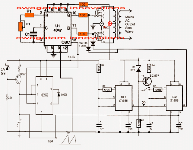
Referring to the below shown IC 4047 pure sine wave inverer circuit (designed by me), we can see two identical IC 555 stages, wherein the left section functions as a current controlled sawtooth generator while the right hand side section as a current controlled PWM generator.
The triggering of both the 555 ICs are derived from the oscillator output readily available across pin#13 of IC 4047. This frequency would be 100Hz if the inverter is intended for 50Hz operations, and 120Hz for 60Hz applications.
Using IC 555 for the PWM Generation
The left 555 section generates a constant sawtooth wave across its capacitor which is fed to the modulating input of the IC2 555 where this sawtooth signal is compared with the high frequency signal from pin3 of IC1 555 creating the required pure sine wave equivalent PWM at pin#3 of 555 IC2.
The above PWM is directly applied to the gates of the mosfets. so that the square pulses here generated through pin10/11 of IC4047 gets chopped and "carved" as per the applied PWMs.
The resulting output to the transformer also causes a pure sine wave to be stepped up at the mains AC secondary output of the transformer.
The formula for calculating R1, C1 is given in this article which also tells us about the pinout details of the IC 4047
For the NE555 stage C may be selected near 1uF and R as 1K.

Assumed output waveform
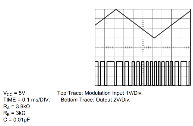
More info on how to use IC 555 for generating PWM
An RMS adjustment could be added to the above design by introducing a pot voltage divider network across pin5 and the triangle source input, as shown below, the design also includes buffer transistors for improving mosfet behavior
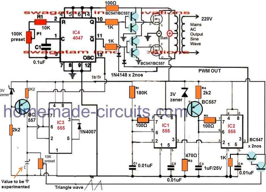
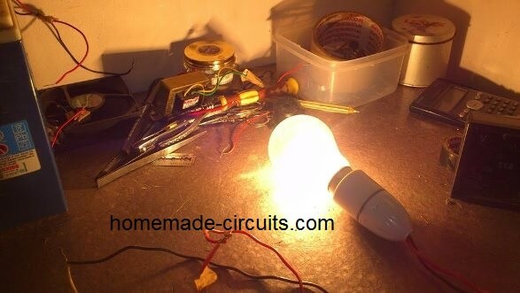
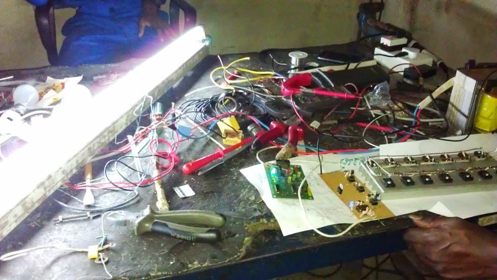
The above pure sine wave inverter design was successfully tested by Mr. Arun Dev, who is one of the avid readers of this blog and an intense electronic hobbyist. The following images sent by him prove his efforts for the same.
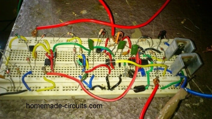
More Feedback
Inspiring response received from Mr. Arun regarding the above IC 4047 inverter results:
After completing this circuit, the result was amazing. I got full wattage by the 100 W bulb. Couldn't believe my eyes.
The only difference i had made in this design was replacing the 180 K in the second 555 with a 220 K pot to adjust the frequencies accurately.
This time the result was fruitful in all respects... On adjusting the pot, i could get a non disturbing non flickering full wattage glow in the bulb, also the 230/15 V transformer connected as the load gave a frequency in between 50 and 60 ( say 52 Hz ).
The pot was adjusted gently to get a high frequency ( say 2 Khz ) output from pin#3 of second ic 555. The CD4047 section better calibrated to get 52 Hz at the two output terminals....
Also I am facing a simple problem. I have used IRF3205 mosfets at the output stage. I forgot to connect the safety diodes across the drain terminals of each mosfets...
So when I had tried connecting an another load ( say table fan ) in parallel to the given load ( 100 W bulb ), the glow of the bulb also the speed of the fan was reduced a little and one of the MOSFET was blown due to the absence of the diode.
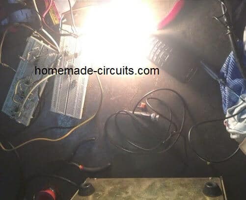
The above 4047 sine wave inverter circuit was also tried successfully by Mr. Daniel Adusie (biannz), who is a regular visitor of this blog, and a hardworking electronic enthusiast. Here are the images sent by him verifying the results:
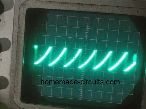
Sawtooth Waveform Oscilloscope Output
Illuminating a 100 Watt Test Bulb
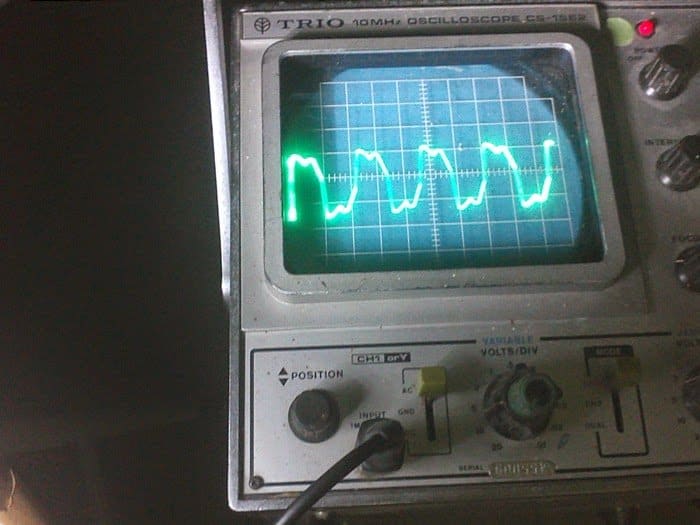
The following images show the modified waveforms at the output of the transformer as captured by Mr. Daniel Adusie after connecting a 0.22uF/400V capacitor and a suitable load.
The waveforms are somewhat trapezoidal and are far better than a square wave which clearly shows the impressive effects of the PWM processing created by the IC555 stages.
The waveforms could be probably even further smoothened by adding an inductor along with the capacitor.
Showing an near Sinewave Oscilloscope Trace after PWM Filtration
Interesting feedback received from Mr. Johnson Isaac who is one of the dedicated readers of this blog:
Good day
In your post, Pure Sine Wave Inverter using 4047, in the second I.c stage (ic.1) you used 100 ohms resistor in between pin 7 and 6.,
Is that correct? I use to think an astable multivibrator using 555 pin configuration should have the 100 ohms between pin 7 and 6. Also, the 180k variable between pin 8(+) and pin 7. Pls check the pin connection and correct me pls. Because it oscillate sometimes and it doesn't sometimes also. Thanks,
Isaac Johnson
Solving the Circuit Issue:
In my opinion, for a better response you can try connecting an additional 1k resistor across the 100 ohm outer end and pin6/2 of IC1
Johnson:
Thank you very much for your response. I actually constructed the inverter you gave in your blog and it worked.
Though I don't have an oscilloscope to observe the output waveform BUT I bet readers its a good one cos it operated a fluorescent tube lamp in which any modified or pwm inverter can't power on.
See the picture sir. But my challenge now is when I add load, the output flickers sometimes. But am happy its a sine wave.
Video Test Waveform
Simplifying the above Concept
The above explained IC 4047 pure sine wave inverter can be actually simplified greatly by eliminating two IC 555 configurations from the design.
The basic idea is to produce a synchronized sine PWM output for chopping the MOSFET switching so that this SPWM waveform is replicated at the output of the transformer and is transformed into a pure sine waveform. The complete circuit diagram can be seen in the following diagram:
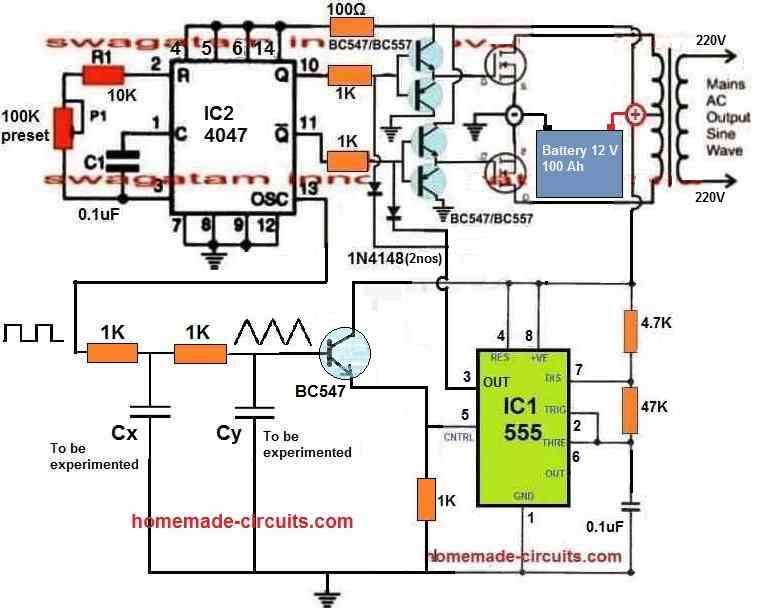
In this simplified design, we yet again exploit the pin#13 square wave output from the IC 4047 and convert it into triangle waves. This triangle wave is then used to modulate the PWM output of a IC 555 astable to create the required synchronized SPWM for chopping the MOSFET gates.
The capacitors Cx and Cy will need to be experimented a bit to create a proper triangle waves from the RC network output.
Remember, you will need an oscilloscope to check and confirm the various waveform discussed in the above diagram.
Another Simpler Looking Options
The following concept discuses a rather simpler method of modifying an ordinary square wave inverter using IC 4047 into a sine wave inverter through PWM technology. The idea was requested by Mr. Philip
Technical Specifications
I hope that i am not going to be a bother, but I need some advice with a PWM-controlled modified sine wave inverter I am designing so I want to seek your expert opinion.
This simple design is tentative, I haven't implemented it yet but I would like you to take a look at it and tell me what you think.
Also I want you to help answer some questions which I have not been able to find answers to.
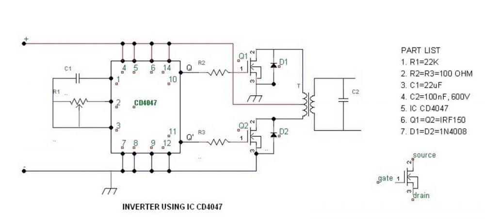
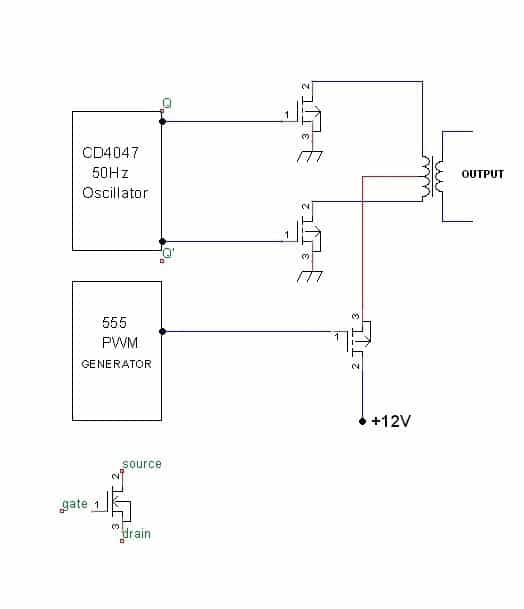
I have taken the liberty of attaching an image of a quasi-block diagram of my tentative design for your consideration.
Please help me out. In the diagram, the IC CD4047 in the inverter is responsible for generating square wave pulses at 50Hz which will be used to alternately switch on MOSFETS Q1 and Q2.
The PWM circuit will be based on IC NE555 and its output will be applied to the gate of Q3 so that Q3 will provide the PWM. Besides this, I have two questions.
First, can I use square waves for the PWM pulses? Second, what is the relationship between PWM frequency and supply frequency? What PWM frequency should I use for a 50Hz inverter output?
I hope that this design is feasible, I think it is feasible, but I want your expert opinion before I commit scarce resources to implement the design.
Looking forward to hearing from you sir!
Sincerely, Philip
Solving the Circuit Request
The configuration shown in the second figure above would work only if the center tap mosfet drain/source pins are swapped and N-channel mosfets are used for the 4047 inverter oscillator output, as shown below:
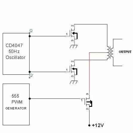
The PWM section should be built as I have explained in this article:
The PWM transforms the flat square waves into a modified square wave by chopping them into smaller calculated sections such that the overall RMS of the waveform becomes as close as possible to an actual sine counterpart, yet maintaining the peak level equal to the actual square wave input. The concept may be learned in details here:
However the above transformation does not help to eliminate the harmonics.
The PWM frequency will be always in the form of chopped square waves.
The PWM frequency is immaterial and may be of any high value, preferably in kHz.
How to Add Feedback Voltage Control to a 4047 IC Inverter
In this section we will discuss how to add an automatic feedback voltage control to a 4047 IC based inverter circuit.
If you don't want to read the whole explanation, you can watch the following video instead:
This type of feedback network is intended to ensure that the AC output voltage from the inverter never exceeds a predetermined safe value. For example, using this automatic feedback control, a 220 Volt inverter circuit output could be restricted to maximum 230V AC level, which may be safe for most 220 Volts appliances.
For a 120 Volt inverter system, this feedback network could be adjusted to restrict the output AC to a maximum of 115 Volts AC, which may be safe for most 110 Volt appliances.
How the Feedback Circuit Works
Now let's understand how the simple feedback network is designed to work, by referring to the following circuit diagram:
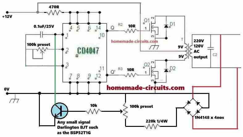
The mains AC voltage from the inverter transformer secondary is first converted to a DC voltage using a bridge rectifier.
This bridge rectifier is built using 4 numbers of 1N4148 diodes.
The DC 220 Volts output from the bridge rectifier is applied to an adjustable voltage divider network built using a 220 k resistor and a 100 k preset or trimpot.
The 100 k preset is carefully adjusted such that its central wiper terminal generates around 1.2 volts in response to an input AC voltage which is considered high, and needs to be restricted.
Let's say, the input AC needs to be restricted at around 270 Volts, then the 100 k preset may be adjusted so that its wiper terminal generates a proportional DC voltage level of 1.2 Volts.
We select a 1.2 Volt output because this is the equivalent DC level required to just switch ON the attached BJT device.
That means, whenever the inverter output AC voltage tries to exceed the 270 Volts mark, it causes the BJT to turn ON and become conductive.
When the BJT conducts, it starts grounding the CT pin of the IC 4047.
Since the RC network associated with the CT and the RT pinouts of the IC determines the output frequency and PWM, the grounding of the CT pin instantly causes the output PWM and frequency to nullify, which in turn causes the output AC voltage to dip.
When this happens, the feedback voltage to the BJT also drops proportionately until the BJT is turned off. In this situation the IC output PWM is restored back to its previous form, and if the output voltage continues to rise, it yet again activates the BJT via the feedback network, and this feedback on off cycle keeps repeating rapidly, ensuring that the output AC is not able to rise above the set threshold, which is 270 volts in our example.
This concludes our feedback control circuit explanation, now let's try to understand how this feedback circuit can be setup prior to integrating it with the inverter circuit.
How to Setup
The next diagram below shows the isolated feedback circuit, which can be set up by implementing the following steps, before interfacing it with your inverter circuit:
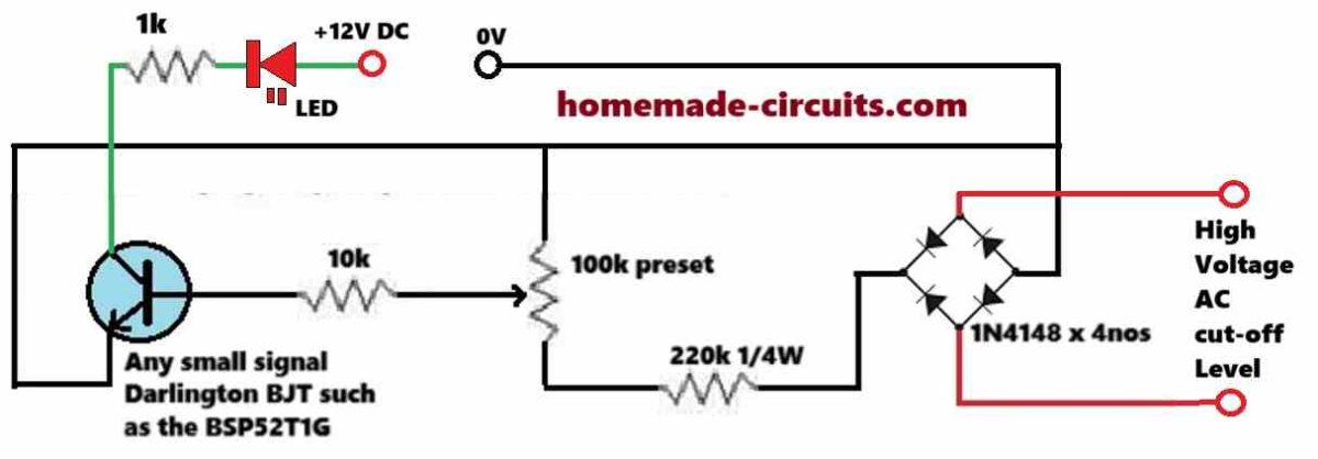
Initially keep the 100k preset's wiper arm fully towards the ground side of the DC supply.
Now, switch ON the 12 DC supply and then switch ON the AC supply to the bridge rectifier whose voltage level is around the desired high cut-off limit.
Next, slowly adjust the preset using a well insulated screw driver, until the LED just begins to illuminate.
To confirm the results, try varying the input AC voltage around the cut-off threshold and watch the LED turn on and off at the thresholds. Although the cut-off may not be too sharp, yet it will do the job of the intended output voltage control of the inverter quite well.
That's it! This simple procedure should be enough to complete the setting up of the feedback circuit.
After this, make sure to seal the preset adjustment with some super glue.
So, this concludes our explanation on a feedback circuit for the 4047 inverter.
Pseudo-sinusoidal IC 4047 Inverter Circuit
From a continuous source, battery, or vehicle alternator, it is possible to produce a 50 Hz voltage/pseudo-sinusoidal waveform, using this simple IC 4047 inverter circuit. The design is capable of operating many low-power devices that require a voltage of 220 V AC, typically supplied by the AC mains grid distribution network. The power of this module depends largely on the chosen transformer and, above all, on the continuous source's ability to supply the circuit without failure.
Working Principle of the circuit
Being able to power a device on the 220 V AC network when no mains AC power is available can be very convenient. We particularly think of campers, caravanners, fishermen, and motorists.
Although this simple setup does not provide a 100% clean sinusoidal wave, it can still satisfy many undemanding devices such as incandescent or fluorescent lighting, soldering irons, small motors, etc.
The power can reach up to 250 VA if the continuous source is strong enough and an adequate toroidal power transformer is chosen.
The power transistors are rated for 30 A, provided that a substantial heatsink is used.
We even suggest adding a small fan directly connected to the 220V output, which will prevent it from operating without a load.
Analysis of the Circuit Diagram
To obtain an alternating voltage from a DC source, the simplest solution is to use an inverted transformer: the low-voltage secondary winding has a center tap.
It is then sufficient to alternately supply power to the two windings to produce a symmetrical, but non-sinusoidal, variable voltage on the primary side if the low-voltage secondary winding is driven by a rectangular signal with steep edges.
Two complementary and opposite signals are required, and the CMOS integrated circuit with the reference 4047 is used to generate them, capable of either building an astable or monostable flip-flop.
The proposed diagram is shown in the figure below.
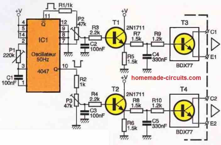
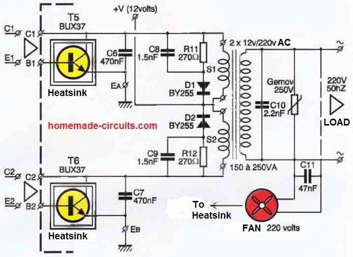
Of course, we will operate our circuit as an astable generator, ensuring a precise frequency of 50 Hz. This task is entrusted to components C1 and P1. Some pins of the IC1 circuit are connected to the ground or the positive supply, depending on our needs.
For more information, you will find an explanation in the appendix about the multiple possibilities of this practical little integrated circuit.
The symmetrical square voltages available at pins Q and Qdash (corresponding to terminals 10 and 11 of the circuit) are routed through resistors R1 and R2 to an adjustable element. Its role is to balance the amplitude of the two signals and facilitate the adjustment of the control module.
Note that the duty cycle will be exactly 50% by design. The sliders of elements P2 and P3 control the base of a 2N1711 transistor, which is responsible for driving the downstream power semiconductors.
Components R7, R9, C4, as well as R8, R16, and C5, form a coarse filter capable of smoothing out the signal angles to some extent.
This will allow us to create a "pseudo-sinusoidal" signal that will control the intermediate transistors T3 and T4 mounted on the small control board.
The BDX 77 models are rated for an emitter-collector voltage of 80V and a maximum peak current of 8A. They are delivered in a TO-220 package and will benefit from a heatsink.
The secondary windings of the transformer do have a common point connected to the positive pole of the power supply.
The other end of the coils will receive the ground through the power transistors T5 and T6, a model not much larger than the famous 2N3055 but with a maximum peak current of around 30A in this case.
It is the NPN bipolar model with the reference BUX 39.
Diodes D1 and D2 absorb the unavoidable breakdown current produced at each interruption of the inductive element, which is the transformer.
The primary of the transformer, a toroidal model in this case, delivers a 50 Hz AC voltage.
The component labeled Gemov (or varistor) is placed between the output pins to clamp excessive voltage surges that may occur.
Two wires can also be tapped from the output to operate a fan directly powered by 220V, which will provide airflow to cool the transistor-heatsink assembly.
It is important to ensure that the voltage of the continuous source does not drop too much or be completely depleted in the case of a lead-acid battery.
It goes without saying that the input DC current can reach considerable values if, for example, a power of 200VA is desired. It would be prudent to include a robust series fuse, similar to those found in a household installation.
Construction
The creation of two printed circuit boards is necessary: the first one, shown in the figure below, is designed for the components described in the control module.
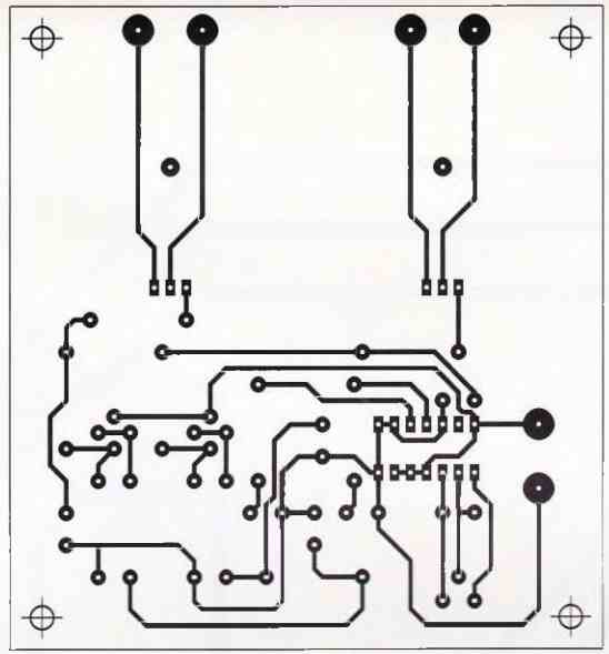
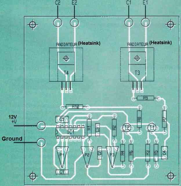
The layout is not very dense, but it is still recommended to use pre-sensitized copper-clad boards for reproduction.
After etching and rinsing, various drillings are carried out. Care must be taken to carefully mount transistors T3 and T4 on a small heatsink, which is directly attached to the epoxy board.
From this board, six wires will go to the significantly larger power module, and the track layout at a 1:1 scale can be found in the figure below.
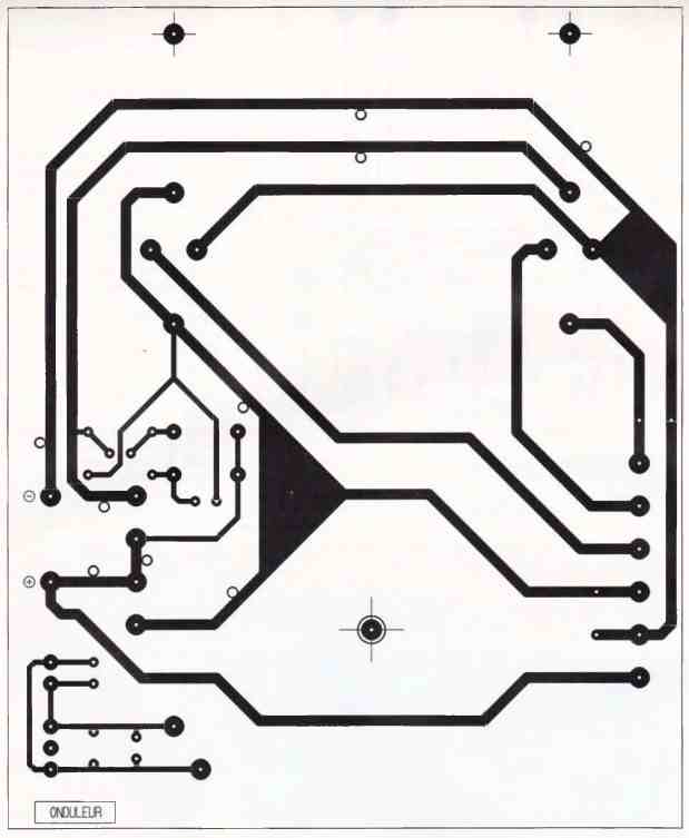
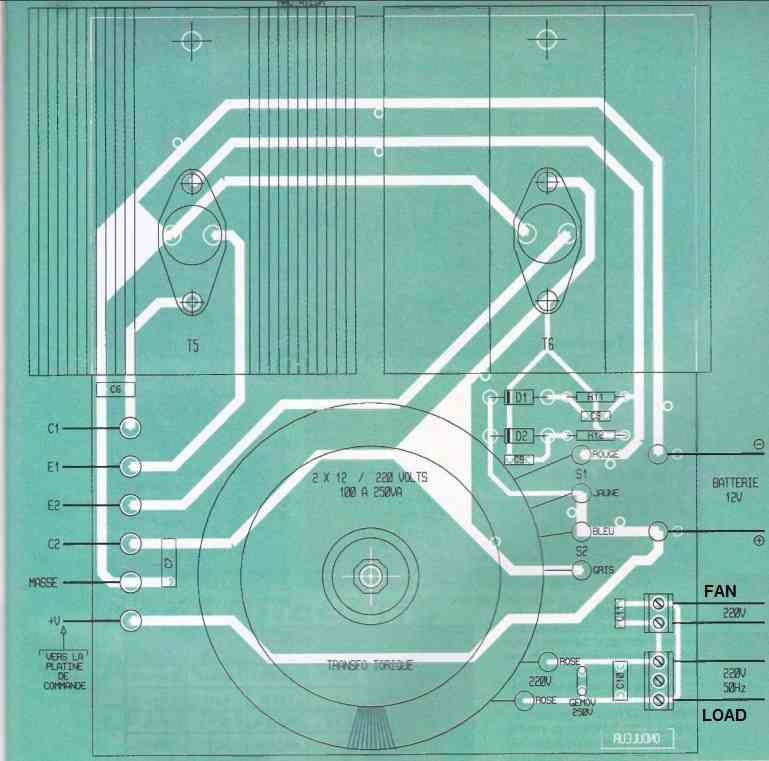
It should be noted that certain tracks on this simple IC 4047 inverter circuit board will carry high currents and require special treatment. We recommend soldering bare copper lengths, with a section of approximately 1.5 mm2, directly onto these tracks.
For example, electrician's copper wire with the insulation removed can be used. Care should also be taken to ensure all connections between the two boards, and in particular, to avoid reversing the wires.
The transformer has six wires, with the two thinnest wires corresponding to the primary, and therefore our 220V output.
It is important to properly identify the other windings before soldering them permanently. This assembly can be housed in a sturdy, adequately ventilated metal enclosure.
How to Setup
We leave it to you to complete this final step for this simple IC 4047 inverter circuit. After a thorough check, the frequency can be adjusted to 50 Hz under no-load conditions using the adjustable preset P1, if you have an oscilloscope or frequency meter.
Otherwise, simply set this element to the midpoint position. The other two adjustable components are set to obtain a symmetrical signal in amplitude.
Initial tests can be performed using a simple socket where different power lamps can be connected. For resistive or slightly inductive loads, there should be no serious issues.
Proceed with caution when testing devices that typically require a true sinusoidal voltage.

to the far left 555ic is the zener diode 27v or 2.7v?
and the resistor below it is it 2.2k or 22k?
can I get r1, c1 and p1 values
what can I use to replace bc557 I am only getting replacement parts to buy.
and I can only get ne555 not (7)555 can I use 3 ne555
2.7V zener and 2.2k resistor
r1,C1, P1 will need to be adjusted by practical monitoring for the required vrequency
any low power PNP will do for BC557
any 555 IC will do
if i am using a 12 volt battery source to this circuit my transformer would have to be a 6v centre tap? but since the ic can only manage 15v then adding a source voltage over that would require a regulator to limit it to probably under 16v so wouldnt that just allow the use of a 6-0-6 transformer.
the ICs can be powered from the battery itself…
the trafo is directly connected to the batt via the mosfets, not the IC
Thanks for the quick responds. Engineer I want to know if I want to add a driver stage where will i put it and what values will be best. I add a driver to the circuit with bc547 as transistor and 1k as the gate resistor from the ic. What i observe is that one side of the fets was heating. When i remove the fets and drive the fets directily there was no heating. all the test was done with no load connected. When i check the voltage from bc547 it was almost as high as the battery voltage and when i remove it and check the voltage from the ic it was around 4,2v, The reason for the driver was that i want to add more transistors and use a bigger transformer.
kinnajingo, please refer to the following design for your required application:
1.bp.blogspot.com/-NgqlieM8TX8/U7zL0tGH6qI/AAAAAAAAHgE/WCKLVG9pVVs/s1600/mosfet+transistor+driver+circuit.png
accross the output of this circuit could an inductor be placed to filter wave form if so what value could I use?
I see 2 schematics is the one without the 1n4148 diodes at the gate of the FETS the modified version?
what is the value of P1 connected to the 4047 ic?
You can try the third last circuit provided in this aticle:
https://www.homemade-circuits.com/2013/10/modified-sine-wave-inverter-circuit.html
P1 in the above circuits is for adjusting the 4047 output to the desired frequency level.
Mr Swagatam I found this on the blog for 4047 ic frequency calculation
f = 1/8.8RC at pin10 and 11
Where f is in Hz, R in Ohms and C in Farads.
Engineer correct me if we choose the values Odon pick thus P1+R1 =22k and C1 = 0.22uf and calculate for frequency. I got this 8.8*22000*0.22uf=42592 but since 0.22 is in uf i divided the result by 1million to get the farad f. So 42592 divided by 1m =0.042592
Now for frequency 1/0.042592=23hz If this is true then the actual f is not even 50hz.
please sir correct me if am wrong.
Mr.kinnajingo, the best and the simplest way to confirm it is by connecting a frequency meter across the relevant pins of the IC..
Your formula and calculations may be correct but the final confirmation will need to be done using a frequency meter.
Thank you Engineer for your help, but please can you help with the value for R1+P1 and C1 because i don't understand how they came by the 50hz frequency. Is there a mathematical formular for this?
hi sir, Can the Atmel 89S2051 chip be used to create a pure sine wave inverter?
sorry randy I don't have much info regarding this…
Hello, sir:
I would like to have it output 5Vac and 10 Vac. How do I make that happen?
Thank you!
hello phil,
use a transformer having the secondary winding specified with 5VAC or 10V AC rating
Hello, sir:
I don't understand how transformers work very well, so please forgive me if this is a dumb question. My Vin is 12 Vdc, so should I get a transformer that has the Voltage input of ~12 volts? Also, I found out that most transformers have 6 and 12 Vout. I can't find transformers that have 5 and 10 Vout. Could you briefly how this works? Thank you!
Hello phil, if your AC requirement is not bipolar meaning alternating from positive to negative and vice versa then probably you wouldn't require a transformer at all, but if it's bipolar then you would require a trafo as mentioned in your comment itself….primary should be rated with 12-0-12 and the secondary with 5-0-5v….you may have to get it designed specially from a transformer maker..
Hello, Mr. :
I'm having trouble finding BC 557. Can I use any kind of PNP transistor?
Any general purpose PNP BJT will work…
Thank you so much.
May I have one more last question? If I don't use a transformer and my Vin is 12 Volts DC, then what would the output Vac be? would it be 12 V AC?
it would be a pulsating 12V DC, not a bipolar 12 VAC
Hello sir, i have tested this circuit on bread board. this is awesome. Can you give me its pcb layout please
Hello Micky, thanks very much, however due to time constraint making the layout won't be possible at the moment for me…
Dear Mr. Swagatam Majumdar,
Thank your for the circuit design schematic & breadboard pictures. Although difficult (for me), I enjoyed putting this together. I put together the last schematic on this page, with the BC547 included for parallel mosfets. It works nicely for me.
I have not yet added parallel mosfets.
I think my previous attempt to reply did not post because I had not logged in, so I will try this again.
For the benefit of others, I wanted to mention that I had a few problems, mostly regarding having the wrong parts, and selecting the wrong values per the schematics. It took me a while to get it completed correctly.
Let me see, I would guess that my biggest problem was with the capacitor and resistor at C1 and R1 of the 4047. I had to study the comments from the breadboard pictures in order to get that correctly. I had missed the period from other schematics, and had guessed at 22 uF (for C1). That was not correct, as it gave me a pulsed flash in about every second.
For C1, I have tried .01uF and .22uF, both of which work for me. I am currently runing from .22uF, rated at 630 volts, per the comments regarding the successful breadboard trials.
For R1, I am currently running with 22K Ohms, without P1 on the 4047. This works for me, but I suspect that I need to adjust the frequency in some systematic fashion.
I do not have a oscilliscope, and I am in the U.S., so I have looked at the equations for frequency from some of your other posts. I suspect that I will buy an oscilliscope in order to check the frequency.
I had ordered 2.7 volt Zener diodes, but when they arrived, I found that I had ordered 1/2 watt zeners, and not 1/4 watt zeners. The 1/2 watt zener diodes gave some slight flickering, so for the moment, I am using 1N4148 diodes. I will order the zener diodes again.
I am currently running from three NE555's. I had bought 7555's from Radio Shack, but removed them to trouble shoot my problems.
Finally, I have some small concern regarding the breadboard comments about the burned out mosfet, due to no protecting diodes. My front mosfet gets hot quickly, and I do not see the protective diodes surrounding the mosfets in the schematic at the bottom (with the 547 addition).
I am running with IRFP150 mosfests, as I am having difficulty finding IRF150 mosfets. I also have IRF3105 mosfets, but am not currently using the 3205's.
I think that the capacitor at C1 was my biggest problem there.
Thank you very much. Although difficult (for me), I got a thrill from seeing it work!
– Dave Hamm
Thanks Dave, for the great explanation!
Yes an oscilloscope will be quite handy for checking the overall response of the system, and would also allow you to study the output waveform.
In the meantime you could try varying the lower 10k preset and see if the output voltage also varies correspondingly, this will prove that the PWM section is working correctly as proposed in the article.
Thanks for the response.
Yes, I did look at the 10K preset. I had done the calculations from your web page on "IC 4047 Datasheet, Pinouts, Application Notes" and calculated that P1+R1 should equal about 55 MHz when C1 is 0.22uF
However, I have very little confidence in my understanding of your equations.
I noticed a clue about the frequency when I had C1=0.22uF and R1+P1 = 22K. My little test 1 watt night light would give a humming sound that was quite noticeable.
So, yes, I did place a 10K resistor in for P1+R1, leaving C1 at 0.22uF, and the humming sound of the night light went away as soon as the 10K (preset) was in place.
Also, while using the 10K resistor in place for R1+P1, I did a test of a light load, a 15 Watt incandescent and let it run for about 45 minutes. During that time, the front mosfet (the lower one on your schematic) did not heat up hardly at all.
Therefore, at first glance, it would appear that the 10K preset is much better than the 22K which I was initially using (while using C1 is at 0.22uF). I will leave it at the 10K until the oscilloscope arrives.
On a side note, it also appears to be very energy efficient, which came as a pleasant surprise to me. I don't know the figures for efficiency, but it appears to have less drain on the batteries than I would have normally expected.
Just wonderful to see it working.
Thank you
Thanks Dave, actually I was referring to the lower 10K preset associated wit the first 555 IC from left.
It's included for facilitating RMS adjustment or the average output voltage of the circuit.
Regards
Thank you dear Odon,
I am very happy and excited to see the results…
However I may have to delete this comment since you have posted your personal blog link, which I cannot publish.
If possible please post the comment without this link and I'll make sure all the info gets published in the above article.
Sir can i ask your help. Can you give me a circuit of pure sine wave inverter that is atleast 300 or 500 watts 12v-220v dc-ac inverter 50-60 hz that is easy to build.
Hope you will aswer.
Thanks…
you can convert any small inverter circuit into a high power inverter circuit by following the instructions provided in the following article:
https://www.homemade-circuits.com/2014/10/upgrading-low-power-inverter-to-high.html
sine wave can be accomplished as explained in the above 4047 inverter article
sir please you did not upload the circuit im still waiting for it
daniel, please draw the schematic as per my previous instructions and send it to me, I'll check it for you and confirm its accuracy or make the necessary corrections in there are faults.
sir please im still waiting for the update please sir you promised to update we are still waiting for it thank you.
daniel, please draw the schematic as per my previous instructions and send it to me, I'll check it for you and confirm its accuracy or make the necessary corrections in there are faults.
here are the instructions:
we have 6 NOT gates inside a 4049 package
connect the inputs of three NOT gates in parallel meaning join them together, connect this joint to one of the outputs of the 4047 IC VIA A 1K RESISTOR.
Now connect the individual outputs of these gates to three separate mosfets via 100 ohm resistors.
join all the drains of these mosfets to one of the outer taps of the trafo.
Repeat the above procedure for the other three NOT gates and configure them with the other output of the 4047 IC and the trafo tap.
After completing the above you can integrate the PWM input at the junctions of the NOT gates and 1K from the 4047 outputs.
sir please i did as you said but it didn't work i think the corrections are wrong connected so can you please update it thank you looking forward to hear from you .
daniel, please draw the schematic as per my previous instructions and send it to me, I'll check it for you and confirm its accuracy or make the necessary corrections in there are faults.
sir
please as im talking to im on it but it didn't work maybe the connections are wrong connected sir i tried to send you the diagram but we are having a problem with our network so please can you try to update it for me?thank you.
ok sir
im still waiting for the update thank you
daniel you can do the following steps:
we have 6 NOT gates inside a 4049 package
connect the inputs of three NOT gates in parallel meaning join them together, connect this joint to one of the outputs of the 4047 IC VIA A 1K RESISTOR.
Now connect the individual outputs of these gates to three separate mosfets via 100 ohm resistors.
join all the drains of these mosfets to one of the outer taps of the trafo.
Repeat the above procedure for the other three NOT gates and configure them with the other output of the 4047 IC and the trafo tap.
After completing the above you can integrate the PWM input at the junctions of the NOT gates and 1K from the 4047 outputs.
don't forget to connect the 4049 supply pins to the supply from the battery otherwise the IC will not work
hi sir
please i finally build this circuit but still big problem i used four fets two at one side and two at other side so total four,if i power the circuit the fets got very hots if i set the frequency to 50HZ it got hot and if set up to 60HZ the same problem i change all the 555 and cd4047 please i now i need your assist thank you.
Hi Daniel in that case you can revert to the previous concept and use the PWMs on the mosfet gates.
for adding more mosfets you can use 4049 NOT gates and terminate their outputs with mosfets.
I'll try to update the idea soon…
ok sir thank you for your kindness
thank you sir
it st going to produce same wave form?
I hope so, it will need to be confirmed practically
ok sir
im waiting for it thank you
done! please check it out.
ok sir
i did it but it didn't work i don't know maybe wrong connection,please make the diagram and update it for me cos i want to make a bigger to see if this inverter is good for my need thank you sir hope to hear from you son.
daniel, I 'll try to update it soon….may be tomorrow.
ok sir
please im confused sir cos you said should connect to positive i don't understand the word via it is (with) or what? 10k resistor please can you update it for me co what you said confuted me
via means "through", meaning the mentioned connections must not be joined directly to the respective points, rather they must be connected in series with the mentioned resistors.
if possible i'll make the diagram and update it
sir
i want to add more fet how do connect 1n4148 diode for example if i want to add 10 most fets every each of them should connect with 1n4148 diode?
daniel,
instead of using the mosfet gates for pwm control, it's better to use pin9 of the IC 4047 for applying the pwms, ……do the following:
first disconnect pin9 from ground and connect it to positive via a 10k resistor.
take a BC547 transistor and connect its colector to pin9, emitter to ground and base to pin3 of IC2 (555) via a 10k resistor…diodes are no longer required.
now your mosfet section is free so that you can connect as many of them in parallel.
make sure the gate of each mosfet has its own 100 ohm resistor and also put a 1k resistor across each mosfets gate and source.
sir please it good to get 70HZ out put? cos when i set it to 50hz the more i load the more it going up it not stable,please sir if i want to connect inductor where it should be connect ,sir can this circuit handle 24v dc batt and how to connect it thank you sir.
biannz, 70Hz is not good.
use 7809 IC for supplying the 555/4047 IC positives from the battery.
once you do the above, you can use 24V also without worry. use the 24v battery in the same position where presently the 12V is.
Sir,
Have u deleted the Pure sine wave inverter using Traic from your blog ?
Are you in the middle of making a correct working model ???
Arun, yes I have deleted the article temporarily, but there's no easy way of switching the output with the PWM unless a full bridge driver circuit is used at the output as shown below:
https://www.homemade-circuits.com/2014/01/simplest-full-bridge-inverter-circuit.html
ok sir please you said that inductor can be use so im asking you that where it should be connect and how many turns, this wave form is (2ms and 5 volt/DIV) sir i think i have succeed in this circuit so what i need is low battery cut off so sir can you please design one for me? thank you.
one filter circuit is shown in the following circuit you can try it out:
https://www.homemade-circuits.com/2013/10/modified-sine-wave-inverter-circuit.html
for the low battery cut off you can try the folowing design:
4.bp.blogspot.com/-r70Wh0qXC78/U18yct62aFI/AAAAAAAAGws/gx2FCQRc5e8/s1600/automatic+battery+charger+circuit.png
use the lower free relay contact(N/O) for connecting with the inverter positive.
ok sir thank you,so you mean this wave form is alright?but you said that it equivalent sine wave not modified sine wave cos modified sine wave don't look like this or? ok sir help me with this if i connect 220v fan it run very good but if add another load like 60w bulb the voltage reduce so the fan stop.
yes this wave looks alright since it's the outcome or the resultant of the PWMs applied at the primary.
The transformer is not able to support higher loads because its winding may not be rated to handle that much load…..use thicker wire for the secondary…and/or increase the AH rating of the battery.
The power handling capacity is not anyway related to waveform or PWM of the circuit.
ok sir thank you sir please check the wave form i sent it to your email address homemadecircuits@gmail.com sir i think it shouldn't be like this any help? so that i can get the wave form correct with this wave form it handle small 220v a/c fan the speed of the fan is ok but the moment connect another load the fan stop waking i use 200ah 12v batt with 9-0-9 transf.
Biannz, it looks very impressive, but please let me know how you got these waveforms, for additions did you do for getting such waveforms.
did you connect a 0.22/400V capacitor at the output, and is the RMS = 220V???
You cannot get better waveform than this, because it's a modified sine wave so please don't expect to get a real sinusoidal type waveform.
Also you may try increasing the output capacitor to 0.33uF/400V and check the response.
I would be publishing the waveforms in the above article so that others can also visualize it.
ok sir,please sir if i connect the diode where the black mack is to the pin 6 and 7 of ic ne555 the sine wave work but it cannot adjust the RMS to get out put 220v A/C but if connect it as it is the sine wave don't work sir all i mean is that the 10k pot cannot be adjust the RMS if the 1n4007 diode is connected,
when the capacitor C charges, the slow rise in the voltage will pass through the diode and go to pin5 of the 555 via the pot adjustment, so I cannot see any reason how the diode can stop this from happening.
check your diode polarity or may be it's faulty.
Anyway if you don't want the diode you can remove it and use the 10k preset directly in the shown position.
Could you please suggest a circuit for enabling the connection from high power output voltage from the inverter to the laptop MIC socket ?
Since i am not so much confident about myself for making such a design to be used with my laptop i am seeking for your help
Try an online "voltage divider software" and select R1/R2/input prarameters appropriately for getting the 1V output.
After this you can make this configuration for acquiring the 1V output
Sir can you suggest any method to identify a sine wave and square wave generated by a circuit separately without using any graphical means such as OSCILLOSCOPE TRACES ??
Arun download "goldwave" free version in your PC, and then you can use this software for monitoring the waveforms on your PC screen,
But remember the input signals will need to be first converted to 1V PP before feeding your PC MIC socket..
ok sir thank you sir please take a look at this if it good to get this voltage at the pins,sir in the ic2 i got 9.31v at pin3 and ic1 i got 6.0 v at pin13 so sir it good?
it looks OK, but now adjust the 10K RMS pot, it should proportionately vary the pin5 average voltage and also the inverter output voltage.
I have tested the circuit with replacing the 10 uf capacitor with other capacitors also…. but the result was same…. The interesting thing noted that, when i am connecting larger capacitors ( say 470 uf/25 V as is found in many ordinary rectification stages ) the produced DC voltage is getting increased slightly from a low value ( say 2.8 V ) to its maximum…
the above modification in the diagram will solve the issue.
Sir
The circuit has been set up initially as a separate testing mode, not incorporating inverter output. The input 230 AC voltage ( under which the inverter output has to become stable ) is given directly as in your circuit… THat 230 V has been taken from the normal house wall socket..
All the circuit components were placed as is on the given circuit… I have not connected the output of the circuit ( transistor collector through the diodes ) to any point.. It is kept free.
But i am getting wrong results even before connecting the transistor stage…. When i am connecting the pot as said before or connecting the 1 K resistance the changes in voltage are very discouraging ones…. I will send the complete pictures to your mail.. Dn't 4get to check it soon…
Arun, I have modified the supply terminals of the diagram a bit, you can check it out here, please do it accordingly:
https://www.homemade-circuits.com/2014/01/automatic-output-voltage-regulator.html
The connection was correct…. Center of the pot to pin#3 of OPAMP other terminals respectively to Sensing voltage and ground…
It z not the problem due to any wrong connections… Then why it is happening the same by connecting the 1 K resistance between the Supply voltage and pin#2 ?
where did you connect the output of the opamp, or the transistor collector through the diodes.
I really don't know how and where you have used the circuit, so please give all the possible details.
But.. the initially i have tested the circuit with the AC from wall outlet ( which is constant 230 V )…
So what variation to have occurred there ?
I have said that, the supply voltage is getting reduced to a low value ( say 2.5 V ) by connecting the pot or the resistor at pin #2 at this constant ac voltage…
How it is possible for the OPAMP to work properly at this low voltage ??
It has been also noted that the supply voltage reduction is less ( say 4.6 V from 6.0 V ) on connecting a 10 K resistor to pin#2 instead of 1K….
but i am fed up with that 10 K pot.
Arun, I think you have connected the preset wrongly otherwise there's no possibility of this happening.
the center lead must go to the relevant pin of the opamp.
you seem to get fed up without investigating the fault
What is the problem behind reduction in the Supply voltage in the automatic regulator circuit when that 10 K pot is being used ?
I have tried using preset as well as volume control, different valued resistances.. but nothing changed…. still the 15 V supply voltage is getting reduced to about 6 V initially connecting the pot. Further reduced on tweaking the pot… So supply to the IC becomes variable. Some times reaches 3.5 V..
The supply is getting reduced to 3.0 V even on connecting the 1 K resistance to pin#2…
I will send you the video to your email… plz check it soon
Arun, please tell me what is the logic behind measuring the supply voltage of the opamp.
You should measure and check whether the output mains is getting controlled or not.
By the way the opamp supply voltage will get proportionately reduced if the output mains gets reduced because the voltage divider input is derived from the mains, so it means the circuit is working.
ok sir thank you but sir i forgot to ask you something that confused me, in the 555 stage on your left hand side there's resister connect to the base of bc557 is it 2k2 or 27k cos i can see it well and sir this is very important question i need you to answer it for me in the 555 stage on your rite hand there's 1uf capacitor non-polar can i use electrolytic capacitor like 1uf/25v or 1uf/35v tantalum? cos 1uf non p is difficult to get it here sir,thank you.
biannz, the resistor is 2.2K or 2k2, the capacitor can be any polarized type such as electrolytic or tantalum.
Sir.. Now the problem has been cleared. I got the real output of this circuit … Now the voltage at gate terminals are not getting reduced as before, thereby getting the same power output under PWM ( very small deviation can be found )…. Frequency at the gate terminals is showing 260 Hz something… The output frequency of the inverter ( found by using a secondary transformer ) was also found to be in the range of 50 to 60 Hz…. The bulb as well as the fan both worked perfectly.
But two small problems remains unsolved;
1). While a load is working, disturbing humming noise is heard ( especially when fan rotates )..
So could it be possible to eliminate these harmonics completely by a second order low pass filter like this…
4.bp.blogspot.com/-o0KcHSbQKlE/UsQmcGY3NzI/AAAAAAAAGE0/LhlxgAGj7vM/s1600/inverter+sinewave+filer+circuit.png
Will there be reduction in inverter power if any of the filter is added at the output ?
2).. The output voltage is still above 300V.. I have tried the simple opamp output voltage regulator..
4.bp.blogspot.com/-9OIstOS8aAU/UsUgRWbQoQI/AAAAAAAAGFE/ZtvuDjK8-XE/s320/inverter+load+correction+circuit.png
But the problem is that the transistor collector terminal is showing no voltage when the opamp output goes high.. I have checked the circuit separately ( without connecting to the gate terminals of the MOSFETs )……checked removing the zener diode to the base and connecting the 10 K resistor directly….but no response.. Pin#2 shows the correct reference voltage of about 5.0 V… I could also change the voltage at pin#3 using the 10 K pot, also got the output pin#6 go high at a point.
For knowing whether the transistor responds to the opamp output voltage or not , i have checked the voltage between collector and the positive supply of the circuit… It always shows a constant voltage ( full supply voltage… No cahnge )
Noted things :
– Ground terminal of this output voltage regulator has been connected to the circuit ground
-The Ac voltage across the 15 K resistance in the Divider networrk is about 14-16 V.
-The Dc voltag created by rectification is also having the nearer magnitudes.
The fact is that when i am connecting the 10 K POT as in the circuit, the AC voltage found across the 15 K resistor is getting reduced to a low value ( say 6.0 V ), so the DC voltage too… Maximum of 6.0 V DC i am getting
Expecting your reply soon.
Arun, If the mosfet gates are not showing a reduced average voltage with the PWM stage connected it means the PWM stage is not working or has been rendered inactive.
For the overload protection circuit the cut off switching at the collector will be so rapid that you won't be able to read the switch OFF time there.
To visualize whether the cut off and self adjusting feature is working or not, just connect an LED in series with the base of the transistor, connect the zener diode also.
Now suppose you have set this circuit to cut off at around 250V, the red LED will switch ON when this level is crossed and the LED will keep glowing as long as the output keeps producing the high voltage.
Actually the LEd and the opamp switching would be oscillating ON/OFF at a very high rate but won't be visible to the eye.
However this rapid ON/OFf switching of the opamp/transistor will make sure that the output voltage is controlled at 250V and not allowed to exceed.
Now if the output drops below the 250V mark, the opamp output will switch OFf and the LED will also shut off indicating a normal or lower voltage from the inverter, below 250V
You must set and test the above things manually first and only after confirming the opamp behavior connect it with the final set up.
thank you sir but my problem is the out put i don't get correct wave form at the transf out put so it could not handle ac fan well i sent you some pic and video please check it for me, i need your help im almost done so please help to succeed thank you homemadecircuits@gmail.com
biannz, connect a 0.22uF/400V capacitor at the output of the trafo and check the waveform…also check by connecting a load to it.
I forgot to ask you one thing.
Will that 220 k, 15 K resistance combination act like a voltage divider instead of a pot ?
I can't think so, since those resistances are placed prior to the rectification stage.. They are exposed to the direct AC. Think it would be better to place after rectification.
yes the resistor values are selected for getting around 14V, you can check it on any online "voltage divider calculator" software.
It doesn't matter whether it's at AC or DC, the voltage divider will produce the calculated voltage across the selected output points.
But yes, while calculating I should have used 310V as the input (peak) since it's this voltage that would be resulting after the half wave rectification, I used 220V as the input which is not correct….for getting 14V from 310V it should 10k instead of 15K
…the ripples will not have any effect of the intended results, according to me.
Sorry Sir… Last comment was a mistake…. Actually i didn't connect the -ve ( ANODE-ANODE ) junction of the BR to the ground, that is why the voltage appeared -ve…. it is due to my carelessness.
Although the Output voltage doesn't respond on tweaking the pot… It remains at its high level…
4.bp.blogspot.com/-5GDTaart2mw/UmYX6r5TyzI/AAAAAAAAFiI/il_1gPepQVQ/s1600/inverter+output+voltage+correction+circuit.png
SO can i use the below given circuit for my application..
4.bp.blogspot.com/-9OIstOS8aAU/UsUgRWbQoQI/AAAAAAAAGFE/ZtvuDjK8-XE/s320/inverter+load+correction+circuit.png
In this circuit how the output voltage is getting stepped down to power the 741 IC ?
The only one diode along with the capacitor acts as the half wave bridge rectifier.
But, Will that resulting voltage not more than the maximum supply voltage of the opamp ?
I can't see any voltage adjustments for the resulting voltage to suit for powering the opamp here..
And also, Will the output voltage be suitable for this operation since it contains ripples compared to the full BR ?
Another problem is;
As i have already said you that i am getting 330 V+AC output voltage..
I have tried the output voltage regulation circuit..
I got 390 V something DC on processing with the BR. Then tweaked the pot and inspected the voltage at collector terminal…
BUT that voltage w.r.to ground was -ve voltages… Tweaking the pot gave variation from -7.0 V to -16.0 V…
The special thing noted is that ; WHEN I AM FEEDBACKING THE OUTPUT VOLTAGE TO THE PWM CONTROL STAGE, THE ANALOG VOLTMETER CONNECTED AT THE OUTPUT TERMINAL IS NOT SHOWING VOLTAGE MORE THAN 20 V….. thereby unable to adjust the output voltage
Sir, new problems are arriving…
In the current prototype i am working with ( using CD4017 ), i can hear a squeezing sound by the inverter transformer when PWM is connected, this didn't effect the 100W bulb, it didn't flicker or show any disturbing effects.
But the case changed when the bulb was replaced by a table fan ( 55 W only ). The fan rotated at maximum power when PWM was not used, but didn't rotate when PWM has been connected…. Then i checked the frequency at the output terminal of the inverter by connecting a 230/12-0-12 500 mA transformer as the load and checking its output frequency… I got around 1500 Hz…. About the same reading was detected at the gate terminal of the MOSFET….. I remember that, once you had told me that, the output frequency of the inverter will be exact 50 Hz even the gate terminals are fired using high frequency PWM waves… So why it is happening like this…
– Does the result means, the gate terminals are not being fed with the real PWM waves ?
– Then why did the bulb glow at that much high frequency ?
Sir in the last comment of mine,answered by you, i had actually asked you about the waves reaching the two secondary terminals of the transformer ( the terminals connected to each MOSFET drain points ), but you have answered for the output winding…. Think you will notice it.
the alternate switching of the winding at the primary via the two mosfets results in a reverse/forward effect at the output winding.
At last by many trial and errors, without using any DSO, i got the maximum power output at the output terminal of the inverter..
But the circuit in which i made success is not this one. That is the PWM controlled 300 W pure sine wave inverter which you had posted in your blog earlier…
3.bp.blogspot.com/-7PTqKTB9Gvk/UmYcnX3OFiI/AAAAAAAAFiU/F0mIzZBOjNo/s1600/inverter+output+voltage+correction+circuit.png
On inspecting this circuit at initial stages, i got gate voltages equal to about 3.0 V ( Average ) only… I have tried many methods to amplify this signal to at least 6.0V to make the MOSFETs conduct to enable maximum power output, as i have told you many times. But all of them failed, have also told you about this.
At last i have studied the pin details of IC4017 in detail and carried out different practical tests on it… Then i could understand that,
the output voltage available from each output pin of CD4017 = 12V * Duty Cycle of the wave
So if i am connecting pin#10 ( corresponding to 25 % duty cycle ) to the reset pin ( Pin #15 ), i will get only a peak to peak voltage of 6 V.. From this, it is clear that seeing 3.0 V average at the output pins of the IC ( pin#2 and #7 )
So i have changed this connection and connected pin#4 ( by trial and error ) to pin #15. Now i got 6.0 V average at the consecutive pins pin#2 and #3.. But the earlier 52 Hz frequency has been increased to a higher value say ( 150 Hz something )….so frequency adjustment was done at the 555 stage which feeds the clock signals to the IC.. the feeding frequency was adjusted to 100 Hz…then i got exact 50 Hz signals at the above stated pins…. The voltage was 6.0 V average on both pins…. Next step was to ensure whether the signals at these pins are appearing in tandem….I have confirmed this by placing two LEDs at these terminals at 1 Hz frequency……. So everything was set up….
Praying the god, connected the transformer and fired the center tap using the 24 V source…… The result was awesome… Full power output at the inverter output…. No such considerable harmonic disturbances were detected.. Only a slight squeezing sound was heard… Then i have connected the PWM stage…. As in the case of the CD4047 inverter in this page, the gate terminal voltage also got reduced initially… But when i have tweaked the pot associated with the second IC555 ( PWM control ), i could make the voltage reach more than 4.0 V average, hence the power too.
So,,, i want to hear the valuable suggestions and corrections from your side to make this strategy into practical..
On measuring the frequency at the gate terminals with PWM connected, i got nearly about 865 Hz. The Power output in the Bulb was stable. It didn't flicker or make any noises… So can i proceed with this pin strategy ?
I will send you shortly, the current design pictures with output.
I am waiting here to hear your suggestions and comments….
With Regards,
Arun
Thanks Arun, that's great news!
I won't be able to comment regarding the 3.0V issue unless it's verified through a scope.
I think the culprit could be the triangle waves which are not equal to the supply voltage, it means even during the high pulses at pin3, the output would be less by 25%, which would sink the gate voltage by that much, so on an average this would be dragging the gate voltage to 3.0V average.
It would be interesting to see what happens if we replace the square wave and the triangle wave positions in the above design…..square from IC1 to pin5 of IC2 and triangle wave to pin2 of IC2
1).Sir If i am not using a PWM stage , What is the real wave form fed to each secondary windings of the transformer other than the null tap ?
Is it a quasi square wave or just a square wave ?
2). Sir if i am using the PWM stage, will the shape of the wave get affected ?
3). Does the wave fed to each winding has -ve and +ve cycles or just a half cycle ?
Could u plz check your hitman inbox ?
Arun, without PWM it will produce square wave without RMS control
2) with PWM on, the shape of the wave cab be controlled to match sine wave RMS and properties.
3) yes the winding switch alternately in opposite directions resulting in +/- cycles at the output.
Sir i have sent you a mail…hitman2008@….
Plz check it out
I'll check it soon, and let you know.
Sir the addition of the PWM controller stage ( 10K Pot ) you have done at present, doesn't change the output voltage of the inverter….. Tweaking the pot doesn't change its value.
Can this circuit be used to correct the Output voltage to 230 V as well as for voltage regulation
4.bp.blogspot.com/-9OIstOS8aAU/UsUgRWbQoQI/AAAAAAAAGFE/ZtvuDjK8-XE/s1600/inverter+load+correction+circuit.png
Arun, yes the linked circuit will surely work, but before that please try the new position of the 10k pot which can be seen in the updated diagram above.
All your readings are perfect, I can't see anything in them.
………….All your readings are perfect, I can't see anything wrong in them.
Sir are these reading OK ?
1). Frequency generated by IC1 pin#3 and fed to IC2 = about 2.2 Khz
2). Frequency generated by CD4047 ( at pin#13 ) = 106 Hz corresponding to two 52 Hz opposite phased square waves at pin#10 and #11.
3). Frequency of the sawtooth wave form from leftmost 555 IC = 106 Hz
4). Frequency output ( across pin#5 capacitor ) of IC2 = 106 Hz, which is the PWM signal
Comparing the High frequency ( say 2.2 Khz ) with the sawtooth frequency ( 106 Hz ) i am getting the low frequency ( 106 Hz ) value as the PWM frequency…
ok sir the wave form is at of ic2 pin 5, i forgot to test transf out put i well test it and send it to you, it very difficult to get 0.22uf/400v cap here only we have is 0.22uf/27v but still the fan could not speed up and there is much noise in the fan when it working thank you.
OK biannz, no problem.
0.22 is a not compulsory value, you can try with any nearby capacitor, but should be rated at 400V..
…..the triangle (sawtooth) waves look perfect and match with the specifications.