A very effective pure sine wave inverter circuit can be made using the IC 4047 and a couple IC 555 together with a few other passive components. I have explained the details below.
The Circuit Concept
In the previous post I explained the main specifications and datasheet of the IC 4047 where I have explained how the IC could be configured into a simple inverter circuit without involving any external oscillator circuit.
In this article we carry on the design a little ahead and learn how it can be enhanced into a pure sine wave inverter circuit using a couple of additional ICs 555 along with the existing IC 4047.
The IC 4047 section remains basically the same and is configured in its normal free running multivibrator mode with its output extended with the mosfet/transformer stage for the required 12V to the AC mains conversion.
How the IC 4047 Functions
The IC 4047 generates the usual square waves to the connected mosfets creating a mains output at the secondary of the transformer which is also in the form of square wave AC.
The integration of the two 555 IC to the above stage completely transforms the output into a pure sine wave AC. The following explanation reveals the secret behind the IC555 functioning for the above.
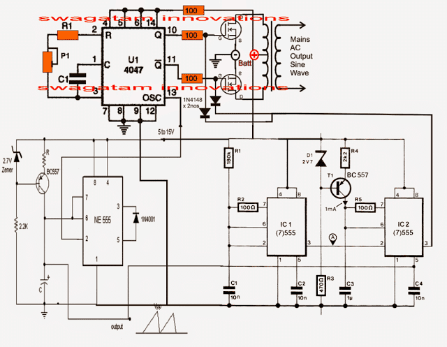
Referring to the below shown IC 4047 pure sine wave inverer circuit (designed by me), we can see two identical IC 555 stages, wherein the left section functions as a current controlled sawtooth generator while the right hand side section as a current controlled PWM generator.
The triggering of both the 555 ICs are derived from the oscillator output readily available across pin#13 of IC 4047. This frequency would be 100Hz if the inverter is intended for 50Hz operations, and 120Hz for 60Hz applications.
Using IC 555 for the PWM Generation
The left 555 section generates a constant sawtooth wave across its capacitor which is fed to the modulating input of the IC2 555 where this sawtooth signal is compared with the high frequency signal from pin3 of IC1 555 creating the required pure sine wave equivalent PWM at pin#3 of 555 IC2.
The above PWM is directly applied to the gates of the mosfets. so that the square pulses here generated through pin10/11 of IC4047 gets chopped and "carved" as per the applied PWMs.
The resulting output to the transformer also causes a pure sine wave to be stepped up at the mains AC secondary output of the transformer.
The formula for calculating R1, C1 is given in this article which also tells us about the pinout details of the IC 4047
For the NE555 stage C may be selected near 1uF and R as 1K.

Assumed output waveform
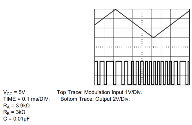
More info on how to use IC 555 for generating PWM
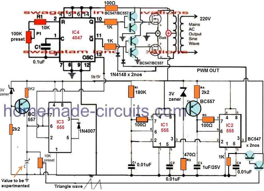
An RMS adjustment could be added to the above design by introducing a pot voltage divider network across pin5 and the triangle source input, as shown below, the design also includes buffer transistors for improving mosfet behavior
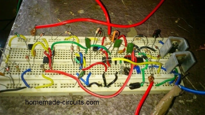
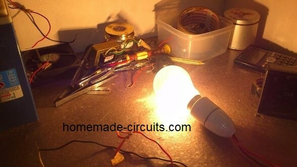
The above pure sine wave inverter design was successfully tested by Mr. Arun Dev, who is one of the avid readers of this blog and an intense electronic hobbyist. The following images sent by him prove his efforts for the same.
More Feedback
Inspiring response received from Mr. Arun regarding the above IC 4047 inverter results:
After completing this circuit, the result was amazing. I got full wattage by the 100 W bulb. Couldn't believe my eyes.
The only difference i had made in this design was replacing the 180 K in the second 555 with a 220 K pot to adjust the frequencies accurately.
This time the result was fruitful in all respects... On adjusting the pot, i could get a non disturbing non flickering full wattage glow in the bulb, also the 230/15 V transformer connected as the load gave a frequency in between 50 and 60 ( say 52 Hz ).
The pot was adjusted gently to get a high frequency ( say 2 Khz ) output from pin#3 of second ic 555. The CD4047 section better calibrated to get 52 Hz at the two output terminals....
Also I am facing a simple problem. I have used IRF3205 mosfets at the output stage. I forgot to connect the safety diodes across the drain terminals of each mosfets...
So when I had tried connecting an another load ( say table fan ) in parallel to the given load ( 100 W bulb ), the glow of the bulb also the speed of the fan was reduced a little and one of the MOSFET was blown due to the absence of the diode.
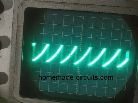
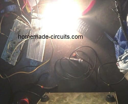
The above 4047 sine wave inverter circuit was also tried successfully by Mr. Daniel Adusie (biannz), who is a regular visitor of this blog, and a hardworking electronic enthusiast. Here are the images sent by him verifying the results:
Sawtooth Waveform Oscilloscope Output
Illuminating a 100 Watt Test Bulb
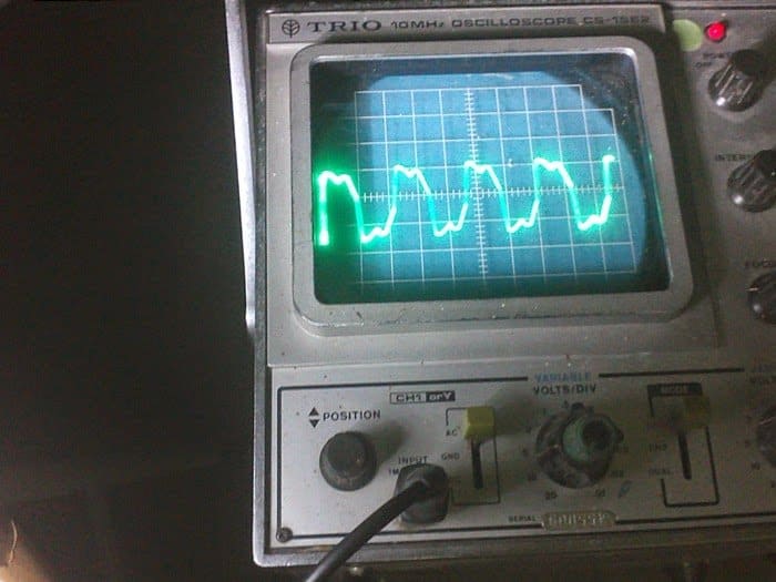
The following images show the modified waveforms at the output of the transformer as captured by Mr. Daniel Adusie after connecting a 0.22uF/400V capacitor and a suitable load.
The waveforms are somewhat trapezoidal and are far better than a square wave which clearly shows the impressive effects of the PWM processing created by the IC555 stages.
The waveforms could be probably even further smoothened by adding an inductor along with the capacitor.
Showing an near Sinewave Oscilloscope Trace after PWM Filtration
Interesting feedback received from Mr. Johnson Isaac who is one of the dedicated readers of this blog:
Good day
In your post, Pure Sine Wave Inverter using 4047, in the second I.c stage (ic.1) you used 100 ohms resistor in between pin 7 and 6.,
Is that correct? I use to think an astable multivibrator using 555 pin configuration should have the 100 ohms between pin 7 and 6. Also, the 180k variable between pin 8(+) and pin 7. Pls check the pin connection and correct me pls. Because it oscillate sometimes and it doesn't sometimes also. Thanks,
Isaac Johnson
Solving the Circuit Issue:
In my opinion, for a better response you can try connecting an additional 1k resistor across the 100 ohm outer end and pin6/2 of IC1
Johnson:
Thank you very much for your response. I actually constructed the inverter you gave in your blog and it worked.
Though I don't have an oscilloscope to observe the output waveform BUT I bet readers its a good one cos it operated a fluorescent tube lamp in which any modified or pwm inverter can't power on.
See the picture sir. But my challenge now is when I add load, the output flickers sometimes. But am happy its a sine wave.
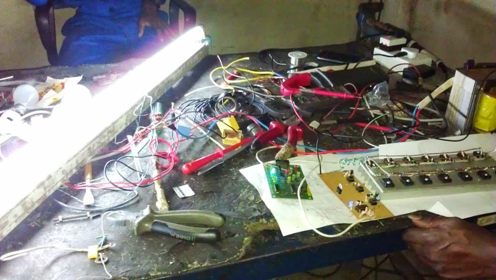
Video Test Waveform
Simplifying the above Concept
The above explained IC 4047 pure sine wave inverter can be actually simplified greatly by eliminating two IC 555 configurations from the design.
The basic idea is to produce a synchronized sine PWM output for chopping the MOSFET switching so that this SPWM waveform is replicated at the output of the transformer and is transformed into a pure sine waveform. The complete circuit diagram can be seen in the following diagram:
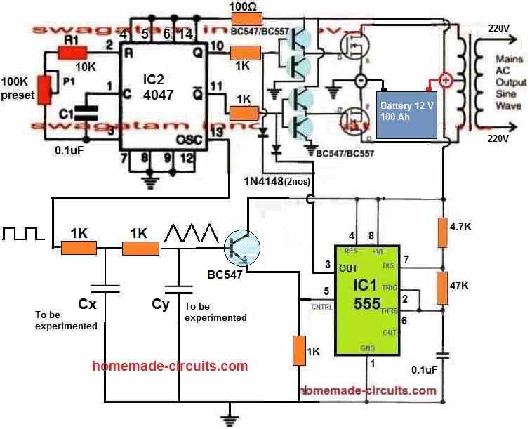
In this simplified design, we yet again exploit the pin#13 square wave output from the IC 4047 and convert it into triangle waves. This triangle wave is then used to modulate the PWM output of a IC 555 astable to create the required synchronized SPWM for chopping the MOSFET gates.
The capacitors Cx and Cy will need to be experimented a bit to create a proper triangle waves from the RC network output.
Remember, you will need an oscilloscope to check and confirm the various waveform discussed in the above diagram.
Another Simpler Looking Options
The following concept discuses a rather simpler method of modifying an ordinary square wave inverter using IC 4047 into a sine wave inverter through PWM technology. The idea was requested by Mr. Philip
Technical Specifications
I hope that i am not going to be a bother, but I need some advice with a PWM-controlled modified sine wave inverter I am designing so I want to seek your expert opinion.
This simple design is tentative, I haven't implemented it yet but I would like you to take a look at it and tell me what you think.
Also I want you to help answer some questions which I have not been able to find answers to.
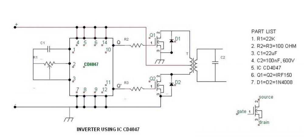
I have taken the liberty of attaching an image of a quasi-block diagram of my tentative design for your consideration.
Please help me out. In the diagram, the IC CD4047 in the inverter is responsible for generating square wave pulses at 50Hz which will be used to alternately switch on MOSFETS Q1 and Q2.
The PWM circuit will be based on IC NE555 and its output will be applied to the gate of Q3 so that Q3 will provide the PWM. Besides this, I have two questions.
First, can I use square waves for the PWM pulses? Second, what is the relationship between PWM frequency and supply frequency? What PWM frequency should I use for a 50Hz inverter output?
I hope that this design is feasible, I think it is feasible, but I want your expert opinion before I commit scarce resources to implement the design.
Looking forward to hearing from you sir!
Sincerely, Philip
Solving the Circuit Request
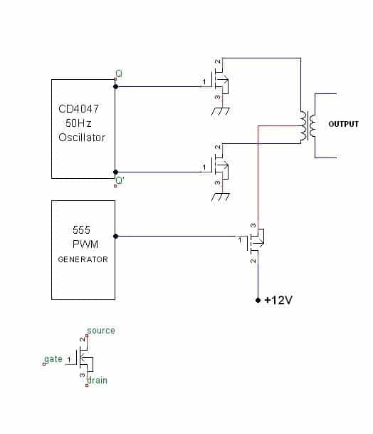
The configuration shown in the second figure above would work only if the center tap mosfet drain/source pins are swapped and N-channel mosfets are used for the 4047 inverter oscillator output, as shown below:
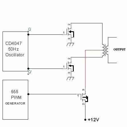
The PWM section should be built as I have explained in this article:
The PWM transforms the flat square waves into a modified square wave by chopping them into smaller calculated sections such that the overall RMS of the waveform becomes as close as possible to an actual sine counterpart, yet maintaining the peak level equal to the actual square wave input. The concept may be learned in details here:
However the above transformation does not help to eliminate the harmonics.
The PWM frequency will be always in the form of chopped square waves.
The PWM frequency is immaterial and may be of any high value, preferably in kHz.
How to Add Feedback Voltage Control to a 4047 IC Inverter
In this section we will discuss how to add an automatic feedback voltage control to a 4047 IC based inverter circuit.
If you don't want to read the whole explanation, you can watch the following video instead:
This type of feedback network is intended to ensure that the AC output voltage from the inverter never exceeds a predetermined safe value. For example, using this automatic feedback control, a 220 Volt inverter circuit output could be restricted to maximum 230V AC level, which may be safe for most 220 Volts appliances.
For a 120 Volt inverter system, this feedback network could be adjusted to restrict the output AC to a maximum of 115 Volts AC, which may be safe for most 110 Volt appliances.
How the Feedback Circuit Works
Now let's understand how the simple feedback network is designed to work, by referring to the following circuit diagram:
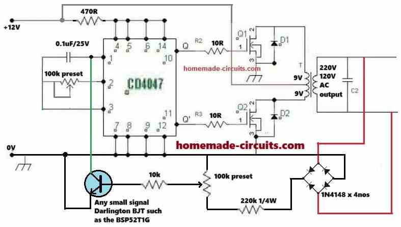
The mains AC voltage from the inverter transformer secondary is first converted to a DC voltage using a bridge rectifier.
This bridge rectifier is built using 4 numbers of 1N4148 diodes.
The DC 220 Volts output from the bridge rectifier is applied to an adjustable voltage divider network built using a 220 k resistor and a 100 k preset or trimpot.
The 100 k preset is carefully adjusted such that its central wiper terminal generates around 1.2 volts in response to an input AC voltage which is considered high, and needs to be restricted.
Let's say, the input AC needs to be restricted at around 270 Volts, then the 100 k preset may be adjusted so that its wiper terminal generates a proportional DC voltage level of 1.2 Volts.
We select a 1.2 Volt output because this is the equivalent DC level required to just switch ON the attached BJT device.
That means, whenever the inverter output AC voltage tries to exceed the 270 Volts mark, it causes the BJT to turn ON and become conductive.
When the BJT conducts, it starts grounding the CT pin of the IC 4047.
Since the RC network associated with the CT and the RT pinouts of the IC determines the output frequency and PWM, the grounding of the CT pin instantly causes the output PWM and frequency to nullify, which in turn causes the output AC voltage to dip.
When this happens, the feedback voltage to the BJT also drops proportionately until the BJT is turned off. In this situation the IC output PWM is restored back to its previous form, and if the output voltage continues to rise, it yet again activates the BJT via the feedback network, and this feedback on off cycle keeps repeating rapidly, ensuring that the output AC is not able to rise above the set threshold, which is 270 volts in our example.
This concludes our feedback control circuit explanation, now let's try to understand how this feedback circuit can be setup prior to integrating it with the inverter circuit.
How to Setup
The next diagram below shows the isolated feedback circuit, which can be set up by implementing the following steps, before interfacing it with your inverter circuit:
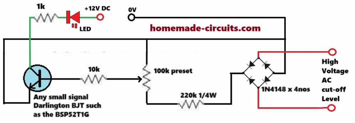
Initially keep the 100k preset's wiper arm fully towards the ground side of the DC supply.
Now, switch ON the 12 DC supply and then switch ON the AC supply to the bridge rectifier whose voltage level is around the desired high cut-off limit.
Next, slowly adjust the preset using a well insulated screw driver, until the LED just begins to illuminate.
To confirm the results, try varying the input AC voltage around the cut-off threshold and watch the LED turn on and off at the thresholds. Although the cut-off may not be too sharp, yet it will do the job of the intended output voltage control of the inverter quite well.
That's it! This simple procedure should be enough to complete the setting up of the feedback circuit.
After this, make sure to seal the preset adjustment with some super glue.
So, this concludes our explanation on a feedback circuit for the 4047 inverter.
Pseudo-sinusoidal IC 4047 Inverter Circuit
From a continuous source, battery, or vehicle alternator, it is possible to produce a 50 Hz voltage/pseudo-sinusoidal waveform, using this simple IC 4047 inverter circuit. The design is capable of operating many low-power devices that require a voltage of 220 V AC, typically supplied by the AC mains grid distribution network. The power of this module depends largely on the chosen transformer and, above all, on the continuous source's ability to supply the circuit without failure.
Working Principle of the circuit
Being able to power a device on the 220 V AC network when no mains AC power is available can be very convenient. We particularly think of campers, caravanners, fishermen, and motorists.
Although this simple setup does not provide a 100% clean sinusoidal wave, it can still satisfy many undemanding devices such as incandescent or fluorescent lighting, soldering irons, small motors, etc.
The power can reach up to 250 VA if the continuous source is strong enough and an adequate toroidal power transformer is chosen.
The power transistors are rated for 30 A, provided that a substantial heatsink is used.
We even suggest adding a small fan directly connected to the 220V output, which will prevent it from operating without a load.
Analysis of the Circuit Diagram
To obtain an alternating voltage from a DC source, the simplest solution is to use an inverted transformer: the low-voltage secondary winding has a center tap.
It is then sufficient to alternately supply power to the two windings to produce a symmetrical, but non-sinusoidal, variable voltage on the primary side if the low-voltage secondary winding is driven by a rectangular signal with steep edges.
Two complementary and opposite signals are required, and the CMOS integrated circuit with the reference 4047 is used to generate them, capable of either building an astable or monostable flip-flop.
The proposed diagram is shown in the figure below.
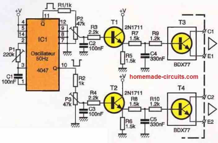
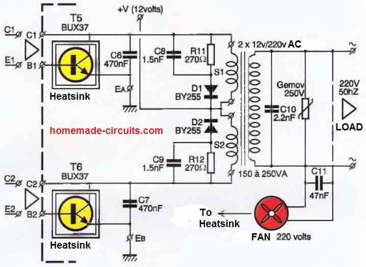
Of course, we will operate our circuit as an astable generator, ensuring a precise frequency of 50 Hz. This task is entrusted to components C1 and P1. Some pins of the IC1 circuit are connected to the ground or the positive supply, depending on our needs.
For more information, you will find an explanation in the appendix about the multiple possibilities of this practical little integrated circuit.
The symmetrical square voltages available at pins Q and Qdash (corresponding to terminals 10 and 11 of the circuit) are routed through resistors R1 and R2 to an adjustable element. Its role is to balance the amplitude of the two signals and facilitate the adjustment of the control module.
Note that the duty cycle will be exactly 50% by design. The sliders of elements P2 and P3 control the base of a 2N1711 transistor, which is responsible for driving the downstream power semiconductors.
Components R7, R9, C4, as well as R8, R16, and C5, form a coarse filter capable of smoothing out the signal angles to some extent.
This will allow us to create a "pseudo-sinusoidal" signal that will control the intermediate transistors T3 and T4 mounted on the small control board.
The BDX 77 models are rated for an emitter-collector voltage of 80V and a maximum peak current of 8A. They are delivered in a TO-220 package and will benefit from a heatsink.
The secondary windings of the transformer do have a common point connected to the positive pole of the power supply.
The other end of the coils will receive the ground through the power transistors T5 and T6, a model not much larger than the famous 2N3055 but with a maximum peak current of around 30A in this case.
It is the NPN bipolar model with the reference BUX 39.
Diodes D1 and D2 absorb the unavoidable breakdown current produced at each interruption of the inductive element, which is the transformer.
The primary of the transformer, a toroidal model in this case, delivers a 50 Hz AC voltage.
The component labeled Gemov (or varistor) is placed between the output pins to clamp excessive voltage surges that may occur.
Two wires can also be tapped from the output to operate a fan directly powered by 220V, which will provide airflow to cool the transistor-heatsink assembly.
It is important to ensure that the voltage of the continuous source does not drop too much or be completely depleted in the case of a lead-acid battery.
It goes without saying that the input DC current can reach considerable values if, for example, a power of 200VA is desired. It would be prudent to include a robust series fuse, similar to those found in a household installation.
Construction
The creation of two printed circuit boards is necessary: the first one, shown in the figure below, is designed for the components described in the control module.
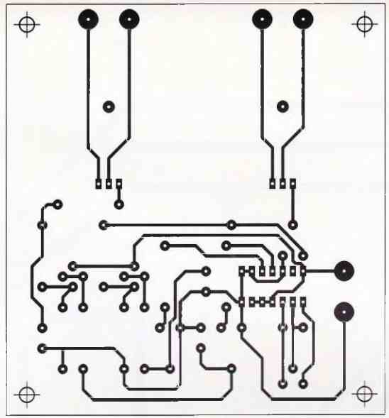
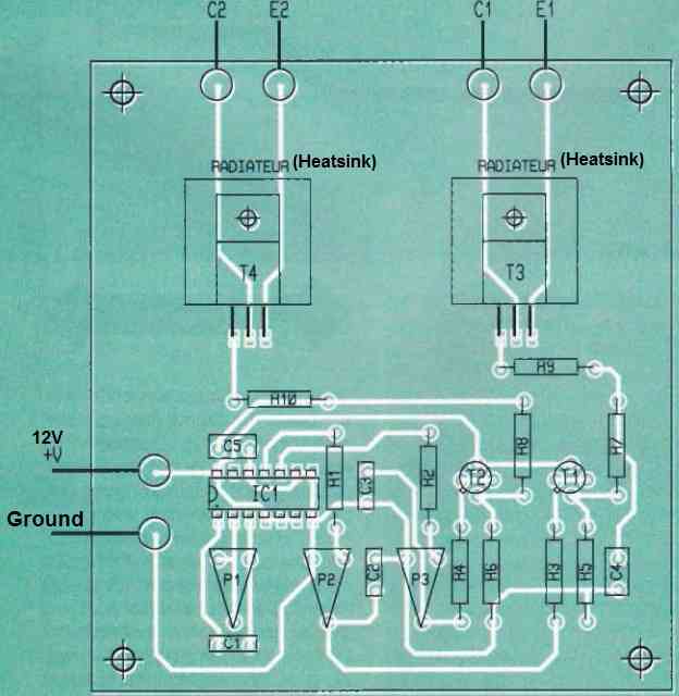
The layout is not very dense, but it is still recommended to use pre-sensitized copper-clad boards for reproduction.
After etching and rinsing, various drillings are carried out. Care must be taken to carefully mount transistors T3 and T4 on a small heatsink, which is directly attached to the epoxy board.
From this board, six wires will go to the significantly larger power module, and the track layout at a 1:1 scale can be found in the figure below.
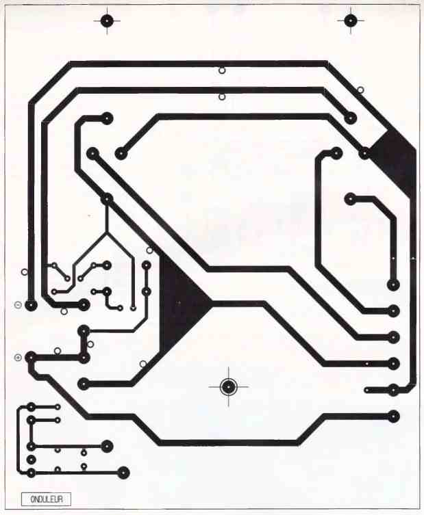
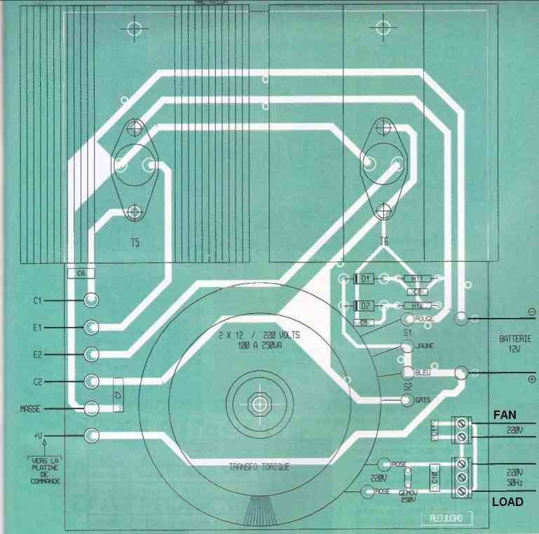
It should be noted that certain tracks on this simple IC 4047 inverter circuit board will carry high currents and require special treatment. We recommend soldering bare copper lengths, with a section of approximately 1.5 mm2, directly onto these tracks.
For example, electrician's copper wire with the insulation removed can be used. Care should also be taken to ensure all connections between the two boards, and in particular, to avoid reversing the wires.
The transformer has six wires, with the two thinnest wires corresponding to the primary, and therefore our 220V output.
It is important to properly identify the other windings before soldering them permanently. This assembly can be housed in a sturdy, adequately ventilated metal enclosure.
How to Setup
We leave it to you to complete this final step for this simple IC 4047 inverter circuit. After a thorough check, the frequency can be adjusted to 50 Hz under no-load conditions using the adjustable preset P1, if you have an oscilloscope or frequency meter.
Otherwise, simply set this element to the midpoint position. The other two adjustable components are set to obtain a symmetrical signal in amplitude.
Initial tests can be performed using a simple socket where different power lamps can be connected. For resistive or slightly inductive loads, there should be no serious issues.
Proceed with caution when testing devices that typically require a true sinusoidal voltage.

you can use polar cap, since one of the leads of the capacitor can be seen connected with ground, so it’s fine…
Sir can I connect more power capacitors to the inverter dc supply in parallel? Is it recommended or they will impact the outcome.
You can add, there’s no problem with it.
if I want to produced output power of 500watts,50Hz
which components do I change and at what ratings?
also what would be the ratings of transformer to be used?
what voltage do you intend to use for the battery?
Dear sir i purchase local inverter kit for my inverter how can set drive preset please tell me
Dheeraj, sorry I won't be able to advise without seeing, I think you should contact the dealer for the details.
I'm young king sir pls there is question I want to ask like u said that tip35 can accept minimum of 25 amps, now if I want to use more number of tip35 how do I determine my trans4mer amperage and battery amperage.I'm waiting for or responds
Primary Transformer amperage should be equal to the result achieved by dividing the required output wattage by the battery voltage
I have a 30V battery, so can I use a 15-0-15 trafo for this circuit ?
Do you have a PCB for this circuit
Hi sir, I have a 30V battery, I want to know if I can use a 15-0-15 trafo for this circuit?
P/S: Do you have a PCB for this circuit?
Hi Colby, you can use a 30V supply but in that case make sure to replace the 100 ohm top resistor with a 7812 IC so that the ICs are supplied with 12V and not 30V…sorry I do not have a PCB design for this….anyway you must first try it on a breadboard before going for a PCB…
hello sir thanxx for sharing your knowledge …..i have made your simple circuit i got 220 volt ac o/p but its not suitable for my 100watt tv ,or Watt led bulb i think that device operate only pure sine wave .please is it possible to run 100 watt tv by using this circuit ?? ..i want to make 300watt pure sine wavw inverter.
Heelo Ravindra, the design explained in the above article can be used for operating all kinds of equipment, even your 100 watt TV etc. It is almost a pure sinewave inverter circuit….
By the way do you guys realize the current draw from battery there is no load added, also the current draw is higher when it's running for the first minute then it's current draw goes down along with the output voltage.
I haven't gotten the time to build the 4047 board alone as yet but I'll just separate the one I have from the others since I spilt the build in 3 and test it
hi sir i have used ic 4047 and mosfets irf150 .first time the circuit runs properly but whenever we apply load after some time of first test then the ic is not working properly.i have used 12V battery of 7 amph. ic gives only oone pulse. kindly suggest me the solution > thanaks
Hi, the IC has no direct connection with the load so it should not get affected by the load.
use an IC socket for the IC and try other ICs to see whether the specific IC is faulty or it's happening with other ICs also….
Hi Swagatam
It's great to see someone has built this inverter succesfully.
I would like to know why you use current controlled generator for the sawtooth and PWM sections instead of a normal 555 oscillator
Thanks Robin,
the current controlled stage ensures that the triangle waves do not get disturbed or change their specifications in response to a varying supply voltage, so this is specific reason for including the BC557 stage
I tried this circuit in the past I normally have frequency issues then.
Now I'm not getting the frequency to be adjusted, I have a video you can watch.
https://youtu.be/FHiWJV4EAaQ
The voltage is also low, in this test my battery is at 12.2v
the frequency is determined by the R/C components of the 4047 IC, you can try building the 4047 section separately and set the frequency first.
if still it does not work then may be your IC could be faulty.
Hi!How can we get the output frequency of 20-40khz for this inverter
Hello Hari, you can do it either by decreasing the associated resistor value or the capacitor value…or both together, for getting the desired level of high frequency output…increasing the values will decrease the frequency
hello Mr.Swagatam. We are trying to make a project for wireless transfer of power using induction principle. For that we require high frequency inverter of nearly 20-50khz. Can u suggest how to trigger those MOSFETs. Thank you
ok.According to you, which is better, using two battery 12volts 45ah in parallel with a transformer 6volts or two batteries 12volts in series with a transformer 12 volts? or it's the same performance?Thanks
the second option is recommended, but the trafo could be preferably 18V not 12V
Thank you very much, I finished to make it work,it's good to seen it , but is it normal that the transformer emits a sound? And how to integrate automatic voltage correction according to loads, I have already seen your old post for this but I have trouble for integrating it, can you send me a diagram to integrate it or explain how do ? Thank very much
thank you…adjust the PWM freq to reduce the noise, a 150 or 200Hz for the PWM will be enough and help to keep the noise low.
for the automatic correction , you can refer to the following design
https://www.homemade-circuits.com/2014/01/automatic-output-voltage-regulator.html
connect the BC547 collector directly with pin#5 of the PWM IC 555…the diodes on the BC547 collector can be ignored and removed
Thank you and have you an circuit to automatically adjust the output voltage because it drops when I increase the load or how to do it?
If the voltage is dropping below the normal 220V level then no circuit can prevent that, because it may be happening due to an overload where the load current or wattage could be exceeding the optimal specified battery/transformer wattage.
Hi, thanks for your post, I built this converter but I have some difficulty. If I use a 6V-0-6V transformer as you indicated with batery 12v , the mosfets will heat up to one minute and the output voltage will be approximately 350 volts without diodes and 400volts with two diodes connected.Why??? I get 50hz on pin 10 and 11 and 100hz at pin 13 of the CD4047.if I use a 15V-0-15V transformer I get 205volts at the output without the diodes and 220 volts with two diodes connected.and no heating at Mosfet, is it really necessary to use a transformer 6V-0-6V.help me,where is problem? thank you very very much
Hi, connecting the PWM should reduce the RMS voltage, it should not increase the RMS, I think you might have connected the diode in the opposite direction.
I recommend the second diagram from top, which is more suitable for the diode PWM integration.
please check the diagram again.
6-0-6 is recommended so that the 350 voltage could be brought down to 220V after the diode (PWM) integration.
Thank you, another problem please, I used two IRF3205 for a test, I get 220 V after adjusting the RMS 10k, the problem is the mosfet temperature is too high even if no load, it works about 1 or two minutes and one of the mosfet is damage. What can I do to solve this ?
remove PWM feed from the mosfets and check again, if the mosfets stop heating then the reason could be high frequency from PWM, reduce it to 200Hz or 150Hz and recheck.
If without PWM it's still heating up then there could some other hidden fault in your design
No additional resistor needed to the Gate for the all mosfets??thank you
it won't required, just keep the connections as short as possible.
Hi, I built this converter, I get 100hz on pin 5 and 2 kHz high frequency on pin 2 of the IC as you indicate. My problem is that I get 50hz on pin 10 and 11 of CD4047 when I remove the 10k resistor between pin 9 of the CD4047 and the positive (+). but it generates a high and different frequency at pin 10 and 11 of CD4047 when I connect this resistor. why? can I remove definitely this resistor or change for another value?what is the impact on circuit behavior?thank for your post
Hi, please try the second circuit, the pin9 concept is just a recommendation, it's not a confirmed design, so it's better to go for the first or the second designs which are tested and confirmed ones.
thank you for your reply , if I choose the second circuit, how connect the two diod for a multipl mosfet to increasing more wattage?
the diode and the BJT section will not change, multiple mosfets can be included by simply connecting their G,D,S terminals in parallel with each other.
Sir,
I searched the current rating of IC4047 and could not find it . It is required to decide the load capacity . So please help me to know the current rating of IC4047.
Thank you sir
Alkok, the current consumption of 4047 is 5mA to 10mA….load capacity???
Load capacity of an inverter is determined by the trafo, battery AH and the mosfets….
Hi, pls is there any modifications done on the diagram? I will love to have it. Also, pls what is the power rating (wattage) of the inverter? Thanks
I've completed the oscillator,but little problem I encounter is that when I tested it with two energy saving bulb it works but when I try to include fan to it does not work.
With sg3524 oscillator that I built it works perfectly. Please any idea of little correction I can make to the circuit
THe RMS value must be adjusted to make sure it is upto 230V, if the peak is 330V.
there's no difference between the oscillation characteristic of 4047 and 3524, so IC is not the problem….the RMS needs to adjusted to the correct level for operating the fan.
Hello sir
The oscilator works with one energy saving bulb.but if I tried to increase the load. Eg TV or fan the inverter will not work.when I reduise the load the the bulb alone it will on.please what adjustment can I do to the oascilator
Hello yusuph, the output power will depend on the transformer wattage and the battery AH, so you will have to increase the ratings of these two parameters in order to be able to operate more loads at the output
2.7V or 3V
pls need quick response.pls what is d name of the component you marked 1mA which is connected to the collector of bc557 and connected through 100ohm resistor to pin 7 of the last 555.tnk waiting for ur response.
that's an arrow symbol not a components….just ignore it.
thanks alot.wil gv feedbk when am done making and that should b after my exams.thankx
thanks for the quick response.wl make this after my exams and wl tell you how it goes.hope i can rate it upto 5kwatt and how can the voltage b made stable at 220v even with increasing load.thanks again
voltage correction can be done by using this circuit:
https://www.homemade-circuits.com/2014/01/automatic-output-voltage-regulator.html
i lov dis inverter .have made some of ur inverters which worked pretty well.bt i want to make dis cos it sine wave n uv made it so simple.the problem am havin is how to add more power that is,adding more fets in parallel.u said d pwm integration should b connettd to pin 9 of d ic cd4047 as shown in d last diagram.bt other diagrams above shows pwm integration at the base of the bc547 transistors.am confused is it dat if i want more power i should use the last diagram.pls xplain to me .waiting for ur reply.thanks
I would recommend the second schematic from top, which uses BJT buffer stage.
pin9 was just a suggestion but I am not sure about its outcome, so better to go with the earlier diagram using diodes and BJT buffers.
for more power you will need a higher rated transformer and battery in terms of voltage, and lastly appropriately rated mosfets, the IC design is not relevant to the power outputs specs
ok will do, just have so much things working on.I know your busy I am not sure how long it would take you but could you make a pcb layout for this if possible.
sorry, designing PCB would not be possible at the moment,
I was trying to increase the power of this inverter by adding 4 irfz44n to each side but when I do that they keep blowing up as I apply power, before applying power I ensure to check for short circuit across the legs and there is none and only 1 side of the fets keep blowing up, I used 10ohm resistors fr gate resistance but on 1 side I used some 3 watt 10ohms and on the other side I used some 1/4w 10ohm resistors and the side that keeps blowing all the fets is the side with a 1/4w resistors I am wondering if thats the problem or is it that I should use higher gate resistor, probably 100 ohms.
what happens with single mosfets, does it work normally with single mosfets??….if you are using breadboard then that's not the right approach…a PCB is strictly required.
higher gate resistance will make it even worse…try connecting 1K resistors across all the mosfet gate/source.
sure surprisingly I am now building circuits but I have a problem when I try to make inverters with large power since I need to use large cables I don't know how to connect those large wires to the fets I use and I cant find any type of connector I could connect to the fet the solder big wires to it, is there anthing you can recommend
how large are they?
you can clamp them with nuts and bolts on the PCB, or you can fix by soldering using 100 watt solder iron
or simply think about increasing the voltage spec…the current requirement will decrease proportionately
I am in Jamaica we dont do electronics here at all we import all form of our electronics, we only repair here, I love electronics and I try to build every circuit that I see you upload just for fun, at times I end up building them and using them also.
OK thanks, keep up the good work
One other thing, do I add diodes accross each fet on both sides or across 1 Fet on each side
single diodes across center tap and the outer taps of the trafo will be enough.
cathode will be towards center tap
yes sorry I didnt read your previous message properly either.
So I built this today on a larger scale and attacked a bigger transformer rewonded microwave transformer not sure of the wattage, but I only attacked 2 Irfz44n for testing the voltage was at 124v before load, when I added the fan and turned it on it went to 113v.
Pcb boards online seem so very expensive there is no local manufacturer in my country that does Pcb, could you reccommend me to an online store that does it at a reasonable cost.
Also did you do any Pcb for this design that would be handy.
I am sorry, I do not know about any online PCB manufacturer who can provide at a cheaper rate, by the way in which country are you in?
I haven't been able to yet design the PCB for the above due to lack of time.
Ok you told me how to connect the diode to the battery cathode to positve and then leave the anode open for charging input, but what about how to turn the diode at the center tap of the transformer how do I turn that one.
you mean the polarity?
it should be anode to batt, and cathode to center tap.
question, about the reverse polarity seems as if thats for if the output of the transformer was the be shorted how would I connect the diode anode to battery positive and cathode to transformers center tap?
What about reverse polarity protection on the battery side
the center tap diode is for protecting the inverter circuit from a reverse batt polarity.
for protecting the battery from reverse charging current you can connect another diode to the batt positive..cathode to positive and anode open for charging input
OK then, since it's working as is im remove it from the proto type board and Solder it up, so I will need additives
1) a circuit to cut off battery power probably at 10.5v and also cut off at 14.5v (just guessing a range)
2)reverse polarity feature for the battery side or for both side,
3) normally people talk about feed back what is that refering to really?
4)low and high vtage alarm.
Any other thing you can think of, to do this I guess I would redraw the schematic, which software do you use to draw
1) you can use the second circuit from the following link:
https://www.homemade-circuits.com/2011/12/how-to-make-simple-low-battery-voltage.html
2) reverse polarity can be implemented by ading a diode with the transformer center tap
3) for feedback control you can try the following circuit
https://www.homemade-circuits.com/2014/01/automatic-output-voltage-regulator.html
if possible I'll try to update the new diagram…
ok thanks, using the TL 072 it can generate a pure sinewave? if so I would be able to add it to pin 9 of 4047 to make a pure sinewave then.
a TL072 bubba oscillator will generate sinewave but it will have no effect on pin9 of the IC…it will be treated like a square wave only.
Hi Swagatam Majumdar
i really want to thank you for your assistance all this while. i have build a 2kva inverter of the above circuit and it work when tested. please i want to ask can this inverter withstand load? also can i incoporate feedback in other to withstand load if a feedback can be incoporate were can it be place in the circiut thanks and
Best Regard
Thanks Faith,
load handling capacity will depend on the trafo wattage and battery AH level…
you can use the following idea:
https://www.homemade-circuits.com/2014/01/automatic-output-voltage-regulator.html
you can connect the diode ends with the bases of the BJTs just like the PWM diodes configuration
I just noticed something rite where I have the problem at ic2 with the 100ohm resistor on pin 7, is that a diode connecting it to the collector of the transistor? If so I dont have a diode there and that would be the problem.
that is just an arrow symbol, indicating a 1mA current through that path….it's not a diode
Ok will do.
Also since its working the way it is now I am wondering if it can stay that way, I have a project coming up and I need 2 inverters a pure sine and a modifed sine I plan to use this as the modified sine thats why I didnt want to take out the triangle wave portion.
Could you help me to achieve a pure sinewave also?
The last diagram in the following article is possibly a pure sine wave inverter circuit:
https://www.homemade-circuits.com/2012/05/make-this-1kva-1000-watts-pure-sine.html
OK thanks,I fixed the issue which was at the ic1, middle ic…. The resistor at pin 7 was shorted by mistake I connected it correctly and I got a better wave, also where you have a 180k resistor I have a 250k pot for me to get 50hz I have to adjust that pot clockwise all the way and then add (3) 0.22uf caps in parrallel across pin 1 and 3 of the 4047 and adjust the pot on the 4047 to get 50hz at 125v…
But then I realized the resistor at ic1 kept smoking so I thought because of the short I damaged the ic, so I changed the 555 and also changed the resistor again but the samething keeps happening, so what I did was to add a 1k resistor in place of the 100ohm it's a 1watt and it works fine now, doesnt really get hot, but I realize the reason why the 100ohm got hot is because of the way i turned to 250k pot all the way down and what I realized is that across the pot I am getting 12.4v in which if I turn it back up where it doesn't get hot I have no voltage across it, so I am wondering if I should really leave it like that.
The voltage I have it set to now is 124v and frequency at 56hz which I need 50hz but if I adjust it to 50hz the voltage goes all the way up to 134v and That may cause problem when testing electronic loads even though the voltage will drop when loaded.
Link to wave form
https://www.dropbox.com/sh/vz9c54gvxy0evni/AACVGaRo_Pn9URcjxRAt6exVa?dl=0
try removing the triangle wave generator entirely because anyway the perfect sine simulation is not essential….and now configure the pot across the supply using a 1K pot….as shown in the following diagram.
1.bp.blogspot.com/-jONLYQ8Ehro/UkD_gzAjA-I/AAAAAAAAFSk/nt6vxMDF9RU/s1600/ELC+circuit.png
use a 1K pot instead of the shown 10k..and please ignore the other irrelevant things in the design
adjust the this 1K pot to set the PWM and the RMS of the output, I hope this will be easier.
I built this just now I am having some problems I am wondering if one of the ic is giving an issue, or I am probably just using the wrong pot and capacitor on the 4047.
1) main problem is that most times I applied DC power I don't get any output from the transformer if I don't turn the pot connected to the 4047 ic it comes on when the frequency is high, at times I will change around the capacitors and it come on at a lower frequency I am using 0.22uf sometimes I try 1 or parrallel 2 or even 3, I even try 0.1uf and also 0.01 one of the mixture alone with the 10k pot gave me 50hz at once but when ever I turn off the DC power and turn it back on the circuit won't come on until I adjust the pot to a higher frequency.
2) voltage is good but I am actually getting a square wave output instead of the modified wave seen in the examples.
3) link to pics
https://www.dropbox.com/sh/m8td2zeavt2m5q5/AAA8d8VryZDM72pkYrhOZvcMa?dl=0
the issue could be with the IC specs, you can check the datasheet of the IC to see the optimal min/max values for the Rt, Ct
if you are getting square waves then it means the 555 stage is not working…check the 555 stage separately and make sure pin3 produces varying pulse widths in response to the lower pot adjustments….
check the pin3 of IC2
ok so each additional Fet would need a 10k resistor added to its gate, and I wouldnt need to add any more stages of those transistors controlling the fets.
yes 10 ohms with each gate, (not 10k)….no additional BJT buffers would be required for the parallel fets
Wouldnt it be more of a pure sinewave connecting a coil across the output of the transformer, what value coild could be used if so? also is the modified versin of the schematic a better version using the transistors before the fets? if so How would I add FEts in parallel?
LC can be used in conjunction with PWM for improving the results but without PWM it could be much inefficient.
the bJT stage ensures better isolation from the PWM and a better discharge of the fet gate capacitance improving its performance.
you can still add fets in parallel with the BJT by simply using individual gate resistors with each of the fets
hi mr swagatam,how are you.
congratulation for new site design,
i want to share with you a pure sinewave inverter using pic16f72 microcontroller
give your mail and i will send you files and you can share it here with all people.
best regards
Thank you very much Hisham, Please send it to
admin@162.240.8.81
but please do not publish it anywhere else:)
Good Day Sir, I'm Alfie. what is 1mA between BC557 to 100 ohm resistor?
it's the amount of current that is expected to flow through this connection
yes i will use 2kva transformer and a battery of 12v/200AH,though i did not test it with that i tested it with 9v battery and with 1.5tranf rated 500mA
can i use this this circuit to build up to 2kva, because the one i build i use 7 mosfet in parallel
increasing only mosfets will not do, the transformer and the battery will also need to be upgraded…for 2kV the battery will need to be minimum 500AH rated.
the one i build is the third one and the output of the 3 ic is fed to pin 9 of pin of the 4047 ic not bufer please i can see the one you are referring to
I am referring to the following design:
1.bp.blogspot.com/-8KGsjPyAqbI/VmPJvg8dENI/AAAAAAAAMC4/yJE2FXkBL_E/s1600/4047%2Brms%2Badjust.png