Schottky barrier diodes are semiconductor diodes designed with minimal forward voltage and fast switching speeds which may be as low as 10 ns. These are manufactured in current ranges of 500 mA to 5 amps and up to 40 V. Due to these features they become specifically suitable in low voltage, high frequency applications such as in SMPS, and also as efficient freewheeling diodes.
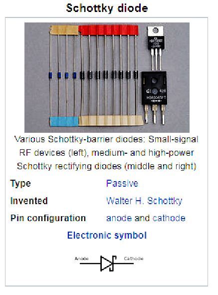
The symbol of the device is shown in the following image:
Internal Construction
Schottky diodes are constructed differently compared to the traditional p-n junction diodes. Instead of a p-n junction they are built using a metal semiconductor junction as shown below.
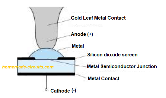
The semiconductor section is mostly built using n-type silicon, and also with a bunch different materials such as platinum, tungsten, molybdenum, chrome etc. The diode may have different set of characteristics depending on which material is used, enabling them to have enhanced switching speed, lower forward voltage drop etc.
How it Works
In Schottky diodes electrons become the majority carrier in the semiconductor material, while in the metal exhibits extremely small minority carriers (holes). When the two materials are linked, the electrons present in the silicon semiconductor start flowing rapidly towards the connected metal, resulting in a massive transfer of majority carriers. Owing to their increased kinetic energy than the metal, they are in general called "hot carriers".
The the normal p-n junction diodes the minority carriers are injected across a different adjacent polarities. Whereas in Schottky diodes electrons are injected across regions with identical polarity.
The massive influx of electrons towards the metal causes heavy loss of carriers for the silicon material at the area close to the junction surface, which resembles the depletion region of p-n junction of other diodes. The additional carriers in the metal creates a "negative wall" in the metal between the metal and the semiconductor which blocks further entry of current. Meaning the negatively charged electrons at the silicon semiconductor inside Schottky diodes facilitates a carrier free region along with a negative wall at the metal surface.
Referring to the figure shown below, applying forward bias current in the first quadrant causes a reduction in the energy of the negative barrier due to the positive attraction from the electrons in this area. This leads to the return flow of electrons in huge amounts across the boundary. The magnitude of these electrons depends on the magnitude of the potential applied for the biasing.
Difference between Normal diodes and Schottky diodes
Compared to normal p-n junction diodes the barrier junction in Schottky diodes is lower, both in forward and reverse bias regions.
This allows the Schottky diodes to have much improved current conduction for the same level of bias potential, across both forward and reverse bias regions. This appears to be a good feature in the forward bias region, although bad for the reverse bias region.
The definition of general characteristics of a semiconductor diode for the forward- and reverse-bias regions is represented by the equation:
ID = IS ( ekVd/Tk -1)
where Is = reverse saturation current
k = 11,600/ η with η = 1 for Germanium material and η = 2 for Silicon material
The same equation describes the exponential rise in current in Schottky diodes in the following figure, however the factor η is determined by the type of construction of the diode.
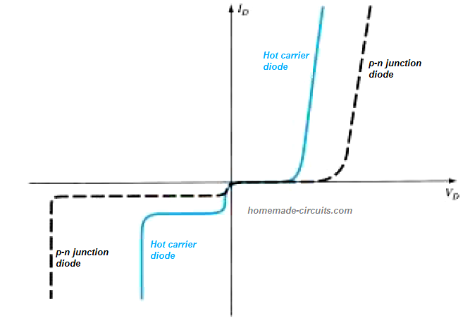
In the reverse-bias region, the current Is is mainly due to those metal electrons travelling into the semiconductor material.
Temperature Characteristics
For Schottky diodes, one of the primary aspects that has been continuously researched is how to minimize its substantial leakage currents at high temperatures over 100°C.
This has led to the production of better and improved devices that can work efficiently even at extreme temperatures between - 65 to +150°C.
In typical room temperatures this leakage can be in the range of microamperes for low power Schottky diodes, and in the range of milliamperes for the high power devices.
However, these figures are bigger when compared with normal p-n diodes at the same power specifications. Also, the PIV rating for a Schottky diodes can be much less than our traditional diodes.
For example, normally a 50 amp device may have a PIV rating of 50 V, whereas this may be up to 150 V for a normal 50 amp diode. That said, recent advancements have enabled Schottky diodes with PIV ratings over 100 V at the similar amperage values.
It becomes quite clear from the above graphical representation that Schottky diodes are attributed with an almost ideal set of characteristics, even better than a crystal diode (point contact diode). The forward drop of a point contact diode is typically lower than a normal p-n junction diodes.
The VT or the forward voltage drop of the Schottky diode to a great extent is determined by the metal inside. There happens to be trade-off between the effect of temperature and the VT level. If one of these parameters increases the other also increases degrading the efficiency level of the device. Furthermore, the VT also depends on the current range, lower allowable values ensure lower values of VT. The VT forward drop can be essentially down to zero for a given low level units, in an approximate evaluation. For middle and higher current ranges, the forward drop values could be around 0.2 V, and this appears to be a fine representative value.
At the moment the maximum tolerable current range Schottky diode available is around 75 amps, although up to 100 amps may also be on the horizon soon.
Schottky diode Application
The main application area of Schottky diodes is in switching power supplies or SMPS, which are intended to work with frequencies over 20 kHz.
Typically, a 50 amp Schottky diode at room temperature may be rated with a forward voltage of 0.6 V, and a 10 ns recovery time, specifically designed for an SMPS application. On the other hand an ordinary p-n junction diode may exhibit a forward drop of 1.1 V and recovery tome of around 30 to 50 ns, at the same current spec.
You may find the above forward voltage difference to be quite small, however if we look at the the power dissipation level between the two: P(hot carrier) = 0.6 x 50 = 30 watts, and P(p-n) = 1.1 x 50 = 55 watts, which is quite a measurable difference, that can harm the efficiency of the SMPS critically.
Although, in the reverse bias region the dissipation in a Schottky diode may be slightly higher, still the net forward and reverse bias dissipation will be much better than a p-n junction diode.
Reverse Recovery Time
In ordinary p-n semiconductor diode, the reverse recovery time (trr) is high on account of the injected minority carriers.
In Schottky Diodes due to extremely low minority carriers, the reverse recovery time is substantially low. This is why Schottky Diodes are able to work so effectively even at frequencies of 20 GHz, which require the devices to switch at an extremely fast speed.
For higher frequencies than this, a point-contact diode or a crystal diode is still employed, due to their very tiny junction area or point junction area.
Schottky Diodes Equivalent Circuit
The next figure depicts the equivalent circuit of a Schottky Diode with typical values. The adjoining symbol is the standard symbol of the device.
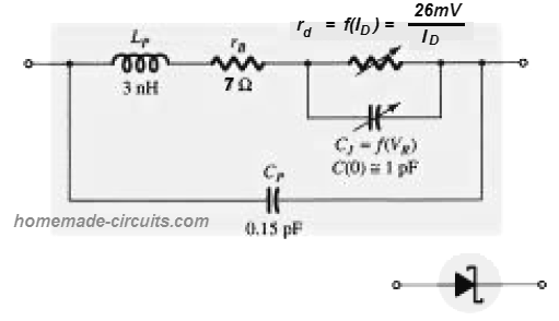
The inductance Lp and the capacitance Cp are the values specified in the package itself, rB constitutes the series resistance made up of the contact resistance and the bulk resistance.
The values for the resistance rd and capacitance Cj are as per the calculations discussed in the previous paragraphs.
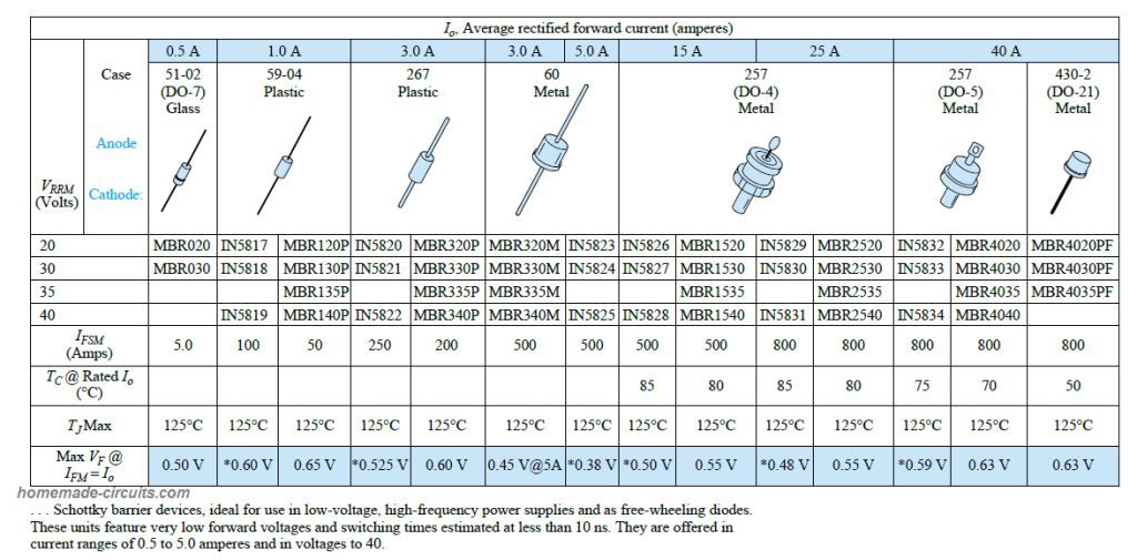
Schottky diode Specification Chart
The chart below provides us a list of hot-carrier rectifiers manufactured by Motorola Semiconductor Products along with their specifications and pinout details.
Applications of Schottky Diode
- Applications for the Schottky diode are numerous. It may, of course, be used as a general-purpose rectifier. However, because to its quick switching times and high-frequency capabilities, it is very advantageous for RF applications.
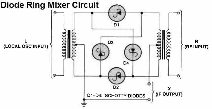
- Schottky diodes are thus virtually always used in high-performance diode ring mixers (shown in Figure below) in order to meet their performance criteria.
- They are also excellent RF detectors since they can pick up signals that a conventional PN junction would not because of their low capacitance and forward voltage loss.
- The Schottky diode has a high current density and a low forward voltage drop, as discussed previously.
- Because of this, Schottky diodes are usually applied in power supplies. These diodes reduce power loss, improving the power supply's efficiency.
- Additionally, because of the increased efficiency, lower heat needs to be dissipated, which may allow designers to use smaller heatsinks in their designs.
- Logic circuits incorporate the Schottky diode. The 74LS (low-power Schottky) and 74S (Schottky) series of logic circuits employ Schottky diodes as a key component, although being less popular nowadays.
- In order to serve as a clamp, the Schottky is inserted between the driver transistor's collector and base (see Figure beow).
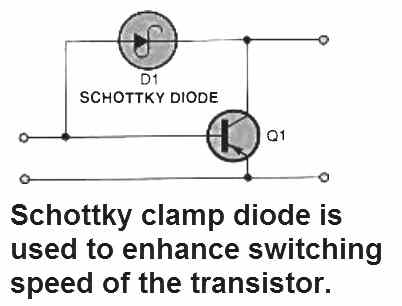
- The base-collector junction of the diode is forward biased when the transistor is turned hard on to generate a low or logic "0" output. The Schottky diode absorbs the majority of the current while it is functioning, which significantly reduces the transistor's turn-off time and speeds up the circuit.
- In addition, the Schottky diode serves as an essential component in a variety of other devices, such as metal-semiconductor field-effect transistors and photodiodes (MESFETs). This diode is not only widely used in several applications by itself, but it also serves as a critical component inside a variety of other devices.
Many thanks, very helpful. Pete
I am trying to find a circuit, using Schotsky Diodes , which will give protection to two 8.4v in parallel against back surge. ( For use in my model boats) Can you help, please?
Can you please specify what those 8.4 v devices are?
Sorry about that, I sail radio controlled model boats, most of which are powered by 8.4 volt NiHM batteries.. I would like to extend running times by using two batteries in parallel, but I am told that without some protection, there is a possibility of one discharging into the other and causing heat. There used to be on the market, a small circuit, called Action P103 Power Board, (no longer available) which used a Schotsky Diode mounted on a heatsink. The pos and neg of each battery was fed into the diode and gave one pos and neg output, Unfortunately, I cannot determine the identification of the ZD. Thanks for replying, hope this helps
According to me, if you directly connect two batteries in parallel, their charge will be shared across each other until a stabilized average value is reached. Once the stabilization is reached, there won’t be any further differences across their voltages since the sharing process will go on continuously, avoiding the chances of any one getting lower or higher than the other.
Second thing is, if at all a diode in intended to be used to avoid the exchange of charge, then even the normal diodes can be also used, which might drop a maximum of 0.6 V, which doesn’t look too big to be sacrificed.
Finally, if you decide to go for schottky diode, you can use the following one for your application.
https://www.homemade-circuits.com/wp-content/uploads/2021/08/SB580_D-2320147_removed_compressed.pdf
and connect the diodes with the battey in the following manner:
You would think the two batteries it parallel would only stabalize, however, what appears to actually happen is your circuit drains one battery while the other one tries to charge the one you are draining. Putting diodes as you depict is the correct solution, it prevents the outputs from reverse charging.