In this post I have explained a 3 powerful yet simple sine wave 12V inverter circuits using a single IC SG 3525. The first circuit is equipped with a low battery detection and cut off feature, and an automatic output voltage regulation feature.
This circuit was requested by one of the interested readers of this blog. I have explained more about the request and the circuit functioning.
You may also want to read how to design a sine wave inverter from the scratch.
Design#1: Basic Modified Sine
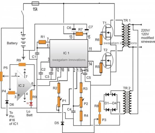
In one of the earlier posts I discussed the pin out functioning of the IC 3525, using the data, I designed the following circuit which is though quite standard in its configuration, includes a low battery shut down feature and also an automatic output regulation enhancement.
The following explanation will walk us through the various stages of the circuit, I have explained them:
As can be witnessed in the given diagram, the IC SG3525 is rigged in its standard PWM generator/oscillator mode where the frequency of oscillation is determined by C1, R2 and P1.
P1 can be adjusted for acquiring accurate frequencies as per the required specs of the application.
The range of P1 is from 100Hz to 500 kHz, here we are interested in the 100 Hz value which ultimately provides a 50Hz across the two outputs at pin#11 and Pin#14.
The above two outputs oscillate alternately in a push pull manner (totem pole), driving the connected mosfets into saturation at the fixed frequency - 50 Hz.
The mosfets in response, "push and Pull the battery voltage/current across the two winding of the transformer which in turn generates the required mains AC at the output winding of the transformer.
The peak voltage generated at the output would be anywhere around 300 Volts which must adjusted to around 220V RMS using a good quality RMS meter and by adjusting P2.
P2 actually adjusts the width of the pulses at pin#11/#14, which helps to provide the required RMS at the output.
This feature facilitates a PWM controlled modified sine waveform at the output.
Automatic Output Voltage Regulation Feature
Since the IC facilitates a PWM control pin-out this pin-out can be exploited for enabling an automatic output regulation of the system.
Pin#1 is the sensing input of the internal built in error Opamp, normally the voltage at this pin (non inv.) should not increase above the 5.1V mark by default, because the inv pin#1 is fixed at 5.1V reference internally.
As long as pin#1 is within the specified voltage limit, the PWM correction feature stays inactive, however the moment the voltage at pin#1 tends to rise above 5.1V the output pulses are subsequently narrowed down in an attempt to correct and balance the output voltage accordingly.
A small sensing transformer TR2 is used here for acquiring a sample voltage of the output, this voltage is appropriately rectified and fed to pin#1 of the IC1.
P3 is set such that the fed voltage stays well below the 5.1V limit when the output voltage RMS is around 220V. This sets up the auto regulation feature of the circuit.
Now if due to any reason the output voltage tends to rise above the set value, the PWM correction feature activates and the voltage gets reduced.
Ideally P3 should be set such that the output voltage RMS is fixed at 250V.
So if the above voltage drops below 250V, the PWM correction will try to pull it upward, and vice versa, this will help to acquire a two way regulation of the output,
A careful investigation will show that the inclusion of R3, R4, P2 are meaningless, these may be removed from the circuit. P3 may be solely used for getting the intended PWM control at the output.
Low Battery Cut-of Feature
The other handy feature of this circuit is the low battery cut off ability.
Again this introduction becomes possible due to the in built shut down feature of the IC SG3525.
Pin#10 of the IC will respond to a positive signal and will shut down the output until the signal is inhibited.
A 741 opamp here functions as the low voltage detector.
P5 should be set such that the output of 741 remains at logic low as long as the battery voltage is above the low voltage threshold, this may be 11.5V. 11V or 10.5 as preferred by the user, ideally it shouldn't be less than 11V.
Once this is set, if the battery voltage tends to go below the low voltage mark, the output of the IC instantly becomes high, activating the shut down feature of IC1, inhibiting any further loss of battery voltage.
The feedback resistor R9 and P4 makes sure the position stays latched even if the battery voltage tends to rise back to some higher levels after the shut down operation is activated.

Parts List
All resistors are 1/4 watt 1% MFR. unless otherwise stated.
- R1, R7 = 22 Ohms
- R2, R4, R8, R10 = 1K
- R3 = 4K7
- R5, R6 = 100 Ohms
- R9 = 100K
- C1 = 0.1uF/50V MKT
- C2, C3, C4, C5 = 100nF
- C6, C7 = 4.7uF/25V
- P1 = 330K preset
- P2---P5 = 10K presets
- T1, T2 = IRF540N
- D1----D6 = 1N4007
- IC1 = SG 3525
- IC2 = LM741
- TR1 = 8-0-8V.....current as per requirement
- TR2 = 0-9V/100mA Battery = 12V/25 to 100 AH
The low battery opamp stage in the above shown schematic could be modified for a better response as given in the following diagram:
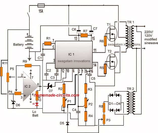
Here we can see that pin3 of the opamp now has it's own reference network using D6 and R11, and does not depend on the reference voltage from the IC 3525 pin16.
Pin6 of the opamp employs a zener diode in order to stop any leakages that might disturb pin10 of the SG3525 during its normal operations.
R11 = 10K
D6, D7 = zener diodes, 3.3V, 1/2 watt
Another Design with Automatic Output Feedback Correction
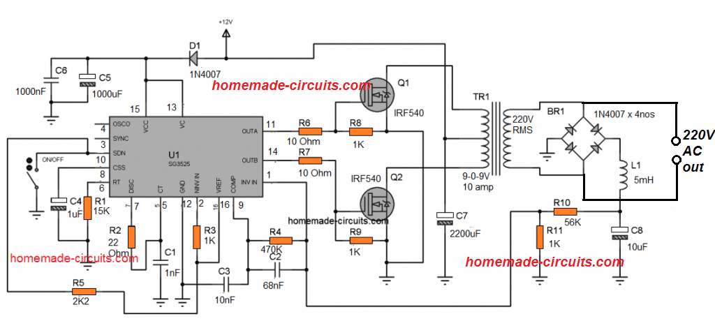
Circuit Design#2:
In the above section I have explained the basic version of IC SG3525 designed to produce a modified sine wave output when used in an inverter topology, and this basic design cannot be enhanced to produce a pure sine wave waveform in its typical format.
Although the modified squarewave or sine wave output could be OK with its RMS property and reasonably suitable for powering most electronic equipment, it can never match the quality of a pure sine wave inverter output.
Here I have explained a simple method which could be used for enhancing any standard SG3525 inverter circuit into a pure sine wave counterpart.
For the proposed enhancement the basic SG3525 inverter could be any standard SG3525 inverter design configured to produce an modified PWM output. This section is not crucial and any preferred variant could be selected (you can find plenty online with minor differences).
I have discussed a comprehensive article regarding how to convert a square wave inverter to a sine wave inverter in one of my earlier posts, here we apply the same principle for the upgrade.
How the Conversion from Squarewave to Sine wave Happens
You might be curious to know regarding what exactly happens in the process of the conversion which transforms the output into a pure sine wave suitable for all sensitive electronic loads.
It is basically done by optimizing the sharp rising and falling square wave pulses into a gently rising and falling waveform. This is executed by chopping or breaking the exiting square waves into number of uniform pieces.
In the actual sine wave, the waveform is created through an exponential rise and fall pattern where the sinusoidal wave gradually ascend and descend in the course of its cycles.
In the proposed idea, the waveform is not executed in an exponential, rather the square waves are chopped into pieces which ultimately takes the shape of a sine wave after some filtration.
The "chopping" is done by feeding a calculated PWM to the gates of the FET via a BJT buffer stage.
A typical circuit design for converting the SG3525 waveform into a pure sine wave waveform is shown below. This design is actually an universal design which may be implemented for upgrading all square wave inverters into sine wave inverters.
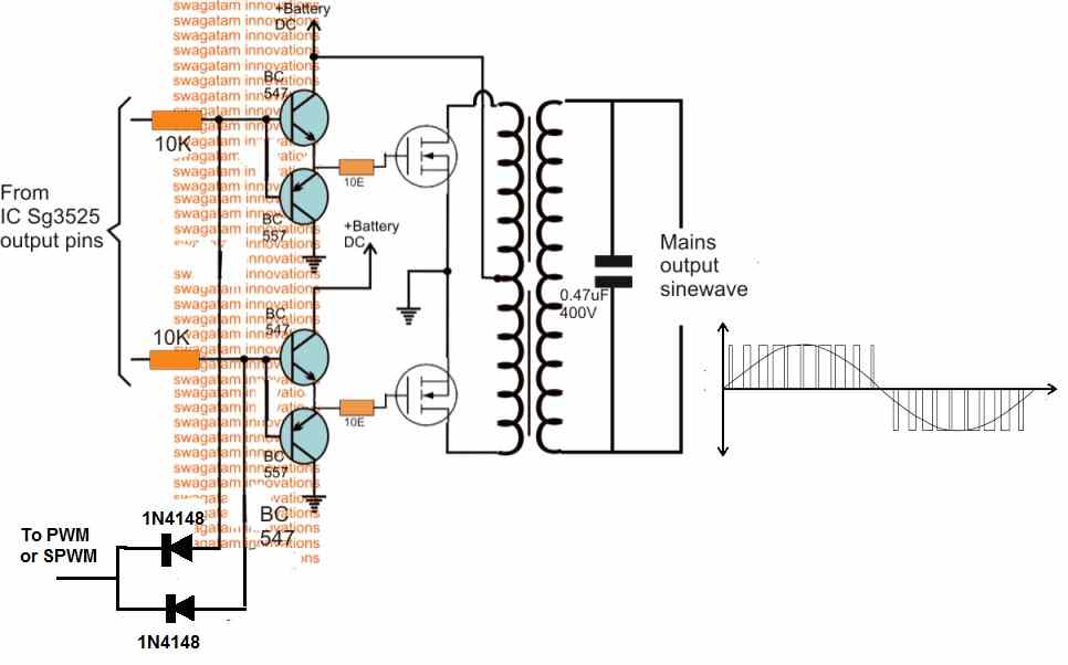
As may be in the above diagram, the lower two diodes are connected to a PWM feed or input, which causes the transistors to switch according to the PWM ON/OFF duty cycles.
This in turn rapidly chop the 50Hz pulses at the bases of the BC547/BC557 coming from the SG3525 output pins.
The above operation ultimately force the mosfets also to turn ON and OFF in the same pattern as the SPWM for each of the 50/60Hz cycles. This SPWM is then induced into the transformer primary by the MOSFETs, consequently producing a sine waveform at the output or the secondary side of the transformer.
If an ordinary PWM is used as I have explained below, then its frequency should be 4 times more than the base 50 or 60 Hz frequency. so that each 50/60Hz cycles are broken into 4 or 5 pieces and not more than this, which could otherwise give rise to unwanted harmonics and mosfet heating.
PWM Circuit
The PWM input feed for the above explained design can be acquired by using any standard IC 555 astable design as shown below:
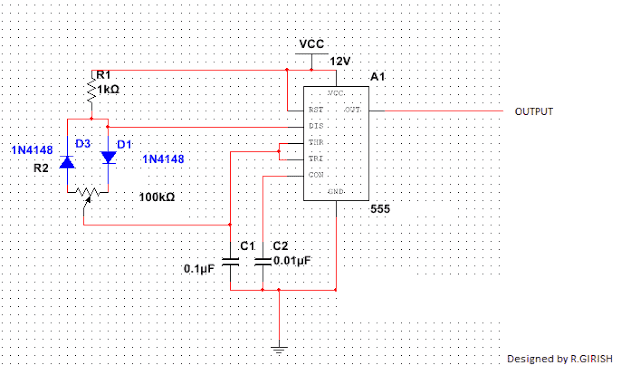
This IC 555 based PWM circuit can be used for feeding an optimized PWM to the bases of the BC547 transistors in the first design such that the output from the SG3525 inverter circuit acquires an RMS value close to mains pure sine wave waveform RMS value.
Using an SPWM
Although the above explained concept would greatly improve the square wave modified output of a typical SG3525 inverter circuit, an even better approach could be to go for an SPWM generator circuit.
In this concept the "chopping" of each of the square wave pulses is implemented through a proportionately varying PWM duty cycles rather than a fixed duty cycle.
I have already discussed how to generate SPWM using opamp, the same theory may be used for feeding the driver stage of any square wave inverter.
A simple circuit for generating SPWM can be seen below:
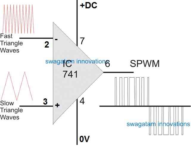
Using IC 741 for Processing SPWM
In this design we see a standard IC 741 opamp whose input pins are configured with a couple of triangle wave sources, one being much faster in frequency than the other.
The triangle waves could be manufactured from a standard IC 556 based circuit, wired as an astable and compactor, as shown below:
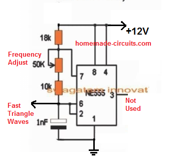
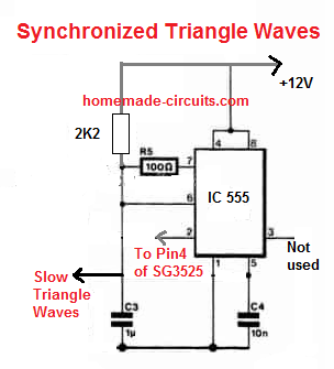
#UPDATE: The above "slow triangle waves" can be directly acquired from the Ct pin of the IC, that means you can now eliminate or ignore the above IC 555 stage for the slow triangle waves.
As can be seen in the above two images, the fast triangle waves are achieved from an ordinary IC 555 astable.
However, the slow triangle waves are acquired through an IC 555 wired like a "square wave to triangle wave generator".
The square waves or the rectangular waves are acquired from pin#4 of SG3525. This is important as it synchronizes the op amp 741 output perfectly with the 50 Hz frequency of the SG3525 circuit. This in turn creates correctly dimensioned SPWM sets across the two MOSFET channels.
When this optimized PWM is fed to the first circuit design causes the output from the transformer to produce a further improved and gentle sine waveform having properties much identical to a standard AC mains sine waveform.
However even for an SPWM, the RMS value will need to be correctly set initially in order to produce the correct voltage output at the output of the transformer.
Once implemented one can expect a real sine wave equivalent output from any SG3525 inverter design or may be from any square wave inverter model.
Finalized SG3525 Pure Sine Wave Inverter Circuit
The following diagram shows the finalized design of the pure sine wave inverter using IC SG3525 and SPWM, as per the above explanations.
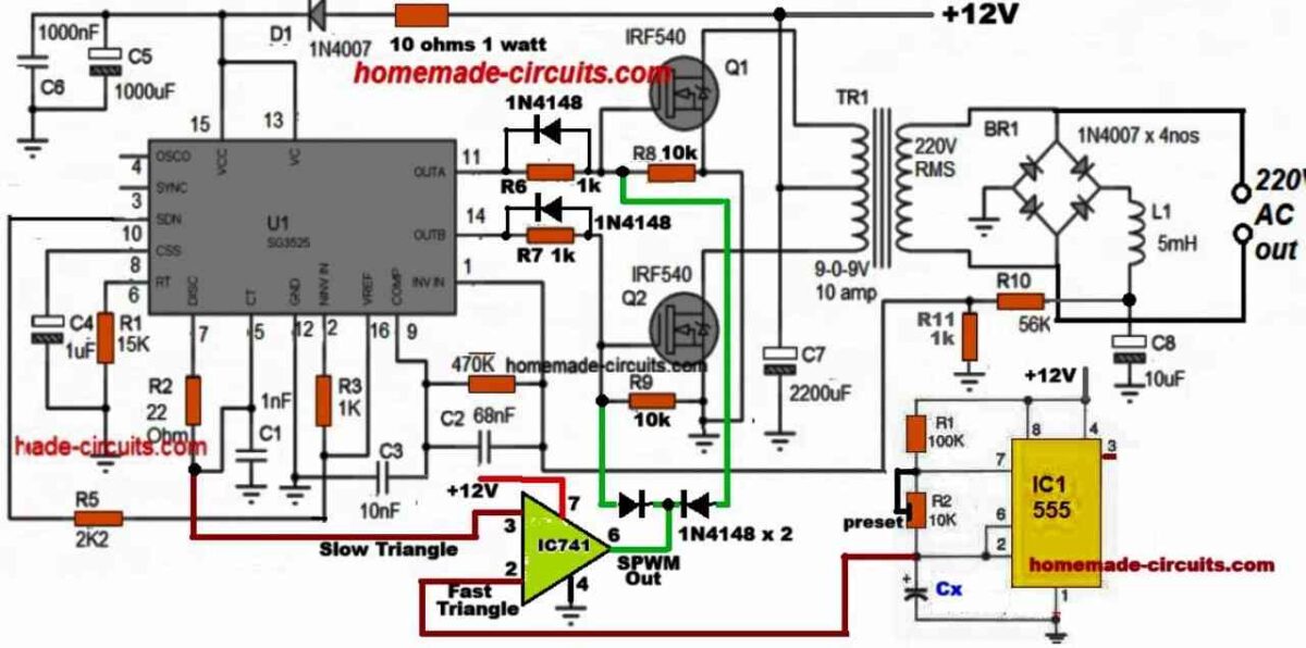
If you have any doubts regarding the above SG3525 pure sine wave inverter circuit you can feel free to express them through your comments.
UPDATE
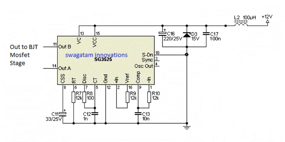
A basic example design of a SG3525 oscillator stage can be seen below, this design could be integrated with the above explained PWM sine wave BJT/mosfet stage for getting the required enhanced version of the SG3525 design:
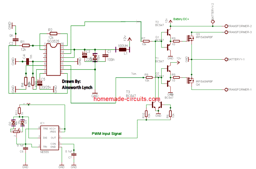
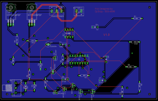
Complete circuit diagram and PCB layout for the proposed SG3525 pure sine wave inverter circuit.
Courtesy: Ainsworth Lynch
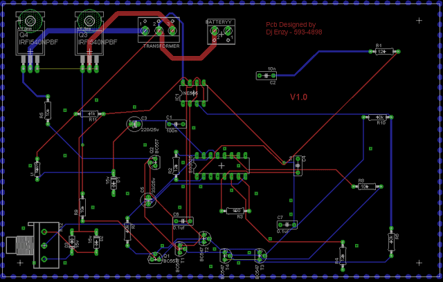
Design#3: 3kva Inverter circuit using the IC SG3525
In the previous paragraphs we have comprehensively discussed regarding how an SG3525 design could be converted into an efficient sine wave design, now let's discuss how a simple 2kva inverter circuit can be constructed using the IC SG3525, which can be easily upgraded to sine wave 10kva by increasing the battery, mosfet and the transformer specs.
The basic circuit is as per the design submitted by Mr. Anas Ahmad.
The explanation regarding the proposed SG3525 2kva inverter circuit can be understood from the following discussion:
hello swagatam, i constructed the following 3kva 24V inverter modified sine wave (i used 20 mosfet with resistor attached to each, moreover i used center tap transformer and i used SG3525 for oscillator).. now i want to convert it to pure sine wave, please how can i do that?
Basic Schematic
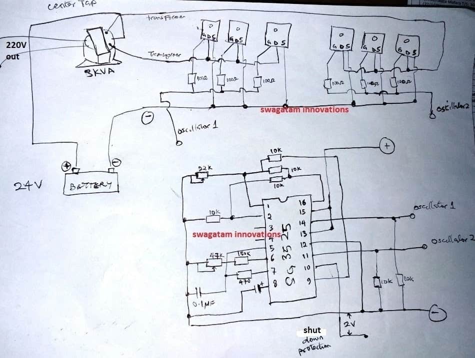
My Reply:
Hello Anas,
first try the basic set up as explained in this SG3525 inverter article, if everything goes well, after that you can try connecting more mosfets in parallel.....
the inverter shown in the above daigram is a basic square wave design, in order to convert it to sine wave you must follow the steps I have explained below The mosfet gate/resistor ends must be configured with a BJT stage and the 555 IC PWM should be connected as indicated in the following diagram:
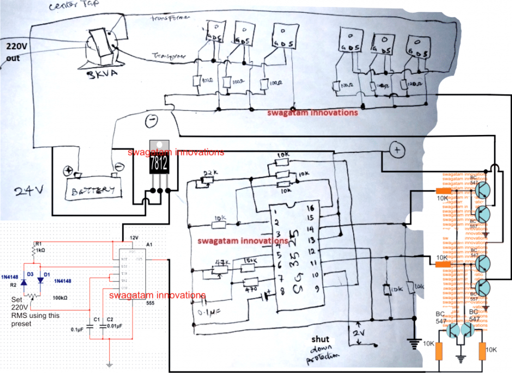
Regarding Connecting parallel mosfets
ok, i have 20 mosfet(10 on lead A, 10 on lead B), so i must attached 2 BJT to each mosfet, that's 40 BJT, and likewise i must connect only 2 BJT coming out from PWM in parallel to the 40 BJT? Sorry am novice just trying to pick up.
Answer:
No, each emitter junction of the respective BJT pair will hold 10 mosfets...therefore you will need only 4 BJTs in all....
Using BJTs as Buffers
1. ok if i may get you right, since you said 4 BJTs, 2 on lead A, 2 on lead B, THEN another 2 BJT from the output of PWM, right?
2. am using 24 volt battery hope no any modification to the BJT collector terminal to the battery?
3. i have to use variable resistor From oscillator to control the input voltage to the mosfet, but i don't know how i will go about the voltage that will go to the base of the BJT in this case, what will i do so that i want end up blow up the BJT?
Yes, NPN/PNP BJTs for the buffer stage, and two NPN with the PWM driver.
24V will not harm the BJT buffers, but make sure to use a 7812 for stepping it down to 12V for the SG3525 and the IC 555 stages.
You can use the IC 555 pot for adjusting the output voltage from the trafo and set it to 220V. remember your transformer must be rated lower than the battery voltage for getting optimum voltage at the output. if your battery is 24V you can use an 18-0-18V trafo.
Parts List
IC SG3525 Circuit
all resistors 1/4 watt 5% CFR unless otherwise specified
10K - 6nos
150K - 1no
470 ohm - 1no
presets 22K - 1no
preset 47K - 1no
Capacitors
0.1uF Ceramic - 1no
IC = SG3525
Mosfet/BJT Stage
All mosfets - IRF540 or any equivalent Gate resistors - 10 Ohms 1/4 watt (recommended)
All NPN BJTs are = BC547
All PNP BJTs are = BC557
Base Resistors are all 10K - 4nos
IC 555 PWM Stage
1K = 1no 100K pot - 1no
1N4148 Diode = 2nos
Capacitors 0.1uF Ceramic - 1no
10nF Ceramic - 1no
Miscellaneous IC 7812 - 1no
Battery - 12V 0r 24V 100AH Transformer as per specs.
A Simpler Alternative
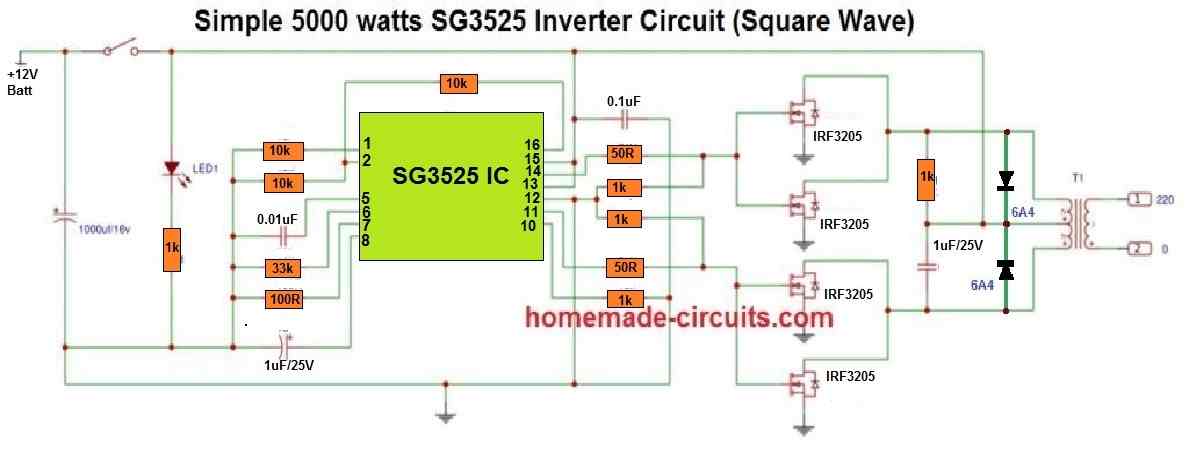

sir is one of 1uf 400v okay or should i add three in parallel
You can use 1, 2 or 3 until the output shows a near clean sine wave.
Please is it must that I connect 0.47uf 400v in the output of the transformer
You can use 1uF/400V also.
Sir but in some of your circuit you use pin 3 of the op amp ic as the fast traingle but in this circuit you use pin 3 of the op amp ic as the slow triangle
John, connecting slow triangle to pin#3 is the correct method, so you can follow this.
Sir please should i connect pin 3 of the op amp ic to pin4 of the sg3525
You can connect the opamp pin#3 to pin#5 (Ct) pinout of the SG3525…but remember you must have an oscilloscope to verify all these waveform before finalizing the SPWM output.
Sir that ic 555 timer circuit for fast traingle. What resistor should i add to get 50hz instead of using 50k pot
John, you will have to experiment the values using a frequency meter. Or you use any 555 astable online calculator to calculate the values for getting 50 Hz output.
Please sir one more last question can i connect pin 4 of the op amp ic to negative terminal of the battery
Yes you can, the plus and minus signs for the op amp pin 7 and pin 4 refers to the battery positive and negative terminals.
Sir please where will I connect the pin 2 and 3 of the ic741
To slow and fast triangle waves from the 555 astable circuits.
Sir what if i try that second to the last circuit will it match pure sine wave
You will have employ the op amp SPWM integration with the MOSFET gates of the SG3525 circuits in order make then into pure sine wave inverters.
Please sir is that design:2 suitable for CRT televisions
It won’t be suitable unless it is a pure sine wave. You can try the following designs instead:
Arduino Pure Sine Wave Inverter Circuit with Full Program Code
1500 watt PWM Sinewave Inverter Circuit
Can I use irf3205 instead of irf540 ???? and is it suitable for powering CRT television???
Yes, you can use IRF3205 instead of IRF540.
Ing. I want it to be sinusoidal and self-regulated,,, tell me Ing: what changes would I make to this circuit so that my case for 220v is self-regulated.
https://www.homemade-circuits.com/wp-content/uploads/2017/06/sg3525-2.png I
could extract the circuit from this schematic, just the self-regulating part.
http://radioaficionado.dynu.net/inversor/PWM-inverter-circuit.png
1- Doubt …what to put in Shut down protection 2v
NOTE: or only the SG3525 has for self-regulation. If so, add that I do it… All your circuits worked for me,,,,
Thanks Felix,
you can try the first circuit from the following article:
https://www.homemade-circuits.com/inverter-circuit-with-feedback-control/
Pin#10 can be used for low battery shut down or something similar.
For sine wave output you will have to employ the op amp technique which is explained in the above article.
ing, creo que no necesitaría osciloscopio para ajustar la frec de estos diseños,,?,,se podría ajustar con un multitester que tenga para medir frecuencia..?
1…https://www.homemade-circuits.com/wp-content/uploads/2019/04/sg3525INVERTERCIRCUITWITHOVERLOADLOWBATTPROTECTIONCIRCUIT.jpg
2..https://www.homemade-circuits.com/wp-content/uploads/2016/08/SG3525-with-IC555.png
Tengo entendido que los 2 diseños so de onda sinusoidal pura..?
Sorry, these are not sine wave inverters. You can convert these designs into a sine wave by adding the following stages to the mosfets:
https://www.homemade-circuits.com/wp-content/uploads/2022/08/SPWM-connection-with-mosfets.jpg
https://www.homemade-circuits.com/wp-content/uploads/2022/07/how-to-generate-SPWM-using-IC-741.jpg
Hi . I want to make a PiezoEelectric Driver that needs 19-25V as a input voltage and the range of 100~800V as a output voltage . and also the range of output frequency should be variable at 5Khz~100Khz . the output wave must be sinwave . i want to use SG3525 and a boost topology such as push pull and … with transformer and at the end i want to use a filter to make a sinwave . but my problem is it works only in specific operation frequency and with changing the RT ( for adjust the frequency ) the output voltage is not pure sin . what should i do ?
I must use several filters and select that with appropriate operation frequency ? for example use Arduino to diagnosis the operation frequency and consistent with it the output filter would be selected
Hi, SG3525 cannot be used to create a pure sine wave inverter with filters, unless an external sine PWM is applied. Instead, you can use the following Arduino concept for the sine wave generation. However, this circuit uses 50 Hz frequency with an iron core transformer. You may have to suitably modify the frequency and the transformer for 100 kHz operation:
Arduino Pure Sine Wave Inverter Circuit with Full Program Code
Hlw sir what is the value of pin number 8 in that circut of 3kva circuit
Pin#8 capacitor is for initiating a soft start at the output of the inverter. You can use any capacitor between 0.1uF and 1uF
Good day Sir, Chief Swag, please can op amp voltage follower do the work of btj buffer stage of the oscillator?
Yes op amp voltage follower can be used instead of the BJT buffer.
Thanks so much Swagatam for your reply, please my concern is how to protect this in case of positive and negative line bridging.
Without buffer stage, bridge does not damage the inverter.
However, buffer stage is essential.
Thanks Swag.
Hello Seun,
Buffer stage is not essential. If you are referring to a SG3525 circuit you can connect the mosfets directly with the output pins.
I did not understand what you want you protect? If you short circuit a battery only a fuse can protect the battery.
Good day Swag, I tried the op amp lm324 voltage follower, from 3.5v from each output pins, it increased to 8v. When connected to both gates, it blew the MOSFETs.
Please Sir, what can I do to use as buffer stage.
Thanks.
Good day Seun,
How much voltage did you use for the SG3525 IC?
If you use 12 V for the SG3525 IC then no op amp would be required for the MOSFETs?
Moreover a voltage follower will never boost a voltage level fro lower to higher.
There is something else that I need to understand. In other inverter drawing I have seen resisitance and diodes connected to gate of mosfet for protection. Is there any unprotection comparing your schematic with the one that use those diodes?
Yes, the diode across the gate resistance facilitates better and efficient conduction of the MOSFETs and lower heating of the MOSFETs.
Hi Swagatam, in my country we use 60Hz apliances. Regarding the first and second schematic, by P1 can I set 60Hz and use it without operation problem.
Is there something else to be minded if I increase number of mostfet to get more power?
Hi Neybero,
I would recommend you the following circuit instead, since it is a simpler one and has been tested. You can tweak the R1/C1 values to get the required 60 Hz output
https://www.homemade-circuits.com/wp-content/uploads/2019/04/feedback-1024×460.png.webp
Thank you for responding. As electronic hobbilist I am not experience in electronic design.
To be sure. For frequency you say R1-C1, is it right or R2-C1, R1-C4?.
I am sorry if I bother you with my unexperience.
Only R1 and C1 are responsible for the output frequency of the inverter and only these must be adjusted.
Hello Swagatam,
Please I have seen an inverter designed as PWM module from the internet, and this is not from your posts, using the Sg3525 IC.
It has this features, Overload protection, low battery shut down, automatic cooling fan. This is only, the oscillation board, with each pin of these functions out.
Since you said we could bring to you at times some of these to discuss, I would like to know where to in the circuit when I am adding a transformer 50hz and power mosfets to complete the design, I should connect the overload pin and low battery shut down pin.
Hello Ekoe,
Please refer to the first circuit from the above article, and connect the mosfets and the transformer exactly as shown the diagram.
Hello sir..I want to made this project can you tell me which circuit suitable for me with output voltage feedback.. and any modification will required or not.
Hello Apurv,
All the circuits are good, but you can specifically try the following design with a feedback:
https://www.homemade-circuits.com/wp-content/uploads/2019/04/feedback-1024×460.png.webp
Ok sir.one more question is that if added mosfet driver (totempole driver) in pin 11 and 14 for increasing the output current to drive more mosfet .then any modification will happen in your given cricuit or not…
According your CT,RT,RD value is given in your cricuit digram by the formula(1/CT(0.7Rt +3Rd).I calculated then coming frequency is 94khz but my requirement is 50hz how it can be occurred..
Please clear my all point thank you..
Hello Apurva,
Driver is not required for adding MOSFETs in parallel, you can add the MOSFETs in parallel directly with the pin#11 and pin#14 of the IC. No modifications will be required.
In the formula did you convert microfarad into Farad? You will have to convert microfarad into farad for getting the correct results.
If the formula is not giving proper results then it is better to confirm the frequency practically using a frequency meter.
Yes sir I firstly converted into farad then i calculated it but the result came same (94643hz).so please give me a correct value of CT,Rt and Rd which I can used in my project because it’s my college project for demonstration purpose.and one more question is that if I can used mosfet driver cricuit then I think no any problem will create.if I am right.
Thank you and waiting for your response..
Hi, Apurv,
your calculations are correct. So I will suggest you to please try increasing the RT value until you get the approximate 50 Hz frequency.
It can be difficult for me to do the calculations for you due to lack of time.
Hello sir, in my calculation I used CT,RT,Rd is(0.1uf, 150k (100k preset and 50k Resistance) ,47ohm) when i set into the 133k the total frequency is 104hz comes out after calculation.so please verify my it’s correct or not and one more thing also I want know that the pin #11 and pin#14 their total sum frequency will be calculated or not. because the frequency perivouslly I measured is total frequency.
So please rply me sir…I working on this project
Apurv, as I told you before due to lack of time I cannot confirm the calculations. You can confirm it by testing the real results with a meter.
One half cycle from pin#11 and one half cycle from pin#14 constitutes one full cycle of the output frequency of the inverter. You can measure the 50 Hz frequency by attaching the meter probes across pin#11 or pin#14 and ground. Or you can connect the meter probes across pin#11 and pin#14 to check the 50 Hz frequency.
Your rply is important for me sir.if you can do immediately then I work on project very smoothly perfectly so please rply me sir….
Apurv, I am not always online, therefore my replies can be within 1 hour or sometimes 12 hours.
Hello sir I requested to you please concern my msg and immediate reply me…thank you
Hello sir please reply my comments..I am waiting your answer.
Dear swagatam. Thanks for the good works you are doing on this space.
I designed a 24v 1.5kva H-Bridge inverter using SG3524.
So far it is working fine.
I have used a pressing iron of 1200watts on it and it operates fine.
My challenge is on inductive loads. My freezer of 120watts couldn’t start on it.
It works on my fan but it’s giving off a humming sound and it doesn’t run on full power.
I guessed it is because of the inverter being a modified sinewave.
How can I eliminate this problem?
Would putting a capacitor of say 1uf or 1.5uf at the output of the inverter help?
Any idea on what to do?
That’s wonderful Gabriel, Glad you could build a full bridge inverter successfully.
Freezer might require high current during initial switch ON loading. A 120 watt unit could consume around 400 watts at the start. That is why your inverter might be having difficulty in handling the freezer. You can try upgrading your inverter to 600 watts and then check the results.
Yes you can add a 3uF/400V capacitor across the output terminals of the inverter in order to reduce the noise to some extent.
SG3524 inverters are normally square wave inverters so tackling the noise may not be easy.
Hullo friend I have fridge it’s lebled 150watts but have tried an invert of 600watts but it doesn’t work can you advice me the circuit that can start it. Thanks
Hi, if you built the 600 watt inverter correctly then it should be able to operate the 150 watt inverter with ease.
Your inverter might not be actually rated at 600 watts.
good morning, I would like to know if this circuit for sine wave air to use in an inverter that does not use an iron transformer, so used in a high frequency inverter in the first stage and a bridge – H in the second stage?? I’ve been reading your post, and I want to thank you for making your knowledge available!!!
Hi, this circuit can be customized for a ferrite based transformer by increasing the oscillator and PWM frequency to many kHz. However, the designing of the ferrite core transformer would be crucial and will need to be done with a lot of calculations.
I am glad you are finding my posts helpful.
Thanks Mr Swagatam for the reply.
Good morning Swagatam,
I’ve built almost your sg3525 design from this post, the simple ones, only inverter number 1 and 2, I couldn’t build that I’ve found complex very little.
Now about the design number 1, the first from this post, the i.c lm371 for the low battery circuit, pin#7 of the circuit are not connected to the whole system. Please, where do they go to the inverter circuit if I would try to build this. Please where do these two pins connect to?
Hello Ekoe,
The low battery cut off op amp is a 741 IC. The pin 7 and pin 4 are its supply voltage pins which will need to be connected with the battery supply if the battery is a 12V battery. Pin7 will go to the (+) of the battery, and pin4 to the (-) of the battery
Hello Swagatam,
I’ve decided to use my inverter project build in their square wave form, your design, sg3525 3kva and the sg3525 5000watts square wave. And I wish to use these two mosfets, irf 3205 and irfz 44n, which are common at my place and affordable. Do I need any change of the gate resistances ? If so, which of them do I have to look for, for the two inverters of your design, please. My fundamental knowledge in electronic is few so often my questions.
Hello Anthony,
You can try the 3rd circuit from top. It is simple and compact. Build with a single mosfet first. If you succeed with it, then you can add more number mosfets in parallel to increase its wattage.
Hello Swagatam,
Thanks for the reminder of the oscilloscope, now I built the Spwm, the fast triangle waves your design, with the Ne555 i.c.
Adjusting the preset 50k, I got the
400hz as you indicated in your posts after my persistent trials.
Please did say if I connect I suppose to still get my 50hz oscillating normally from pin #11 and #14 that will drive the power mosfets?
Hello Anthony,
As mentioned earlier, to proceed with the SPWM section you must have the following two things with you:
1) A basic SG3525 inverter producing 220V AC output at 60 watt or more
2) An oscilloscope to check the waveform.
Without these two you cannot verify the SPWM stage
Hello Swagatam, I have built the basic square wave of sg3525 already. It’s just unfortunate that I don’t have the oscilloscope. Thanks for your advice.
Hello Anthony, the inverter should be complete and produce 220V output and able to illuminate a 60 watt lamp. oscilloscope will be required for the SPWM integration.
Hello Swagatam,
Please may I suggest if you could demonstrate some of the sg3525 inverter circuit to us through a video in the YouTube.
I had built and tested this circuit long back about 10 years ago, and it worked perfectly for me. It won’t be possible for me to build it again and make a video, that will be a lot of hard work.
If you are finding the circuit difficult then you should first try the basic square wave SG3525 circuit and then upgrade it into a sine wave inverter step by step.
You must have a small oscilloscope to test the waveform otherwise building the inverter correctly may not be possible.
Hello Swagatam,
Do I need any polirise capacitor on the battery positive line going to the Power regulator ic 7812 which feeds the main oscillator i.c Sg3525 of the inverter circuit. If so which value do you recommend to me.
Secondly the two diodes of the PWM were turned upside down, could please explain to me why. I know diode has only one passage . Please thanks.
Hello Anthony,
you can use a polarized capacitor before and after 7812. You can use a 100uF/50V capacitor. The diodes pull down the transistor bases to 0V for all the 0V pulses of the PWM cycle, in this way it forces the transistors to switch ON/OFF exactly in accordance with the PWM pulses.
Please Swagatam, again I didn’t connect my shut down line from pin #10, what will happen to my inverter if I don’t do so. The role of the feed back? Is not added to the sg3525 of 3kva inverter circuit.
You can keep the pin#10 connected to ground initially. Feedback (220V constant output) can be added only when the basic inverter circuit works correctly.
Hello Engineer,
My final struggle and the results, I finally finished the oscillation board, setting my preset 47K, I got 03.80volts d.c. and 50hz at the two pins 11&14.
Setting up the preset 22K, I increase the d.c voltage at the two oscillations to 05.08&05.07 each.
I build the PWM circuit and the frequency I got was 247.7Hz.
Connecting the two overheat all the BJT transistors on the oscillation lines. And result is giving negative 200-300mv d.c and unstable, there I was afraid to destroy my transistors, I did not connect any of my power transistors. I used the conversion design with the two 10K and 547.
Thanks that you at last replaced it with the two diodes.
What suppose to be the d. c voltage that would drive the power transistors if all the circuit is set and also the oscillator frequency if the PWM is connected?
Hello Anthony,
Do not use the PWM initially. First build the basic SG3525 inverter and test the results. If you get 220V AC perfectly from this inverter only then proceed with the PWM.
If you try to build the whole circuit all at once then you may face serious problems. You must build the circuit stage-wise.
And please remember without an oscilloscope you cannot succeed with the PWM integration.
Thanks Swagatam, Please the design circuit that convert the sg3525 into a sine wave, one has two transistors 547 and at each base is connected 10k ohms resistors, another you put recently has only two diodes 1N 4148 in the inverse way. Which of the two should be applied for the conversion stage. Thanks
Hello Anthony,
The design using two BC547 could not be used for SPWM that is why I changed the previous diagram with a new diagram which has two diodes instead of two transistors. This new design with two 1N4148 diodes can be used universally with ordinary PWM and also with SPWM
Hello Good morning, Please how do I connect the shut down line from pin#10 of the sg3525 3kva design. Is it going to be used as switch between battery plus and minus in the circuit or how please direct me.
If you are not using an automatic feedback for the shut down then you can keep the pin#10 connected with the ground line. This will keep the shut down feature disabled.
Hello Mr Swagatam, thanks for alerting me, I waisted my energy all this while. Okay I am building your 3kva of your design and I will inform you of the results if am done.
Sure, no problem.
Hello big man, Honestly I am not doing anything different from what you continue to instruct me. I am using the Ainsworth Lynch sg3525 diagram, so, where in the circuit of the ne 555 timer, pin#3 is used to feed the sg3525 two transistors 547, they connect the two oscillation lines of the sg3525 circuit in the inverter diagram, Yes exactly I did, the pin#5 of sg3525 of my construction replaces the feeding pin #3 of the Ne555 timer in your drawing. Am surprised.
Hello Anthony,
I think you are getting confused
The Ainsworth Lynch circuit will not provide pure sine wave output.
Pin#5 of SG3525 has no role in Ainsworth Lynch circuit.
Pin#5 of SG3525 is an option which can be used for getting slow triangle waves for the op amp cirucit
Hello my instructor, I connect pin#5 of sg3525 to the two transistors for the conversion stage only to see that there is no oscillation at the output of pin#11& pin#14, my meter reading is 0.000and the voltage reading is 0.441volt very bad results. Am really down for my result. Well I am not an electronic product so the difficulty. Thanks for the advice to acquire the handset oscilloscope. I always do well to build the oscillation circuit for every simple inverter that I find. But if you could endure me to complete one of the sg3525 of your simple sine wave inverter I would be grateful. I don’t know where exactly I am lacking in. Thanks big man.
Pin#5 of SG3525 is an option which can be used for extracting the slow triangle waves and can be used at the op amp pin#3.
Pin#5 generates the slow triangle waves.
Hello Swagatam, Yes I have got 50hz at pin #11 as well as pin #14 really. But unfortunately I don’t have the oscilloscope, only my small multimeter. But thanks for confirming the 90hz, I will connect to see the behavior of the oscillation at pin #11. If my 50hz do not change then I can connect my power transistors. But if you have something very important to advise me about you are very welcome, am very excited myself even though I have not finished. I I even followed you up to YouTube, Thanks again.
Hello Anthony,
You can use the 90 Hz as the slow triangle waves, it will not affect the sg3525 output frequency.
If you don’t use an oscilloscope then you will not be able to confirm the waveform and the results. How will you check the SPWM generation?
You can easily purchase a small hand held oscilloscope such as the DSO138 which is very cheap and accurate.
Thank you for subscribing to my You tube channel,
Hello Swagatam, I built the oscillator circuit of the sg3525 your design. But at pin#5 as you indicated, the frequency there is more than 50hz, it’s around 90hz plus. And pin#4 is 100hz. You said we need 50hz for slow spwm which we must feed the two 547 transistors. Now what next should I do for the result that I’ve got for my inverter that I am building, please help me out.
Hello Anthony,
What frequency are you getting at the output pin#11 and pin#14 of the IC? If it is around 50 Hz, then 90 Hz from pin#5 is fine you can use that for the slow triangle waves.
But remember you will need an oscilloscope for checking all the relevant waveforms otherwise it will be impossible for you to confirm the results.
Hello Swag, Please from the standard ic 555 design of the spwm, the fed arrow pins 6&2 of the fast triangle wave is one likewise the pwm design. But the slow triangle wave design has two arrows from 2 pins respectively. Slow triangle wave from pin 6, now where do the one from pin 2 goes to in the construction? By your indication it goes to pin 4 of the sg3525 with the arrow pointing. Supposing I am using this design do I necessarily connect the two pins 6 and 2 of the ic by the arrows directions. I am asking this in the case of the slow triangle wave of the spwm of the ic 555, should one want to use this design. Consider me for my bothering contents, thanks engineer.
Hello Anthony,
Yes that’s correct, you must do exactly as indicated in the slow triangle wave diagram. This is to ensure that SPWM cycles are exactly in sequence with the 50 Hz frequency cycles of the SG3525. However you can eliminate this 555 stage entirely and get the synchronized slow triangle waves directly from pin#5 of SG3525 which we have already discussed in the previous comments.
Hello Swagatam, I have been trying to realize this sg3525 simple sine wave inverter but was having a problem with the conversion by using the ic 555 circuit before I left. Now reading through over and over I’m having a bit understanding now. Please by your explanation if you use the SPWM circuits, fast and low, the low must have the same frequency 50hz with the main ic sg3525 right. Now if I use your configuration exact will I be able to get a the 50hz or I have to change the capacitor. I asked because I don’t know how to calculate it. And again what’s the Ct you talked about on ic 555 circuit? I am mechanic but love inverters circuit diagram that are not complicated.
Hello Anthony, yes the slow triangle wave must be 50 Hz or at the frequency that is required at the output of the transformer.
However, this slow frequency must be synchronized with the SG3535 frequency so that the op amp is able to create the exact set of SPWM matching the period of the mosfet ON time.
Therefore in order to synchronize the SPWM with the mosfet switching we can extract the 50 Hz slow triangle from the “Ct” pin of the SG3525. The pin#5 of the IC SG3525 is the Ct pin
Thanks for prompt response, God bless you
Thanks for your prompt response, God bless you. Then it means after I have realized the sg3525 main circuit with my 50hz at the two pins 11&14 of the sg3525. Now I can connect from the pin no. 5 of the main ic sg3525 to the two 547 transistors for conversion for my sine wave for my inverter, is that what you mean?
No that is not correct. The 50 Hz from pin#5 must be connected to the to the op amp (+) input where the slow triangle waves is suppose to be applied.
Good day Sir, Swag, please what can I do to my sg3524 inverter system, when I power freezer at 220v, it works fine but inverter hums.
Hi Seun,
the humming could be due to overloading of the inverter, you can try using a bigger transformer and see if that solves the problem. To confirm this check the transformer temperature while the freezer is working…if the transformer is getting hotter then surely the problem is due to overload.
OK Sir, thanks. Could bjt buffer stage help?
BJT buffer might not be related to the problem. Th issue could be either due to overloading or due to crude waveform from the inverter.
I noticed at 180v quiet even on loads, but at 215v above it gives a loud sound, anything to do, Sir
Higher voltage will mean more current drawn by the load which can create overloading on the transformer causing vibrations in the transformer and noise. Check the output voltage without the load connected, it could be a lot higher than 215V. You can try adding a capacitor across the transformer output wires and see if that helps.
I noticed that at 175v it is quiet and was able power the freezer and gets colder fast than 215v, please why this better efficiency at this voltage.
However, when powered with TV there are moving lines on it.
Please what can be done.
Thanks.
Not exactly sure, maybe the fridge coils get hotter at 215 V causing inefficient cooling.
The moving lines are due to harmonics in the inverter output waveform. Try adding a capacitor across the inverter output and see if that helps.
I have an inverter 1.5kva/24v factory design, used with 150ah battery, the charging setting. Says c6-c3, which one is safe
I am not sure what c6, c3 means.
So sir when the dead time resistor is correctly fixed he do I know
It is not critical….By default there will some deadtime even if you don’t connect the external resistor. If you add a resistor that will increase the deadtime….Check the output average DC across the output, it should not be less than 40% of the battery voltage, this will prove an optimal deadtime value….or you can also check it with a oscilloscope. Remember higher deadtime will decrease the output inverter voltage proportionately.
One more thing sir,how is the dead time resistor calculated and also what’s the function of p4 in the first design
I don’t have the formula for the dead time resistor. You will have to fix it by trial an d error by measuring the average DC across the output pins. With minimum dead time the voltage across the output pins will be almost equal to 50% of the battery DC…this will becomes lesser and lesser as the dead time is increased. P4 ensures that when the battery voltage reaches its low battery level the opamp output becomes high and latches. This latch breaks and the opamp output turns low again only when the battery is charged to a reasonably good position.
You can remove P4 and the series R9 resistor if you want, they are not too important.
Hello sir, which of the ic741 needs the fast triangle wave ,pin 3or2
Hi Melvis, the fast triangle wave should be on pin#2
I need to know dead time for full bridge or 3525 IC dead time used for full bridge . Also how to do Transformer design Full Bridge ?? any application note ???
can any one help me ??? 1200w full bridge transformer design using 3525
A resistor connected across pin#7 and pin#5 determines the dead time of the IC.
Do you want to connect a transformer to a full bridge circuit?
Hi,
Thanks for publishing such a nice project. I have a mind to construct the same if I can procure all the components online because the place where I live in is a remote one and it is hard to find all the components locally. Regarding automatic correction feature I have a question, once the voltage at pin2 is set through preset P2 is there any chance of increase/decrease this voltage as explained ? Rather the voltage at pin1 will increase/decrease as per output voltage. As you have explained Would you please explain it a bit more.
Hi, thanks and glad you liked the project! Once the automatic correction is set, the output voltage will remain constant and will not rise above the set threshold. However, if the load increases beyond the capacity of the inverter then the voltage might drop below the set threshold since the inverter will be unable to supply extra power to the load due to lack of transformer and battery power. So voltage will not rise beyond the set threshold this is guaranteed, but the voltage will not drop is not guaranteed.
Hi, my name is anil . I need a high frequency inverter for a research i am conducting. Can you plz send me the schema of your circuit. Otherwise, is there another way to have your circuit schema or your prototype ?
Hi Anil, you can try the last circuit shown in the following article:
https://www.homemade-circuits.com/half-bridge-mosfet-driver-ic-irs21531d/
Hello Sir, please how can I incorporate self charging system to my inverter without draining,
Seun, you can use one of the circuits from the following article to get an automatic charging cut offs:
https://www.homemade-circuits.com/opamp-low-high-battery-charger/
Hello Mr. Swagatam,
First of all thank you very much for your work.
I have some questions, I’m looking for a simple sine wave schematic for 25v – 230v 50Hz 1500w with feedback.
I don’t know if it will be valid to change Design#3
Can you help me please?
Thank you so much.
Hello Ricardo, you can use Design#3 to create a sine wave inverter, however, the mosfet gates will need to be chopped using SPWM for achieving the intended sine wave output.
Hello Mr. Swagatam,
Thanks for you replay.
Sorry i have some more questions, can i use P75NF75 mosfets?
How many will be needed for a power of 1500W?
Thank’s for your time.
Hello Ricardo, you can use 2 mosfets in parallel on each channel if the battery is 24V.
Good day sir thanks for replying to my earlier comments.please the question I want to ask is about ups
I noticed that my ups power output is about 600w instead of around 800w. Is there a way to increase the power factor
Thank you very much
Hello Bode, to increase the wattage capacity of an inverter you will have upgrade its transformer, battery and the mosfets appropriately. To improve power factor you may have to use a full bridge inverter instead of a center tap inverter
Calculate Battery, Transformer, MOSFET in Inverter