In this post I have explained a 3 powerful yet simple sine wave 12V inverter circuits using a single IC SG 3525. The first circuit is equipped with a low battery detection and cut off feature, and an automatic output voltage regulation feature.
This circuit was requested by one of the interested readers of this blog. I have explained more about the request and the circuit functioning.
You may also want to read how to design a sine wave inverter from the scratch.
Design#1: Basic Modified Sine
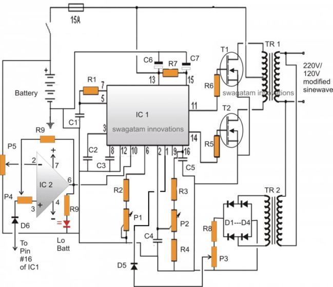
In one of the earlier posts I discussed the pin out functioning of the IC 3525, using the data, I designed the following circuit which is though quite standard in its configuration, includes a low battery shut down feature and also an automatic output regulation enhancement.
The following explanation will walk us through the various stages of the circuit, I have explained them:
As can be witnessed in the given diagram, the IC SG3525 is rigged in its standard PWM generator/oscillator mode where the frequency of oscillation is determined by C1, R2 and P1.
P1 can be adjusted for acquiring accurate frequencies as per the required specs of the application.
The range of P1 is from 100Hz to 500 kHz, here we are interested in the 100 Hz value which ultimately provides a 50Hz across the two outputs at pin#11 and Pin#14.
The above two outputs oscillate alternately in a push pull manner (totem pole), driving the connected mosfets into saturation at the fixed frequency - 50 Hz.
The mosfets in response, "push and Pull the battery voltage/current across the two winding of the transformer which in turn generates the required mains AC at the output winding of the transformer.
The peak voltage generated at the output would be anywhere around 300 Volts which must adjusted to around 220V RMS using a good quality RMS meter and by adjusting P2.
P2 actually adjusts the width of the pulses at pin#11/#14, which helps to provide the required RMS at the output.
This feature facilitates a PWM controlled modified sine waveform at the output.
Automatic Output Voltage Regulation Feature
Since the IC facilitates a PWM control pin-out this pin-out can be exploited for enabling an automatic output regulation of the system.
Pin#1 is the sensing input of the internal built in error Opamp, normally the voltage at this pin (non inv.) should not increase above the 5.1V mark by default, because the inv pin#1 is fixed at 5.1V reference internally.
As long as pin#1 is within the specified voltage limit, the PWM correction feature stays inactive, however the moment the voltage at pin#1 tends to rise above 5.1V the output pulses are subsequently narrowed down in an attempt to correct and balance the output voltage accordingly.
A small sensing transformer TR2 is used here for acquiring a sample voltage of the output, this voltage is appropriately rectified and fed to pin#1 of the IC1.
P3 is set such that the fed voltage stays well below the 5.1V limit when the output voltage RMS is around 220V. This sets up the auto regulation feature of the circuit.
Now if due to any reason the output voltage tends to rise above the set value, the PWM correction feature activates and the voltage gets reduced.
Ideally P3 should be set such that the output voltage RMS is fixed at 250V.
So if the above voltage drops below 250V, the PWM correction will try to pull it upward, and vice versa, this will help to acquire a two way regulation of the output,
A careful investigation will show that the inclusion of R3, R4, P2 are meaningless, these may be removed from the circuit. P3 may be solely used for getting the intended PWM control at the output.
Low Battery Cut-of Feature
The other handy feature of this circuit is the low battery cut off ability.
Again this introduction becomes possible due to the in built shut down feature of the IC SG3525.
Pin#10 of the IC will respond to a positive signal and will shut down the output until the signal is inhibited.
A 741 opamp here functions as the low voltage detector.
P5 should be set such that the output of 741 remains at logic low as long as the battery voltage is above the low voltage threshold, this may be 11.5V. 11V or 10.5 as preferred by the user, ideally it shouldn't be less than 11V.
Once this is set, if the battery voltage tends to go below the low voltage mark, the output of the IC instantly becomes high, activating the shut down feature of IC1, inhibiting any further loss of battery voltage.
The feedback resistor R9 and P4 makes sure the position stays latched even if the battery voltage tends to rise back to some higher levels after the shut down operation is activated.

Parts List
All resistors are 1/4 watt 1% MFR. unless otherwise stated.
- R1, R7 = 22 Ohms
- R2, R4, R8, R10 = 1K
- R3 = 4K7
- R5, R6 = 100 Ohms
- R9 = 100K
- C1 = 0.1uF/50V MKT
- C2, C3, C4, C5 = 100nF
- C6, C7 = 4.7uF/25V
- P1 = 330K preset
- P2---P5 = 10K presets
- T1, T2 = IRF540N
- D1----D6 = 1N4007
- IC1 = SG 3525
- IC2 = LM741
- TR1 = 8-0-8V.....current as per requirement
- TR2 = 0-9V/100mA Battery = 12V/25 to 100 AH
The low battery opamp stage in the above shown schematic could be modified for a better response as given in the following diagram:
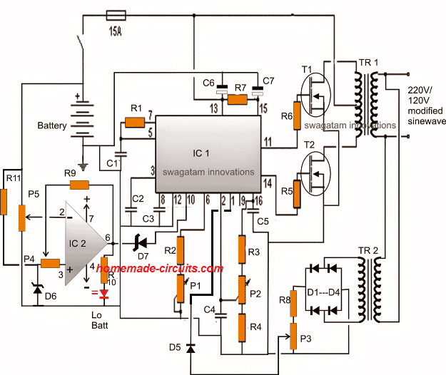
Here we can see that pin3 of the opamp now has it's own reference network using D6 and R11, and does not depend on the reference voltage from the IC 3525 pin16.
Pin6 of the opamp employs a zener diode in order to stop any leakages that might disturb pin10 of the SG3525 during its normal operations.
R11 = 10K
D6, D7 = zener diodes, 3.3V, 1/2 watt
Another Design with Automatic Output Feedback Correction
Circuit Design#2:
In the above section I have explained the basic version of IC SG3525 designed to produce a modified sine wave output when used in an inverter topology, and this basic design cannot be enhanced to produce a pure sine wave waveform in its typical format.
Although the modified squarewave or sine wave output could be OK with its RMS property and reasonably suitable for powering most electronic equipment, it can never match the quality of a pure sine wave inverter output.
Here I have explained a simple method which could be used for enhancing any standard SG3525 inverter circuit into a pure sine wave counterpart.
For the proposed enhancement the basic SG3525 inverter could be any standard SG3525 inverter design configured to produce an modified PWM output. This section is not crucial and any preferred variant could be selected (you can find plenty online with minor differences).
I have discussed a comprehensive article regarding how to convert a square wave inverter to a sine wave inverter in one of my earlier posts, here we apply the same principle for the upgrade.
How the Conversion from Squarewave to Sine wave Happens
You might be curious to know regarding what exactly happens in the process of the conversion which transforms the output into a pure sine wave suitable for all sensitive electronic loads.
It is basically done by optimizing the sharp rising and falling square wave pulses into a gently rising and falling waveform. This is executed by chopping or breaking the exiting square waves into number of uniform pieces.
In the actual sine wave, the waveform is created through an exponential rise and fall pattern where the sinusoidal wave gradually ascend and descend in the course of its cycles.
In the proposed idea, the waveform is not executed in an exponential, rather the square waves are chopped into pieces which ultimately takes the shape of a sine wave after some filtration.
The "chopping" is done by feeding a calculated PWM to the gates of the FET via a BJT buffer stage.
A typical circuit design for converting the SG3525 waveform into a pure sine wave waveform is shown below. This design is actually an universal design which may be implemented for upgrading all square wave inverters into sine wave inverters.
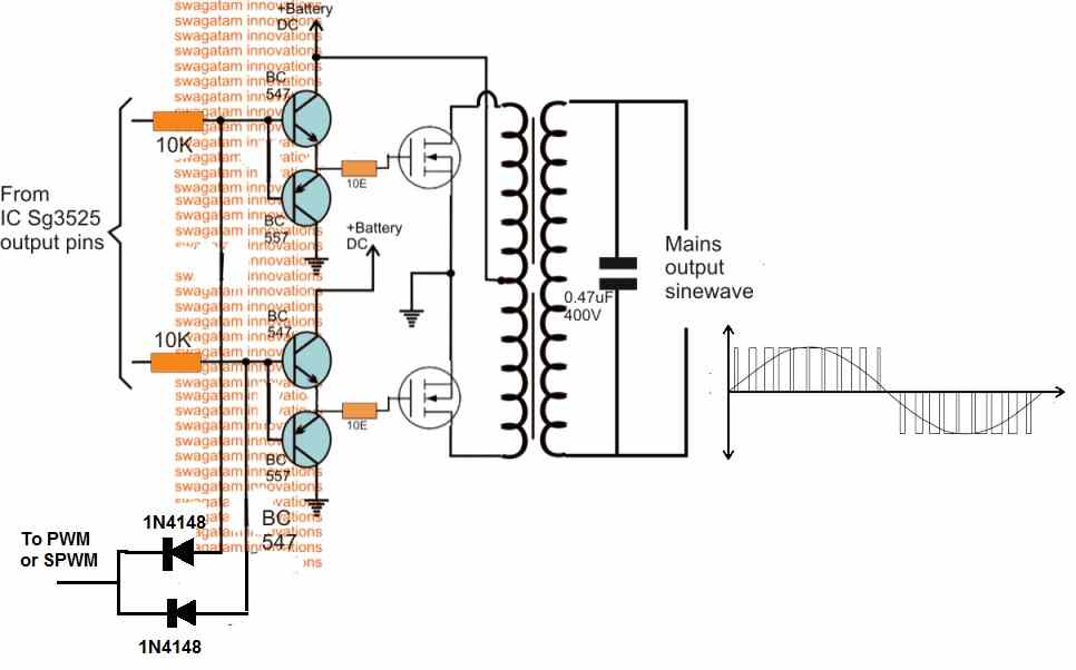
As may be in the above diagram, the lower two diodes are connected to a PWM feed or input, which causes the transistors to switch according to the PWM ON/OFF duty cycles.
This in turn rapidly chop the 50Hz pulses at the bases of the BC547/BC557 coming from the SG3525 output pins.
The above operation ultimately force the mosfets also to turn ON and OFF in the same pattern as the SPWM for each of the 50/60Hz cycles. This SPWM is then induced into the transformer primary by the MOSFETs, consequently producing a sine waveform at the output or the secondary side of the transformer.
If an ordinary PWM is used as I have explained below, then its frequency should be 4 times more than the base 50 or 60 Hz frequency. so that each 50/60Hz cycles are broken into 4 or 5 pieces and not more than this, which could otherwise give rise to unwanted harmonics and mosfet heating.
PWM Circuit
The PWM input feed for the above explained design can be acquired by using any standard IC 555 astable design as shown below:
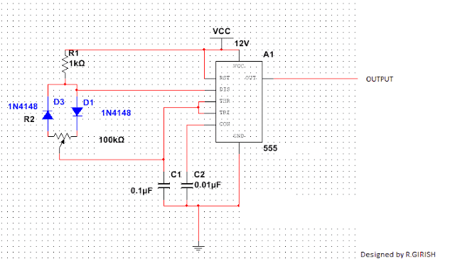
This IC 555 based PWM circuit can be used for feeding an optimized PWM to the bases of the BC547 transistors in the first design such that the output from the SG3525 inverter circuit acquires an RMS value close to mains pure sine wave waveform RMS value.
Using an SPWM
Although the above explained concept would greatly improve the square wave modified output of a typical SG3525 inverter circuit, an even better approach could be to go for an SPWM generator circuit.
In this concept the "chopping" of each of the square wave pulses is implemented through a proportionately varying PWM duty cycles rather than a fixed duty cycle.
I have already discussed how to generate SPWM using opamp, the same theory may be used for feeding the driver stage of any square wave inverter.
A simple circuit for generating SPWM can be seen below:
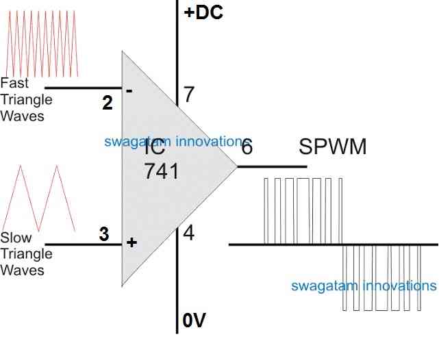
Using IC 741 for Processing SPWM
In this design we see a standard IC 741 opamp whose input pins are configured with a couple of triangle wave sources, one being much faster in frequency than the other.
The triangle waves could be manufactured from a standard IC 556 based circuit, wired as an astable and compactor, as shown below:
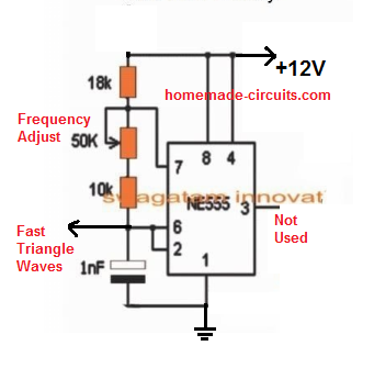
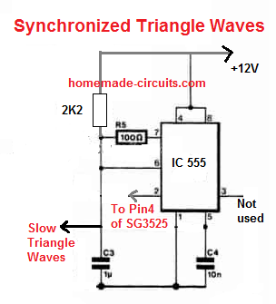
#UPDATE: The above "slow triangle waves" can be directly acquired from the Ct pin of the IC, that means you can now eliminate or ignore the above IC 555 stage for the slow triangle waves.
As can be seen in the above two images, the fast triangle waves are achieved from an ordinary IC 555 astable.
However, the slow triangle waves are acquired through an IC 555 wired like a "square wave to triangle wave generator".
The square waves or the rectangular waves are acquired from pin#4 of SG3525. This is important as it synchronizes the op amp 741 output perfectly with the 50 Hz frequency of the SG3525 circuit. This in turn creates correctly dimensioned SPWM sets across the two MOSFET channels.
When this optimized PWM is fed to the first circuit design causes the output from the transformer to produce a further improved and gentle sine waveform having properties much identical to a standard AC mains sine waveform.
However even for an SPWM, the RMS value will need to be correctly set initially in order to produce the correct voltage output at the output of the transformer.
Once implemented one can expect a real sine wave equivalent output from any SG3525 inverter design or may be from any square wave inverter model.
Finalized SG3525 Pure Sine Wave Inverter Circuit
The following diagram shows the finalized design of the pure sine wave inverter using IC SG3525 and SPWM, as per the above explanations.
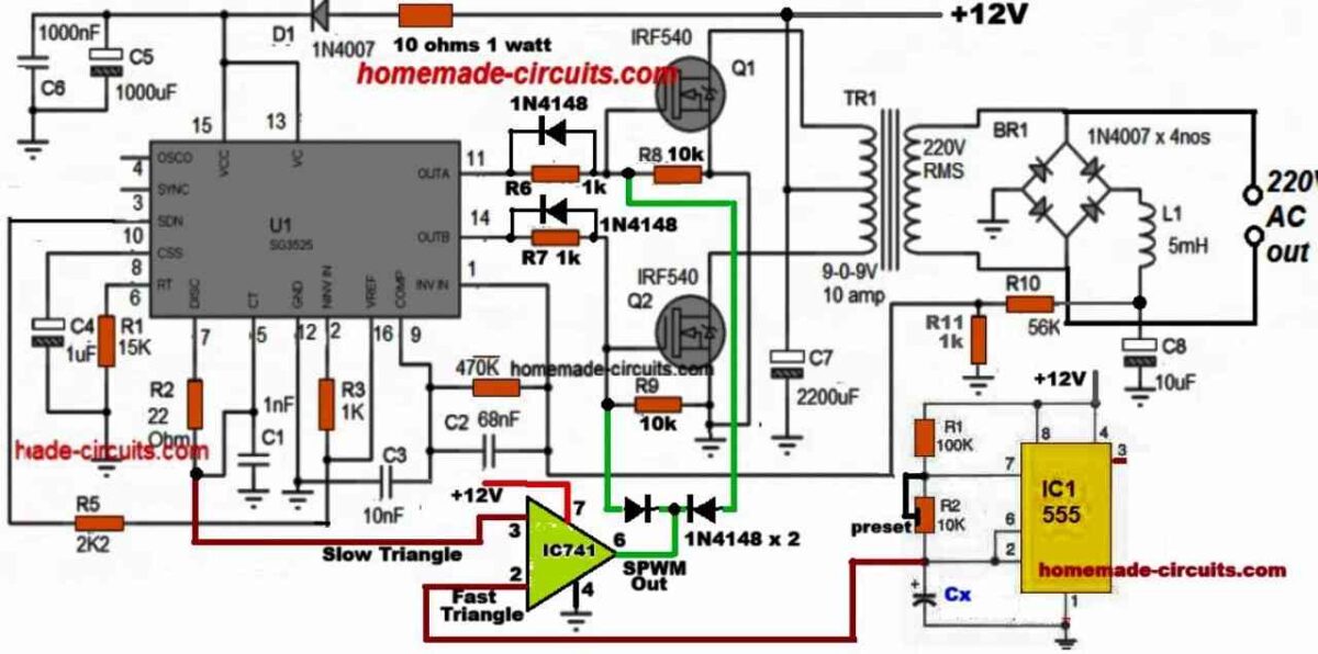
If you have any doubts regarding the above SG3525 pure sine wave inverter circuit you can feel free to express them through your comments.
UPDATE
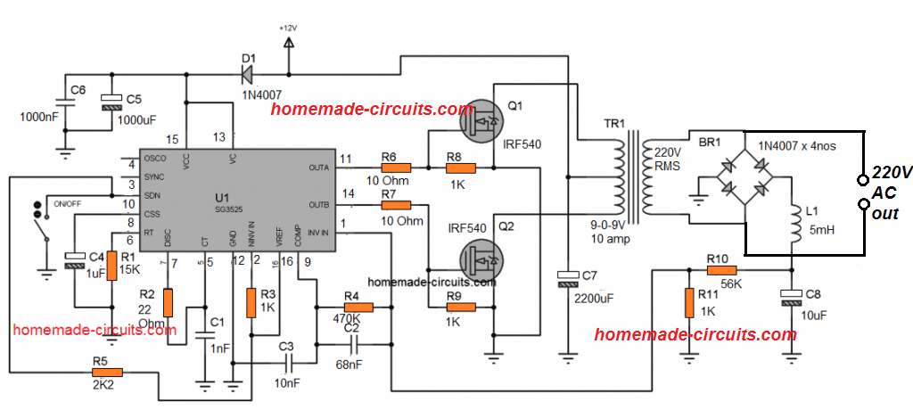
A basic example design of a SG3525 oscillator stage can be seen below, this design could be integrated with the above explained PWM sine wave BJT/mosfet stage for getting the required enhanced version of the SG3525 design:
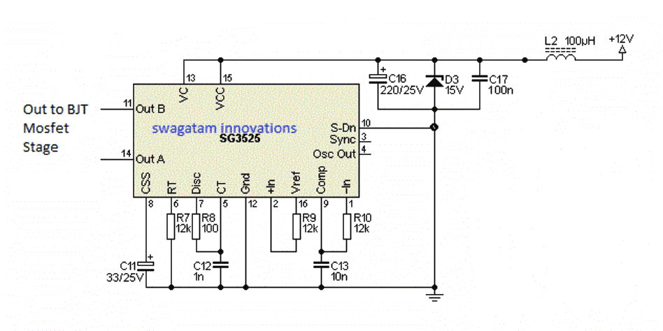
Complete circuit diagram and PCB layout for the proposed SG3525 pure sine wave inverter circuit.
Courtesy: Ainsworth Lynch
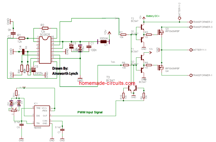
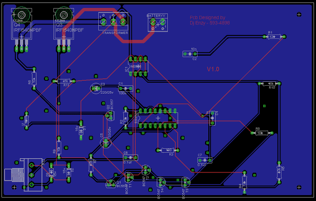
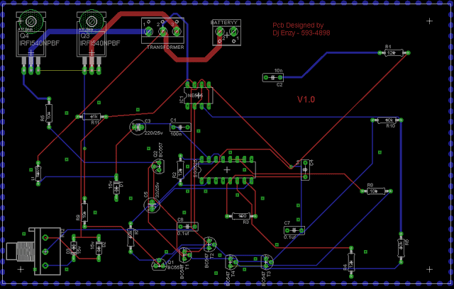
Design#3: 3kva Inverter circuit using the IC SG3525
In the previous paragraphs we have comprehensively discussed regarding how an SG3525 design could be converted into an efficient sine wave design, now let's discuss how a simple 2kva inverter circuit can be constructed using the IC SG3525, which can be easily upgraded to sine wave 10kva by increasing the battery, mosfet and the transformer specs.
The basic circuit is as per the design submitted by Mr. Anas Ahmad.
The explanation regarding the proposed SG3525 2kva inverter circuit can be understood from the following discussion:
hello swagatam, i constructed the following 3kva 24V inverter modified sine wave (i used 20 mosfet with resistor attached to each, moreover i used center tap transformer and i used SG3525 for oscillator).. now i want to convert it to pure sine wave, please how can i do that?
Basic Schematic
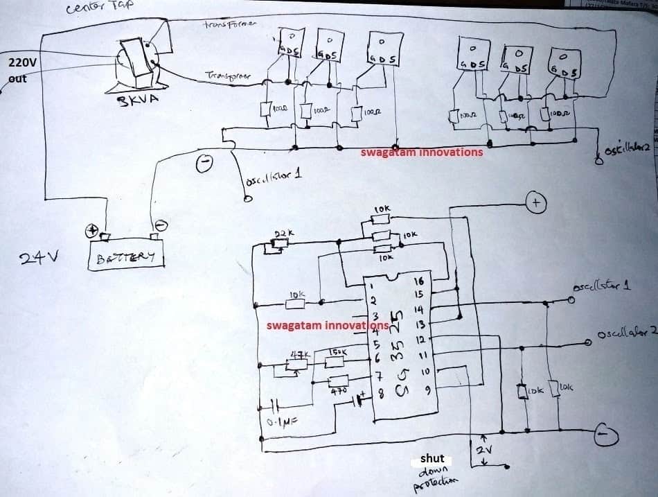
My Reply:
Hello Anas,
first try the basic set up as explained in this SG3525 inverter article, if everything goes well, after that you can try connecting more mosfets in parallel.....
the inverter shown in the above daigram is a basic square wave design, in order to convert it to sine wave you must follow the steps I have explained below The mosfet gate/resistor ends must be configured with a BJT stage and the 555 IC PWM should be connected as indicated in the following diagram:
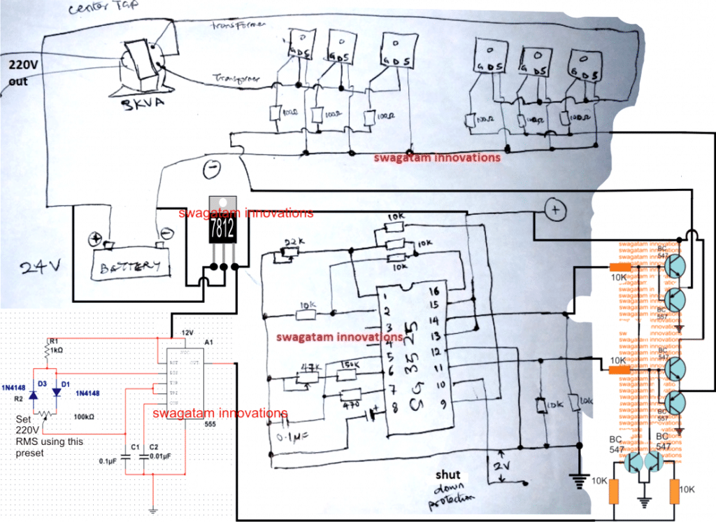
Regarding Connecting parallel mosfets
ok, i have 20 mosfet(10 on lead A, 10 on lead B), so i must attached 2 BJT to each mosfet, that's 40 BJT, and likewise i must connect only 2 BJT coming out from PWM in parallel to the 40 BJT? Sorry am novice just trying to pick up.
Answer:
No, each emitter junction of the respective BJT pair will hold 10 mosfets...therefore you will need only 4 BJTs in all....
Using BJTs as Buffers
1. ok if i may get you right, since you said 4 BJTs, 2 on lead A, 2 on lead B, THEN another 2 BJT from the output of PWM, right?
2. am using 24 volt battery hope no any modification to the BJT collector terminal to the battery?
3. i have to use variable resistor From oscillator to control the input voltage to the mosfet, but i don't know how i will go about the voltage that will go to the base of the BJT in this case, what will i do so that i want end up blow up the BJT?
Yes, NPN/PNP BJTs for the buffer stage, and two NPN with the PWM driver.
24V will not harm the BJT buffers, but make sure to use a 7812 for stepping it down to 12V for the SG3525 and the IC 555 stages.
You can use the IC 555 pot for adjusting the output voltage from the trafo and set it to 220V. remember your transformer must be rated lower than the battery voltage for getting optimum voltage at the output. if your battery is 24V you can use an 18-0-18V trafo.
Parts List
IC SG3525 Circuit
all resistors 1/4 watt 5% CFR unless otherwise specified
10K - 6nos
150K - 1no
470 ohm - 1no
presets 22K - 1no
preset 47K - 1no
Capacitors
0.1uF Ceramic - 1no
IC = SG3525
Mosfet/BJT Stage
All mosfets - IRF540 or any equivalent Gate resistors - 10 Ohms 1/4 watt (recommended)
All NPN BJTs are = BC547
All PNP BJTs are = BC557
Base Resistors are all 10K - 4nos
IC 555 PWM Stage
1K = 1no 100K pot - 1no
1N4148 Diode = 2nos
Capacitors 0.1uF Ceramic - 1no
10nF Ceramic - 1no
Miscellaneous IC 7812 - 1no
Battery - 12V 0r 24V 100AH Transformer as per specs.
A Simpler Alternative
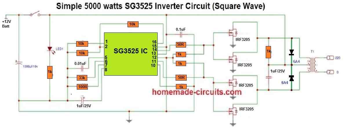

please I found out that the 18k resistor for the fast wave is getting very hot, I don’t know what went wrong/
There’s no way the 18k resistor should become hot? Even if you connect the 18k directly across the 12V DC supply still it cannot become hot?….how much DC supply are you using for powering the 555 and the SG3525 circuit?
I will try to update the complete schematic of the SG3525 sine wave inverter soon…
please before upgrading to spwm, the output frequency was 50Hz , but after it became 150hz, please assist
Please add a 3uF/400V PPC capacitor across the AC output of the transformer and check the frequency again, it should be 50Hz.
Hello sir, I noticed when I connect the spwm complete circuit, it works but after 10-15secs, it stops working. I restart again, same thing.
I now found out that the step down voltage regulator IC for 12v supply is getting hot when the spwm circuit was connected. but when I remove it, the regulator is not hot.
please kindly assist.
Hello Daniel, which schematic are you using exactly?
Good morning Sir
Thanks for the great work you are doing.
Sir I am interested in the last circuit. The 5000Watts square wave. And have two concerns
1) Can just those 4 MOSFETs 3205 be able to support 5000Watts?
2) please for the Circuit of a pure sine wave version of the 5000Watts Inverter.
thanks
Hello Ngang,
Sorry for the confusion, actually single 3205 MOSFETs cannot handle 5000 watts, especially when the voltage is 12v.
You would require at least 5 MOSFETs in parallel on each of the channels.
I would actually recommend IRFP2907 MOSFETs instead, which are even more powerful than 3205.
Okay Sir. Thanks very much for the clarification.
Sir, I need a 5000Watts pure sine wave inverter circuit diagram
Thank you NGANG, I think you can first complete the square wave 5000 watt inverter circuit and confirm the results then we can convert it to a sine wave inverter.
Sir, I made an inverter with 2 stages, my circuit was normal but for some reason an explosion occurred. now I’m fixing this circuit. stage 1 with sg3525 and stage 2 with egs002. My stage 2 is probably normal but for stage 1 it doesn’t seem like it. I did a load test after the transformer (before the stage 2 circuit) there was a drop in the power supply voltage/source voltage from 12v to 8v. I wonder, is my IC 3525 the problem or my HFT? inverter spec 1000watt 12v to 220 pure sine wave EE55 transformer
Hi Kwk,
I am not sure how a SG3525 can be used with EGS002? It is simply not required, because EGS002 by itself is a full-fledged inverter module and does not require any external oscillator IC? Let me know your opinion on this.
pls send me a full diagram of pure sine wave inverter with part label using sg352 4 or 4047ic
You can go through the following article, this may help you to learn the details:
https://www.homemade-circuits.com/designing-a-sine-wave-inverter-circuit-from-the-scratch-tutorial/
Hello sir, please I want to build an inverter with 60v input, please how I keep the battery well managed, not to have imbalance state. Thanks Engineer Swagatam
Hello Grace, If you are using many batteries in series, then you will need a balance charger circuit to keep proper balance across the batteries.
I have a balancer circuit, but it is not tested by me yet:
https://www.homemade-circuits.com/lipo-battery-balance-charger-circuit/
Hello Swagatam, I constructed the Basic modified sinewave inverter in design number one. But when i power the circuit the wires connected to the MOSFETS is burning out, I presume is because the current carrying capacity of the jumper wires are not good enough. So, I am changing the wires now to thicker once. My question is, without loading the circuit is the current flowing through the mosfet supposed to be that high to burn off the wires?
Hello Collins,
If your MOSFETs are burning that means there’s some serious fault in your circuit.
In that case please remove the MOSFETs and first confirm whether your IC outputs are generating the required frequency or not?
If you IC does not oscillate and produce the intended frequencies at the MOSFET gates then your MOSFETs and the transformer both might burn.
So, please disconnect the MOSFETs and confirm if the IC is oscillating or not.
Hello Swagatam,
Thank you for your response. I will do that and keep you posted.
No problem Collins, all the best to you.
Hello sir, will the Spwm generator link to in4148 or BC 547 for the bjt buffer stage, please which one is better?
Hello Daniel,
1N4148 is the better option, so please use iN4148 diodes for feeding the SPWM to the buffer BJT bases.
Thanks sir, please the direction of the diode will block current
Daniel, the diode direction is correct, it is supposed to be reverse biased…it is positioned to conduct during the off pulses from the the op amp output…
Is it in order in the article
Yes…
Hello Mr Swagatam, thank you for your informative lessons on electronics, it has been beneficial.
How can I synchronise Sg3525 IC to make 3-phase inverter?
Hello Seun,
I don’t think SG3525 ICs can be used to generate sequential 120 degree phase signals for operating MOSFETs in 3 phase configuration.
please sir, I need sg3524 inverter circuit with well controlled pin 9 to give constant output 220v AC irrespective the battery voltage. thanks
Daniel, the feedback can produce a constant voltage only as long as the battery voltage is above normal. If it drops below normal then the feedback cannot help.
Thanks, I agree with this, a colleague argues it remains constant, irrespective of the voltage
If the battery is low or if there’s an overload, the feedback cannot raise the voltage, the output voltage will drop. Please ask your colleague how to do it.
please how can I put a soft start to the inverter circuit
Capacitor at pin#8 of the SG3525 IC decides the soft start.
Thanks for your reply, I am working with Sg3524 IC, how will I add soft start, and value. Thanks.
For SG3524 IC soft start, connect a 1N4148 diode at pin#9, anode to pin#9, then connect its cathode to the positive of a 4.7uF capacitor, negative of the capacitor to ground.
Thanks Swagatam,I appreciate you. I already has 4.7uf and 1k resistor connected in series into pin 9 and ground. How should I add the diode then, sir?
Daniel, then i think you must replace the 1k with the diode, and check the response.
Thanks sir, how will I test it’s response.
2. if I want to incorporate your guide for Ana’s 3kva inverter using 555 timer only, will I adjust anything.
With the slow-start added, the output voltage will not rise quickly to 220V, rather after a second or two.
If you want to add soft-start to Ana’s circuit, you can do it by adding a capacitor between pin#8 and ground, no other changes would be required.
Sorry sir, I meant to make it pure sine wave for Anas circuit, is there anything, I will modify in the 555 timer. Thanks Swagatam.
For making a pure sine wave inverter, you will have to employ the opamp technique, using fast and slow triangle waves.
Hello sir, My breaker used to trip off when the MOSFET blows, but because My batteries a weaker, it doesn’t anymore, putting more stress on the battery.
Please can I get a trip off signal from the sg35xx IC to off the relay if I use relay instead of breaker. Thanks Swagatam.
Daniel, getting a trip off signal to turn OFF a relay may not possible, or may be complicated, however you can initiate an instant shut down of the inverter and prevent the MOSFFETs from blowing, by appropriately configuring the shut down feature of the IC.
hi swagatam
it seems 555 doesn’t provide perfect triangle instead provide sawtooth , is it not a problem?
second thing voltage level from ct pin of sg352x is lower than that from 555 pin2 (fast tringle ) lead opamp to not trigger
, using lm358 in place of ua741 is correct?
Hi Abu,
Yes, the triangle waves are not perfect but still we can get a reasonably good sine wave output. The sine output will be much better than a modified output. Actually the slow triangle wave must be a sine wave ideally.
What are the peak values of the two triangle waves, did you measure them, please specify if possible??
LM358 can be used, or a comparator IC can be also used with appropriate modifications.
peak voltage of slow triangle is about 5v and that of fast is about 11v
Even with this difference in peak voltage, spwm will be generated at the output of the opamp, because fast triangle waves would be comfortably intersecting the slow triangle waves.
Sir, from this comment, can I still 741 IC for processing the spwm, because Abu reported that there was no trigger from the slow and fast wave
Daniel, IC 741 can be used, please see my reply to Abu.
Thanks sir, you advised We use a Trafo 9-0-9 v, @ 9v the MOSFET blew but worked well without blowing @10v, can I still use the Trafo for the PSW
Daniel, At 9V the MOSFET should never blow, there could be some other hidden issues, for example mosfet not rated as per trafo current.
Hello sir, please why is the amperage readings from the clamp meter is confusing. When I plug the electric stove it reads 2.35amps and battery drains fast. But with other loads without the stove it reads 4.25amps but the battery last longer.
Hello Seun, I think your meter is malfunctioning, because it’s showing the wrong results.
Thanks for the reply. Please how can I make My inverter efficient so that the standby current consumption will be 0.95A like factory made inverter rather than 2.24Amps.
You can add an ON/OFF switch in series with the positive line which connects with the transformer. If the supply to the transformer or MOSFETs is switched OFF the standby current will reduce drastically.
Thanks for this advice, won’t the inverter be totally shut off, also, will the switch handle the current when it is on load, please kindly advise what to do to make it seamless
Only the load and the transformer would be switched OFF, the IC and the MOSFETs would remain operational and in a standby mode. You must use a switch that is appropriately rated, to handle the load cuurrent.
I put a circuit breaker as the switch but shut off the inverter. What is the difference between a switch and the breaker
There’s no difference unless your circuit breaker has an automatic turn OFF system.
I don’t understand automatic off, because it doesn’t trip off by itself. I put it off by myself.
In that case it is same as the switch, no difference.
To reduce the standby current from your inverter like that of the redimade ones, you need an inductor in series with the positive lead from the battery to the transformer centre tap (that is for push-pull configuration). Or you connect an inductor in series with one terminal of the transformer before it reaches the H-bridge MOSFET’s connection (that is for H-bridge configuration/ non center tap transformer).
The inductor must be wound on a ferrite ring core and big enough to handle the current require from the inverter also it should be 8turns to 12turns. Then the thickness of the wire must be specified with the current needed in the inverter.
Dear Mr. Swagatam,
If an inverter with 100 KW power output at 50 kHZ is to be built what core would you be using? Can you please specify a core?
Thanks and kind regards,
Job Thykkoottathil.
Hi Job,
For 50kHz only a ferrite core is suitable, so you can use a ferrite core transformer.
Dear Mr. Swagatam,
I was thinking of a ferrite core with permeability 1300G. But not sure what the effective area and other dimensions should be. Just wondered whether you could help.
Kind regards,
Job.
Dear Job,
I think you will have to calculate the parameters accurately. I have posted an article on this, you can refer to this for more info.
https://www.homemade-circuits.com/how-to-design-and-calculate-ferrite-core-transformers-for-inverters/
THANK YOU SO MUCH MR SWAGATAM FOR THE QUICK RESPONSE, I REALLY APPRECIATE.
You are welcome Godspower!
SIR, PLEASE CONVERTION TO SINE WAVE IN THE ABOVE CIRCUIT, WILL IT ALSO WORK FOR SG3524. THAT WHAT AM HAVING IN MY LOCATION NOW.
Yes, it will work for SG3524 also.
GOOD DAY MR SWAGATAM, PLEASE MY QUESTION IS TAKEN FROM THE CIRCUIT DIAGRAM OF MR ANAS, WHERE YOU REPLIED TO HIS CIRCUIT MY ADDING PWM AND THE BJT TO CHOP THE SIGNAL FROM PIN 11 AND 14.
Hi Godspower,
If the voltage to the ICs are regulated using a 7812 ic, or a 7809 ic then the pwm will be stable, and the output voltage will also be stable and there won’t be any need of using a feed back.
The 741 ic circuit is universal.
Hi. I am reading this article very closely and I am confused with circuit design #1 wherein a small sensing transformer TR2 is used. The article states that the rectified output of TR2 is fed to Pin 2 (non-inverting input) of the SG3525S IC. However, looking at the circuit schematic, it seems that this rectified output is actually fed to Pin 1 (inverting input). Can you please clarify. Thank you very much.
Hi,
Sorry for the confusion. Yes, the feedback from the sensing transformer goes to Pin#1 and not Pin#2. Pin#2 is the reference pinout clamped with 5.1V reference value. I have corrected the typo accordingly now.
Hi, Mr. Swagatam, I had been following you r articles here in the Philippines. If I may, can you send me a complete detailed drawing for the PSW circuit you designed and inserted/incorporated to the basic 5kva 24vdc 220v output inverter by Mr. ANAS HAMAS.. Can you help me to have a PCB layout of that 5kva PSW inverter circuit? I am not a professional tech but only a newbie but can follow instructions.
Thank you for this opportunity to connect with you.
Egay Diolola
Thank you Edgardo, glad to meet you.
I understand you want to build the 5kva PSW inverter, however designing the PCB can be extremely time consuming so it won’t be possible for me to provide the PCB design.
That said, you should not build the whole 5kva circuit at once, you must first build a basic 100 watt version, then integrate the sine PWM and check the results, if everything works correctly, only then you must upgrade the MOSFFETs and the transformer for building the 5kva version.
Also, this design is very complex and will require testing and confirming the stages through an oscilloscope, therefore it may not be recommended for any newcomer, please proceed with caution.
Pls if we can get a pure sine wave using the ic sg3525 used above, i will also be happy because i undertand the schematics above more. I’m new to this, please be simple in explanations, i will appreciate that so much sir. thanks, waiting for yor reply.
Hi, In the above article I have explained elaborately regarding how to implement the pure sine wave feature in a SG3525 inverter circuit. You will read it carefully to understand all the steps.
Thank you very much, I appreciate this response and how fast it came through.
Hello,
First, I want to say thanks for your sharing of this knowledge of yours in this simple way, though not all that simple for me. my question is that I’m working on a pure sine wave inverter and I’m working with a cd4047, can you help me witth a more suitable schematics or guide on that, i have been seeing people working with CD4047 but they always have theri oscillator pin 13 left out, they don’t seem to have the explanations on why they did that, leaving the pin empty. I’m expecting your reply sir, thanks again.
For a 4047 pure sine wave inverter you can refer to the following post:
https://www.homemade-circuits.com/pure-sine-wave-inverter-circuit-using/
Regarding the output pinouts suppose your 4047 IC is set to produce 50 Hz frequency, then the pin#10 and pin#11 will alternately generate 50 Hz frequency while the pin#13 will generate a 100 Hz frequency.
Ok, thanks.
Bonjour chers techniciens merci pour cette matière
You are welcome Richard!
Is it necessary to include the error voltage circuit powered by 0-12volts transformer through the 2.2K pot as part in the Pure Sinewave Inverter Circuit, OR it’s unnecessary?
I am unable to find any circuit with 2.2K pot, please given more details about which circuit design you are referring to?
Hello. About the Pure Sinewave Inverter Circuit, should I use two 15v zener diodes or two 1N 4148 in the PWM circuit?
Secondly, what should I incorporate/consider as most important circuit, Short circuit/overload current protection OR Low battery & overload protection?
Hello, You will have to use 1N4148 diodes as shown in the diagram.
All those can be considered important. For the protections you may incorporate suitable feedback networks, as explained in the following article:
https://www.homemade-circuits.com/inverter-circuit-with-feedback-control/
I need circuit idea for High frequency plastic welding (dielectric heating)
old circuit all are using vacuum tubes such like 833a. 7t85 rb.7t69rb
but I need igbt based circuit
out put capacity is 5kw frequency 27mhz
Sorry, I do not have this circuit with me right now.
Can use sg3524 circuit to replace the sg3525 circuit
Yes you can do it.
Can I use this circuit to power twenty mosfets
Sure, you can put as many MOSFETs as you want.
Hello Sir Swagatam!
Hello Laszlo!
Thank You! Commenten My Easun Inverter pure sine 3000 w distroed modul ,diy replacement
Sorry, an exact DIY replacement module may not be possible for your specific inverter, you will have to contact the manufacturer for the module board.
Hello, sir,
Is there an error in the last diagram “A simpler alternative”? the resistor connected to the seventh leg goes to minus, but should go from the 7th leg to the resistor and to the 5th leg of the microcircuit;
Thank you
Hello Danil, You are absolutely correct, thank you! I have added the correction message just under the image.
Hello sir,
Can I use BD139/BD140 in place of BC547/BC557.
Thanks
Hello Olusegun,
Yes, you can use them, but that will be unnecessarily costlier and bulkier.
Thanks for your quick response all the time. I have them at my disposal. That’s why I’m asking.
No problem! You can use them.
Sir, can I get a pure sine wave non transformer based inverter circuit diagram
Hi George, you can refer to the following article:
https://www.homemade-circuits.com/5kva-transformerless-inverter-circuit/
What is the difference between 4MOSFET and 6 MOSFET amps or volt gain please replay ,can I change 4 MOSFET board instead of 6 MOSFET board in bus mini inverter
If you increase the number of MOSFETs in parallel it will increase the power handling capacity of your inverter and vice versa. How many MOSFETs to be used in parallel will depend on the max power requirement of the load.
Dear Swagatam
I first wanted to build the 50hz modified sine wave inverter before converting it to pure sine with the sg3525 I, my problem now is that all 6 pcs of the sg 3525 ic are fake so I have no alternative other than to use the tl494, I have successfully built one as described in your blog but I am getting a frequency of 400hz and above, any help please for 50 hz
Hi Richard,
Unfortunately the frequency of a TL494 IC cannot be reduced to 50 Hz, so we cannot do anything about it. You can instead try a 4017 IC based modified inverter circuit with perfection and with a 50 Hz frequency.
I have made this project and it works well but I have made some changes to it which enable me to get the true pure sine wave at the output .
The changes are:
1: for my external fast PWM generator that I use to breakdown the slow PWM from SG3525 circuit I used 50% duty circles mark 555time circuit.
2: I set the frequency of the fast PWM generator to 16khz which enables the multiple breakdowns of the 50hz that is generating from the SG3525 circuit.
With this configuration it gives me a true pure sine wave at the output after applying 1uf/450v capacitor.
The value of the capacitor is chosen in respect to the capacity of the inverter, my inverter capacity is 1kva which is 850w so one can select the value of the capacitor due to it inverter capacity for 1.5kva one can use 1.2uf/450 to 1.5uf/450v, for 3.7kva is 2.5uf/450v, for 500va is 0.22uf/400v to 0.47uf/400v, for 5kva is 4.75uf/450v, and etc.
Thank you so much Emmanuel, for your valuable suggestions. Glad you could build the sine wave version successfully.
I appreciate it very much. I hope the readers will find it very useful.
You are welcome swagatam and I also appreciate your love in sharing your knowledge to people who are willing to learn.
Another thing I will say is that please you should always verify any circuit you upload and see their performance before uploading, the reason I’m saying this is that there is no workable 50Hz inverter circuit in this article here and I have gone through comments and I have seen people complaining about heating of MOSFET and different types of malfunction of their circuit, the reason is because non of the circuit that I have seen here is 50Hz because they are high frequency circuits (50khz) not low frequency circuit(50hz). If you want them to work at 50hz then the capacitor at Ct pin of the SG3525 should be 0.1uf not 1nf, and the resistance at Rt pin of the SG3525 should be 142400 ohms (142k4) not 15000 ohms (15k) and resistance at Rd pin should be 100 ohms (100R), with this configuration one can achieve 50hz at the output of the transformer and another thing is oscillating output pin of the SG3525 which is pin4 should not be tempered with because it will distorted the output pulse of pin14 and pin11 of SG3525.
With all of the explanations I think everyone should be able to set up his system and I will surges anyone trying to design this project should first try and design the PWM version and see whether is working fine before going for this SPWM version.
Thanks for having me.
Hi Emmanuel, I appreciate your suggestion, however it is not possible to check and test each and every circuit before uploading. Moreover these types of circuits are meant for people who are well versed with electronics and basically know how to fix small issues in a circuit, just as you did. The design of the concept is the crucial thing which must be perfectly examined before posting, and I always do that.
Anyway, thanks again for your valuable inputs, I am sure other visitors will benefit a lot from them.
You are welcome sir
thanks for accepting my opinion.
please sir, can you simplify how he got 50% duty cycle with 555 timer.. thanks Swagatam
Daniel, the 50% duty cycle can be adjusted by correctly calculating the timing components of the 555 astable circuit, although it can never be a perfect 50%
please sir, do you recommend I configure the fast generator wave from 555 circuit above to 16khz as it was done by Emmanuel and pick slow wave directly from CT pin 7 of sg3524ic, or I do the 555 timer circuit for slow wave. thanks
Daniel,
You can pick the slow triangle waves from Ct pin of the IC, that’s crucial. And the fast triangle waves can be from any suitable source.
The fast triangle wave frequency can be any value, right from 400 Hz to 100 kHz, however if it is higher than 500 Hz then the transformer will need to be a ferrite core transformer.
can’t I use laminated transformer at all, I see some psw inverter using it
You can use it, but then the spwm frequency cannot be higher than 400 Hz…
Sir, from Emmanuel design, he used 16khz, then how will I compensate with using around 400hz and 50hz slow wave to give a pure sine wave.
Use 400Hz for the fast triangle waves instead of 16kHz
in my pure sine wave inverter design I used the fast PWM generator to the base of BC547 design not SPWM generator to the base of BC547 design.
that why I chose the fast frequency to be 16khz, reason is the higher the frequency from the fast PWM generator to the base of the BC547 transistor that drives the MOSFETS, the cleaner the sine waves will be at the end of the transformer after filtering with capacitor
Thanks Swatagam and Emmanuel for all your inputs, how did you set 50 d.c and 16khz on 555 timer for the fast wave generator. can I get both values with the fast wave circuit above.
Daniel,
You can use any online “555 astable calculator software” to calculate the resistor and capacitor values for getting 16 kHz frequency and 50% duty cycle….
Thanks sir, Will the fast wave output be picked from pin 2/6 or pin 3 to bc547
pin2/6, The details are already given in the above article, you can check it.
There’s no BC547. It will go to an opamp.
you are welcome ? Daniel.
for the 50% d.c. I used different designs. it just that I have knowledge in electronics circuit design and what I did was getting to know on how to design a pure sine waves inverter here in this site and i went to design my own pure sine wave inverter.
so you can get the 50% d.c. PWM generator circuit online by search for 50% mark-space ratio Astable Multivibrator circuit on Google then you will find it there and for getting the required frequency you need to calculate it with the use of this formula (0.72÷(R×C)) or you can choose the capacitor C to be 0.1uf which is 104 then input the required frequency in place of resistor R in the formula e.g (0.72÷((0.1×10^-6)(16000))) which the required resistance is 450 ohms, then you will make use of 1 kilohms veritable resistor to set the resistance to 450 ohms. With this method you will be able to generate 16khz PWM with 50% mark-space ratio.
Do I need a snubber circuit for the inverter? What is the function?
hello Emmanuel, can I get in touch with you , I need some clarification .if u don’t mind
Please Sirs, can I use 6v-0-6v transformer to generate pure sine wave inverter? Or what is the best recommended transformer voltage?
Please why is 12v-0-12v is not used?
Daniel,
The transformer voltage must be in line with the SPWM average DC voltage or the switching voltage of the transistors.
If the battery is 12V the SPWM chops is to an average level of 6V or 7V, that is why the transformer primary must be also rated at this level. If you use a 12V transformer with a 6V SPWM, the output voltage from the transformer will turn into 110V and not 220V.
Thanks Swagatam, I appreciate your response. At 12v full battery 14v will the output voltage be 220v at 6v
At 14V the output should be 250V, however after full charging the battery voltage will drop to 12.6V from 14V.
Yes sir swagatam i tried almost 90 percent of your circuit they’re working but
I do not trust any circuit without your name (swagatam innovation ) thankyou
Thank you for your kind feedback Hamisu. You could build the circuits because you understood them well before trying, and you could troubleshoot any small mistakes the circuit might have had.
How can I connect pin10 of sg3525 to cutoff when battery is low
It is already shown in the first two diagrams. See pin#10 connections.
Thanks for this lesson. But have these questions to assist my project:
1. How do I build a strong sign wave (PWM) oscillator, with SG3525 IC, capable of driving a 4000watt inverter mosfet stage?
2. How do I determine the capacity of solar panels to charge the batteries?
The power of the inverter has nothing to do with PWM oscillator frequency, it solely depends on the power capacity of the transformer, battery and the mosfets
The solar panel must be able to deliver a voltage equal to the full charge level of the battery and a current that is at least 20% of the battery’s Ah value.
Hello sir my self raghavendra from karnataka I am follower of your web site and all the circuit that you have provided are working fine without any problem thanks for , but sir I have made the inverter refering to your diagram using ic sg3525 sir it’s working but it’s one of the mosfet is getting much hotter so please do provided the solution
Thank you Raghavendra. MOSFETs are sensitive unpredictable items which can burn due to many reasons. You can change the mosfet and check whether the new mosfet also heats up or not. Additionally you can include some mosfet protections as explained in the following article
How to Protect MOSFETs – Basics Explained
Alternatively you can replace the mosfet with 2N3055 transistor configured in Darlington mode with 2N2222 transistor
BJTs are more reliable than mosfets and do not burn easily unless configured incorrectly.
Thanks for your valuable reply sir, even when I new mosfet the result is same sir so
As you would know that both the output pins of SG3525 generate identical frequencies, so it is difficult to judge why one mosfet is getting hotter.
You can try putting a reverse diode across drain/source of the mosfet and also a diode across the gate resistor. Additionally put a 1K resistor across gate/source of the mosfets.
I really appreciate this circuit. Many thanks for sharing this. I have a doubt about the ways to synchronize high frecuncy used to produce the SPWM with the PWM (low frequency) with the aim of producing a synchronized SPWM that can divide the low PWM.
From this circuit I can not see the link to the SG3525 oscilator to produce a synchronized 400 hz.
About the section that says “upgrade” the pin 4 (OSC) of SG3525 produces the double of frecuency respect the output (because an internal flip flop of the IC).
I really appreciate your calrification please.
Thank you for the question! According to my understanding pin#4 should produce a waveform that will correspond to each cycle generating from pin#11 and pin#14 of the IC. And these waveform when applied to the 555 IC will transform them into corresponding triangle waves which will again correspond to each waveform cycle generating across the outputs pin#11 and 14 of the IC. In this way the SPWM will be perfectly synchronized with the output waveform of the IC.
The other alternative is to take the synchronized triangle wave directly from the Ct pinout of the IC and use it as the slow triangle wave for the Op amp.
Many thanks for your quick response. This seems very good idea and I will try it as soon.
Sure, no problem. All the best to you!
Sir. I build the circuit using KA3525, I have taken feedback and given to pin 1. At no load it s working fine. If i connect load the output voltage drops, to 10 to 15V , same is reflected in feedback voltage as well, but duty cycle not increased to match the voltage drop. For any type of load the duty cycle remains same. Can u help me to solve. I used 500VA Transformer sir.
Gurusivakumar, what are the battery, transformer, load specifications? did you check the voltage without the feedback setup?
Please check the output voltage without the feedback and with load connected.
If still the voltage drops then the problem could be over-current or insufficient battery/transformer current compared to load current
I used DC Regulated power supply. For me the IC gives output pulses even the feedback are not present. Feedback does not affect PWM pulses. I checked with no load the voltage is 220V. Am not applying heavy load. i am just applying load say 18W CFL bulb, and the voltage becomes 205V. I am unable to get why my PWM is not varied when the voltage drops? It is supposed to increase the duty cycle . Whether it is transformer winding losses? I am getting voltage drop in primary side of transformer as well.
If it is due to over load then the feedback and PWM will not help. DC regulated power supply will not work. You must use a battery. If it is a power supply then make sure it is able to supply at least 3 amp to 5 amps and the transformer is also rated at 3 amp or 5 amp to handle a 18 watt lamp.
Sir, my Regulated DC power supply is rated 10A and Transformer is rated 2A in 230v Side. So i am sure it is not an overload issue when i connect a 15W load.
It looks like a transformer problem then, because a 2 amp means it could be 1.5 amp in reality, along with losses it could be just 1 amp. If the voltage is dropping without feedback and PWM issue then the problem is surely associated with either the power supply or the transformer.
Try a different transformer and check the results.
Sure sir. I will check and Update. Thanks for your replies.
Sir at that BJT stage am getting 1.49 volt at that 10 ohms resistor is it suitable for driving the mosfet gate please tell me what could be the problem.
Jonh, you must get at least 50% of the supply voltage, 1.49 is not correct or maybe you are doing something wrong.
sir is SG3525 a square wave inverter or modified sine wave
It is a square wave inverter which can be converted into a modified sinewave through PWM adjustment.
sir please if i use two irfp260n One on each channel with 9v 20amp transformer how many watts will i get
You will get 9 x 20 = 180 watts. Mosfet is only for switching the battery/transformer current, it itself cannot generate power.
sir between irfp260 and irf3205 which one is more perfect
John, It depends on the application specifications. If the inverter spec is less than 40 V then IRF3205 is good, otherwise IRFP260 is suitable.
sir please between bread board and Vero board which one is more good for assembling this components
I always use veroboard and assemble by soldering the components, which gives confirmed results.
Sir
I am interested in building a two stage 12V DC (car battery) to HV DC to 240v AC 50 Hz output 2KW inverter utilising the pure sine wave module EGS002 in a configuration utilising HF ferrite transformers to generate the boost voltage. I can see that a solution is given showing a 400V DC mosfet rail in the EGS002 datasheet but how to implement the 400V DC rail?. I assume a multi mosfet arrangement with associated bootstrap drivers switching the DC through a ferrite transformer will be necessary and then rectify and smooth through some high voltage and current diodes to achieve the required drain and source DC voltage for switching from the EGS002. I am not sure how to calculate what transformer I should use. Your wisdom in such matters exceeds mine, so do you have any thoughts please relating to the EGS002 in this two stage configuration please and transformer type to use?
Many thanks
Steve
Steve,
Calculating a ferrite transformer is a long and tedious process which you will have to do yourself with lot of patience, and then test it practically. I have a related post which explains in details how to do it.
https://www.homemade-circuits.com/how-to-design-and-calculate-ferrite-core-transformers-for-inverters/
You can try a basic design first and check whether it is working with the EGS002 module or not. If it works then you can upgrade the mosfets and the transformer accordingly.
sir if i want to use that Ainsworth Lynch SG3525 oscillation stage diagram without spwm and the BJT stage should I connect the output pin of SG directly to the mosfet or should attached 1k resistor from gate to source.
You can do it as done in the following diagram:
https://www.homemade-circuits.com/wp-content/uploads/2019/04/feedback-1024×460.png
sir you are right there was a mistake in my connection for that Ainsworth Lynch diagram. i have correct it and now it’s working but it is giving output of 30v I don’t know if the problem is from the ic or my mosfet is burnt
sir the Ainsworth Lynch diagram is working but the transformer out put is showing 30vac please what could be the issue
John, That means your transformer wires are not connected correctly. If you are using a 12V battery then you must use a 9-0-9V transformer.
Sir am referring to Ainsworth Lynch SG3525 oscillation stage.
What issues are you facing?
I built the SG3525 oscillation stage but it is not working
All the above SG3525 circuits will work, and has been tested by many people. There may be some problem with your IC or the connections.
Try with this circuit again:
https://www.homemade-circuits.com/wp-content/uploads/2019/04/feedback-1024×460.png
sir is UA 741 the same thing with lm 741
Yes both are one and the same…
sir please are you on Facebook or WhatsApp please tell me your name i want to show you one of your circuit diagram that I built but it is not working.
John, please post the link of the diagram that you are referring to, I will explain the mistakes you might have made while building it.
I will discus it here through comments.