In this post I will comprehensively explain 3 easy to build 10 watt power amplifier circuits, which can be built using discrete parts, such as resistors, transistors, and MOSFETs. The MOSFETs used in these designs are the ordinary IRF540 and IRF9540, that are easily avail;able in the market and are quite inexpensive.
True Complementary 10 Watt Amplifier Circuit
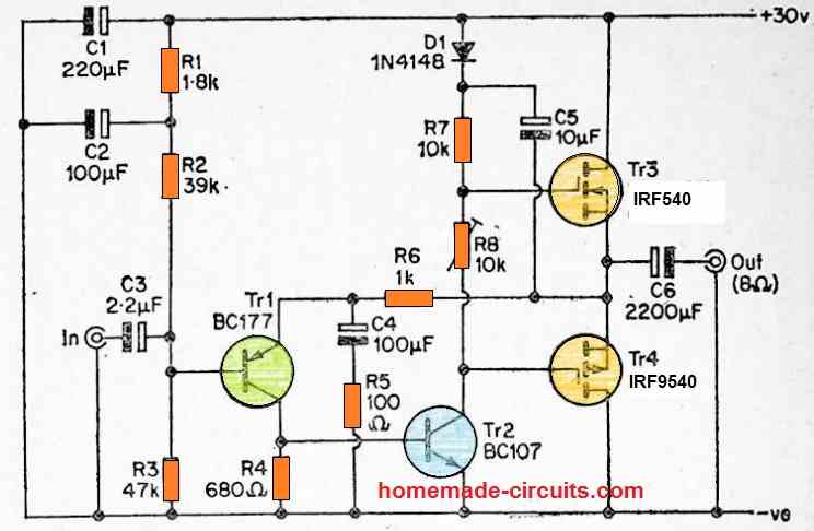
The first design in Figure 1 below depicts the circuit design of a basic, true complementary 10 watt MOSFET amplifier.
This is a well-known configuration in which a common emitter input stage (Tr1) drives a common emitter driver stage directly (Tr2).
This, subsequently, operates a couple of complementary emitter follower output transistors, or complementary source follower output transistors in this case.
Feedback Biasing
Due to the feedback supplied by R6 through the amplifier output (Tr3 and Tr4 sources) to the emitter of Tr1, there is almost 100 percent negative feedback at DC.
This enables the output biasing to be simple, and to approximately half the supply potential, since all that is required is to use a resistive divider to bias the input (Tr1's base) to this level.
R1, R2, R3, and C2 constitute the bias circuit. R1 and C2 filter out whatever hum or noise that would otherwise flow through the supply lines to the amplifier's input via the bias network.
Normally, the output voltage swing (and therefore the power) would be biased to 1/2 the supply voltage to avoid clipping and significant distortion.
As we'll see in a moment, the best results in this situation come from a little bigger quiescent output voltage, so that the circuit is biased appropriately.
R4 is Tr1's collector load, and it has a value of around 1mA, which keeps Tr1's collector current at a reasonable level. Tr2's main collector load is R7, and R8 is also included in Tr2's collector load.
The R8 adjusts the quiescent bias current via the output transistors, and is set to draw an overall quiescent current of around 30mA.
Although it would be normal to use a transistor or diodes for the bias circuit to enable temperature compensation if bipolar devices had been used for the output transistors.
This is not necessary with here, because the two output MOSFETs have a negative temperature coefficient and therefore will end up causing a small decrease in the quiescent output current once they overheat while operating .
There is therefore no danger of thermal runaway, and there is no requirement for temperature control, because the little reduction in output bias current that occurs while the output MOSFETs heat up has no tangible effect.
MOSFETs vs BJTs
When compared to bipolar devices in an analogous circuit, one drawback of MOSFETs employed in this sort of design is their reduced efficiency.
The input voltage at the base of the transistor causes a roughly equal variation in the output voltage at the emitter when utilized in the emitter follower configuration, and the voltage drop between the base and emitter pins of a BJT is only approximately 0.65 volts.
The voltage gain isn't exactly unity, but it's usually about 0.98, which is acceptable enough for high efficiency in a circuit such as this, with an output voltage swing that's not too far from the supply voltage level when the amplifier is fully powered.
A MOSFET device, unlike a BJT, is specified with a gate threshold voltage which is somewhat higher than the corresponding voltage in a BJT device, resulting in a reduced output voltage shift.
That said, with bipolar power amplifiers, it is common to employ a Darlington pair or other similar configuration for each output device, thereby causing the base threshold voltage to become two times more.
However, MOSFET devices can still exhibit lower efficiency since they require a large gate to source voltage to bias them strongly into conduction, while a bipolar device requires only a slightly greater base to emitter voltage than its base threshold voltage to attain an equivalent degree of conduction.
When employed in the source follower mode, a MOSFET device delivers significantly less than unity voltage gain, and the voltage drop across the gate to source turns more high as the output current rises.
Using Bootstrapping
The bootstrapping approach is one method of reducing this issue, and C5 and D1 offer the bootstrapping in this architecture.
D1 allows current to flow via R7, R8, and Tr2 when the circuit is idle, consequently it has minimal influence on the circuit. C5 links the increment in voltage to the junction of D1 and R7 as soon as the output goes positive.
Hence, The supply voltage to the driver stage is perfectly increased through a value equivalent to the change in output voltage on positive going output signals (minus the D1's voltage drop of around 0.5 V).
The bootstrapping signal should be isolated from the positive supply voltage, therefore D1 must be added.
A resistor in the D1 place is rather standard in this type of circuit (that is also used widely in bipolar designs to enhance the output power).
However if a resistor is used for D1 then the C5 capacitor would have face a lower impedance and will need to be a larger value capacitor in order to guarantee better performance at lower frequencies.
The idea of including the bootstrapping network is that it allows Tr3 to get a gate voltage that is greater than the positive supply voltage.
Because of this even with a voltage drop of many volts between its gate and source terminals, it is able to produce a source potential which is almost equivalent to the positive rail voltage.
One disadvantage of the bootstrapping approach is that it only produces the intended impact across one set of half cycles, in this instance the positive going half cycles.
Because the collector voltage of Tr2 cannot exactly slide down to the negative supply voltage, the minimum driving voltage accessible to Tr4 remains 0V, or a bit higher in fact.
With a lowest gate voltage of slightly over 0V, Tr4's lowest source voltage under high output current situations must be many volts lower than this gate voltage.
To compensate for this, a little higher supply voltage than would typically be used for an amplifier with this power rating and load impedance must be used.
As previously stated, the output is biased to somewhat higher than half of the supply voltage, which is required since the output would otherwise clip on negative peaks long before clipping of positive output peaks.
Biasing the output with a few volts more than half the source voltage guarantees almost symmetrical clipping and the highest output power for a given supply voltage.
Efficiency and Gain
With the stated settings, the amplifier's voltage gain is roughly equivalent to R6 divided by R5, or around 10 times (20dB). However, by altering the value of R5, the circuit's voltage gain may be adjusted to meet specific needs within reason. Just like with any audio amplifier layout, efficiency might differ slightly from one sample to the next.
Nevertheless, the design's distortion level appears to be equivalent to that of basic BJT circuits, with an effective harmonic distortion of lower than 0.1 percent at all input power ranges.
The circuit's open loop gain (i.e. the voltage in the absence of a negative feedback) is almost constant across the full audio frequency spectrum, thus there should be little drop at increasing audio frequencies.
The absence of any parts in this design to enable high frequency roll-off or phase correction might surprise readers who are accustomed with BJT systems of this sort.
Power Output
When utilizing a 30 volt (loaded) supply, the circuit's output power is generally around 6 to 7 watts RMS into an 8 ohm loudspeaker.
A supply of around 36 volts may produce a greater output power of approximately around 10 watts RMS, which is roughly the highest loaded supply voltage that must not be exceeded.
It's worth noting that the output devices (particularly Tr4) generate a lot of heat, thus they need to be installed on big heatsinks.
10 Watt Amplifier using Quasi Complementary MOSFET Stage
A reasonably good 10 watt RMS amplifier employing a quasi complementary, Class B MOSFET output stage is shown in Figure 2.
With a positive going output, a source follower transistor (Tr3) works to drive the load, and bootstrapping (supplied by D1 and C6) is utilized to deliver superior efficiency on positive going outputs, as in earlier designs.
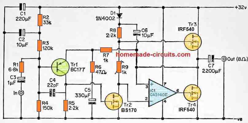
During the time the output is negative going, the load is powered by Tr3 in common source mode, which, like the earlier circuit, provides good performance on negative going outputs.
Tr3 is accompanied by an operational amplifier whose non-inverting input is linked to the amplifier's output (Tr3 and Tr4 sources). Given that the signal is reversed via Tr4, this results in 100% negative feedback between Tr4 and 1C1.
This results in unity voltage gain from 1C1's inverting input to the amplifier's output, resulting in a fairly decent match to Tr3.
There is a little discrepancy since Tr4 and 1C1 yield almost precise unity, but the voltage gain of Tr3 (as previously described) will be substantially lower than unity.
However, because the circuit features a significant amount of general negative feedback to balance out the mismatch and assure minimum distortion levels, this is of little actual significance. 1C1 is a kind with a PMOS input stage, and as a result, it has a very high input impedance, equivalent to a MOSFET device.
Adjusting the Quiescent Current
The driver stage employs a MOSFET in common source mode (Tr2), with R9 serving as the primary collector load and R10 providing the necessary quiescent bias current to the output transistors.
To avoid a large bias current across the output transistors (and the potential of harming these transistors as a result), R10 should be adjusted to nearly zero resistance at first. R10 may be subsequently tweaked for increasing resistance until the amplifier draws around 30mA of current.
Tr1 serves as the common emitter input stage, which is tied directly to Tr2, with R6 serving as the Tr1 collector load.
Despite the circuits using a bipolar driver stage in this basic design can work without using a load resistor for the input stage (the driver transistor's base-emitter junction provides a high but workable resistance), the resistor has to be used in this circuit.
A MOSFET device's input impedance is simply too high to feed a bipolar transistor with an acceptable collector load resistance.
In essence, a MOSFET device's input impedance is so high that if R6, Tr1 are not used, would tend to charge up Tr2's input capacitance, which would then remain charged since there is no external discharge channel and Tr2's gate to source resistance is much too high to create one.
Tr2 would then turn on, the amplifier's output voltage would decrease to almost zero, causing the circuit to go into a latching mode in this condition.
While building the driver circuit for a MOSFET stage, this is something that must be remembered.
R8 connects the emitter to the amplifier's output, resulting in 100 percent negative feedback and unity voltage gain at DC.
The bias circuit consists of R2 to R4 to bias the amplifier, and R2 along with C2 eliminates hum or other stray noise on the supply lines from becoming linked into the amplifier's input via the bias circuit. R7 and C5 eliminate portion of the amplifier's feedback on the audio frequencies, resulting in a voltage gain of about 20 times (26dB).
The amplifier's voltage gain could be adjusted by altering the R7 value, where R8 divided by R7 approximately corresponds to the voltage gain.
C4 helps stabilization by rolling off the circuit's high frequency response to a certain level. C4 may well be unneeded with a well-designed circuit architecture, however, it may be still recommended to accommodate C4 to ensure minimum possibility of radio frequency interfering with the output.
The circuit will normally yield a 10 watts RMS into an 8 ohm loudspeaker using a 32 volt input supply. This provides an overall harmonic distortion of only around 0.1 percent at most output levels.
However,it does increase significantly immediately before clipping. The circuit requires approximately 450mV RMS at the input to achieve peak power, while the input impedance is around 60k.
The supply voltage must never be higher than 36 volts, as this is the CA3140's absolute maximum supply rating when utilized in the 1C1 position.
If the circuit's full output power is to be accomplished, the supply current at peak output parameters is roughly 600mA.
The supply must be capable of delivering this current along with maintaining an output voltage of 32 volts.
In reality, this implies that in a non-stabilized circuit, either a stabilized supply or a mains transformer with an adequate amount of secondary current rating must be employed (a 24 volt 1.5 ampere type transformer accompanied by a bridge rectifier and 3,300 uF of filter capacitor is recommended).
Both the transistors Tr3 and Tr4 will dissipate a significant amount of power at high output levels and therefore must be installed on big heatsinks.
Alternative 10 watt amplifier circuit
Of fact, there are numerous ways to make a quasi complementary MOSFET output stage, and the circuit in Figure 3 below shows one of them.
This employs a mechanism that is quite identical to that used in older bipolar quasi complementary circuits.
In the top portion of the output stage, a Darlington pair emitter follower stage was frequently utilized, with a couple of common emitter amplifiers with 100 percent negative feedback in the bottom half.
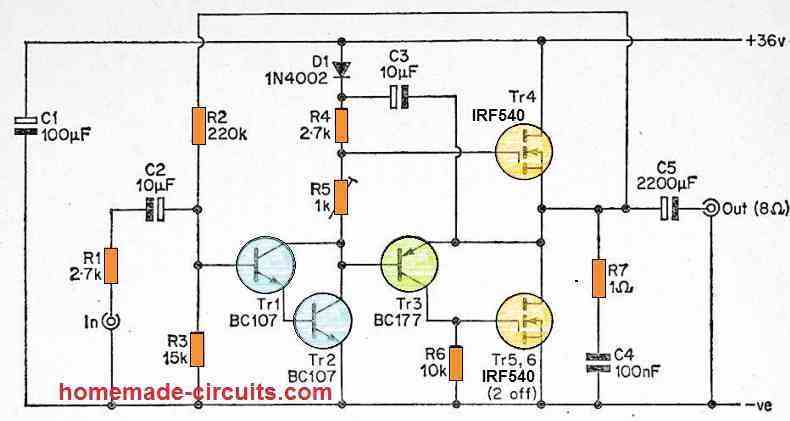
The Darlington pair emitter follower works without inversion of phase and provides a voltage gain of about unity. There is no net phase shift since the two emitter follower amplifiers individually create a phase inversion.
They effectively yield around unity voltage gain as a result of a high degree of feedback. Consequently, this approach produces a fairly nice and symmetrical outcomes, even though genuine complimentary configurations are now feasible and commonly implemented.
Tr4 essentially substitutes the Darlington emitter follower stage in this circuit, Tr5/6 is the common source output transistor, and Tr3 is the common emitter complementary transistor for Tr5/6. R6 serves as Tr3's collector load, and obtaining 100 percent negative feedback is as simple as connecting Tr3's emitter to the amplifier's output.
Disadvantage of using MOSFETs
One disadvantage of this configuration with a MOSFET device is that the threshold voltage of a MOSFET is greater than that of a BJT, requiring a very large gate to source voltage to push a MOSFET device firmly into the on mode.
Tr3 is used to generate the gate voltage for Tr5—6 from the amplifier's output.
To turn the amplifier's output entirely negative, Tr5-6 needs to have a very large gate to source voltage so that it is biased strongly on, however as the output of the amplifier switches more negatively, the highest gate to source value that Tr5-6 can reach decreases.
This causes the overall efficiency of the amplifier to be just ordinary.
Solution
One solution for mitigating this issue, and the one implemented in this design, is to combine a pair of MOSFET devices in parallel, across the common source position of the output stage.
This decreases the gate bias voltage needed for a specific output current, improving efficiency by allowing the output voltage swing to reach as near as possible to the negative supply rail voltage.
The remaining circuit configuration is basic, with Tr1 and Tr2 serving as the foundation for a Darlington common emitter driver stage. R5 is used to establish the necessary current through the output transistors during the quiescent conditions, and D1 and C3 provide bootstrapping, allowing Tr4 to operate with a maximum efficiency.
Power Supply
The circuit provides similar efficiency to Figure 2 with a supply voltage of approximately 36 volts approximately, although with a somewhat reduced gain and input impedance.
For highest output, a slightly more than 500mV RMS may be required at the input, and the input impedance is around 15k.
Another Simple 10 watt amplifier design
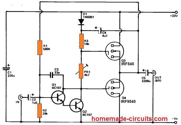
R1 and R2 are utilized to bias the unit to produce the best quiescent output voltage level and net negative feedback, that enhances the output reproduction performance.
D1 and C4 are boot-strapping components that allow the gate drive voltage to Q3 to exceed the positive supply voltage, increasing the circuit's efficiency.
Q2's main collector load is R3, while PR1 is utilized to provide a resting bias on the output transistors, resulting in a quiescent current intake of around 25mA.
Because MOSFET devices are not vulnerable to thermal runaway, the thermal compensation circuitry is completely unneeded in this design.
In reality, when the output MOSFETs become hot, the quiescent bias current drops significantly, although not enough to cause substantial crossover distortion.
C1 is a supply decoupling component, whereas C2 and C5 offer DC blocking at the input and output, correspondingly. C3 contributes to the circuit's stability by attenuating high frequencies.
Despite the fact that the current in the driver stage is only approximately 1mA, it should be enough because MOSFETs have exceptionally high input impedances and use no substantial input current. This is one of their primary benefits compared to the BJTs.
One drawback of this amplifier circuit is its poorer efficiency owing to greater threshold voltages, and higher on resistance of MOSFETs when compared to bipolar devices.
Nonetheless, with a supply voltage of around 33 V or such, the circuit can provide an output of 10 Watt rms (with a current consumption of up to approximately 600mA). For peak power, an input of around 500mV rms is required.
Using Power Transistors
When driven from a 30 volt source, the next design demonstrates a somewhat more complicated audio power amplifier that can provide roughly 10 watts into an 8-ohm loudspeaker.
Four high-gain, quasi-complementary output stages are included in this circuit (Q3 to Q6). In this circuit, transistor Q1 serves as a variable amplified diode output biasing device. C2 bootstraps and R3 DC biases the primary load resistor R2 of the Q2 common-emitter amplifier stage.
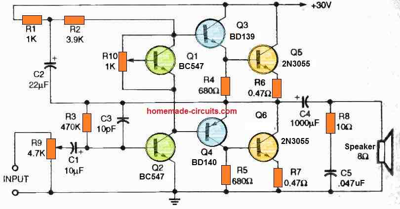
The quiescent output voltage of this circuit should be adjusted to around half of the dc power value. If this doesn't happen, you may change R3's value.
The amplifier's higher frequency response is limited by C3, which improves circuit stability. Furthermore, to improve circuit stability, capacitor C5 is linked in series with R8 across the amplifier's output.
Preset R10 is used for adjusting the quiescent current limit of the circuit.
10 watt Amplifier using BD131 and BD132 Transistors
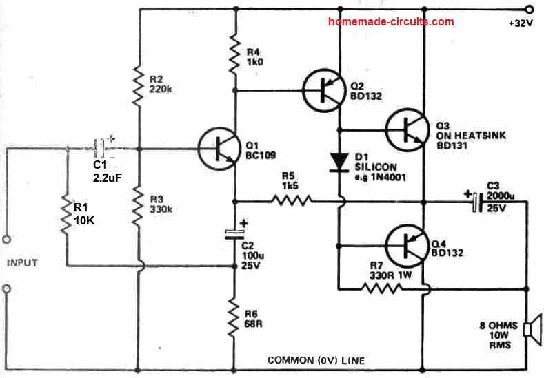
This general-purpose amplifier is really straightforward and reasonably priced. The sole unique aspect of the design is that the output transistors are under-biased.
This indicates that thermal runaway is not a possibility.
However, despite the fact that it should significantly increase distortion, the distortion is really rather minimal thanks to the strong usage of negative feedback. The frequency response is excellent.
10 Watt Amplifier using just 4 BJTs
Here is a straightforward and cost-effective audio power amplifier design that efficiently produces 10 watts of output power while utilizing just.
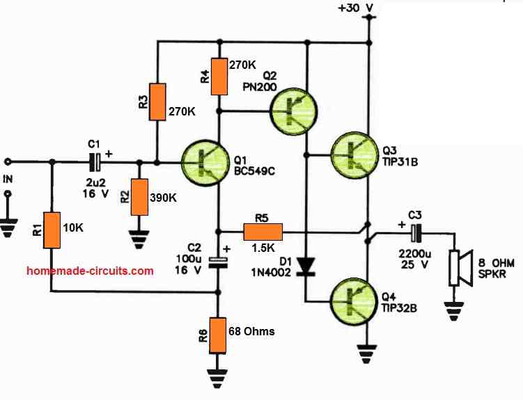
The output stage operates at a +30 V supply voltage and employs complementary output transistors that are deliberately underbiased.
The incorporation of a substantial amount of negative feedback, courtesy of R5, effectively mitigates the potential crossover distortion that could otherwise occur.
Transistors Q3 and Q4 are of the tag-type variety and should be mounted on a compact heatsink. These transistors have a construction that allows them to be securely fastened with just a single bolt.
Additionally, diode D1 can be affixed in place between them using epoxy to provide a degree of thermal feedback, even though the deliberate underbiasing of Q3 and Q4 helps prevent thermal runaway issues. This amplifier design is both uncomplicated and economical while delivering respectable output power.
Swagatam, I noticed in the 10 Watt amplifier using BD131 and BD132 that it has two problems, number one the power transistors are over-biased, according to
http://www.datasheetarchive.com they have an HFE of 20 to 40, a maximum collector current of 3 Amps, and a maximum Power dissipation of 15 Watts. The second problem is for true class AB operation there should be TWO diodes between the bases of the power transistors, this forces them to “split” the supply voltage equally across them, this also applies to the 10 Watt amplifier using just 4 BJTs.
Thank you Clair, You are absolutely right, there should be two diodes in series between the bases of the power transistors. I greatly appreciate your kind analysis. I hope the readers will take note of it…
Greetings
Hi Sir,
I saw your simple mosfet base amp 10wtt power. let me know the configuration sir this one class A or class AB? expecting your Express reply.
Thank you.
Hi, Dr.Sison,
To me it looks like most of them are class AB type.
Hello,
I tried to connect the first MOSFET amplifier circuit, with 2N2907 replacing BC177, and C1 with a 2200uF capacitor. The power supply is at 20V. The sound is good but the noise from the mains is horrible and I have difficulties in adjusting R8 (R8 is an 22kohm trimmer). If R8 is too large than the power of both MOSFETs would be running out of control, but if R8 is too small then the distortion is large. Could you suggest how to eliminate the noise and also how to adjust R8? Thank you.
Hello,
Glad you could build the first circuit successfully.
I think the R8 in the first diagram is for setting up the quiescent current or the idle current of the circuit.
You can adjust it by implementing the following steps:
Short circuit the input connections.
Short circuit the output connections.
Connect an ammeter in series with the positive supply line.
Switch ON power.
Now adjust the R8 preset until you find the ammeter showing zero current. That’s all.
To eliminate the HUM sound you may have to employ a good quality power supply, clamp the amplifier ground with the power supply metal body. You can also consider using a notch filter.
https://www.homemade-circuits.com/simple-hum-filter-circuit-for-amplifiers/
Hello,
I found the source of noise is from a valve pre-amp. However my other amplifiers (e.g. ACA MOSFET) do not have the same level of noise when connecting to that valve.
I tried to adjust R8 according to your method. It is not possible to have a zero current, and so I start from a smaller resistance and increase it until the current just meet the minimum (~16 mA). However when playing music, sometimes the power burst from less than 1 W to a very high value (>50 W, I use a watt meter to monitor the power of the supply) that the power supply (from an old laptop) cut it automatically. For smaller value of R8 is better, but still cannot totally avoid. Is it related to some faulty parts (e.g. the MOSFET)? Thank you.
Hello,
Try to reduce the input signal and check if that helps to reduce the noise or not.
If possible please add a volume control at the input side between the preamp and the amp.
16mA quiescent current is i think acceptable.
I don’t think the issue may be related to a faulty MOSFET.
Hello,
Finally I managed to get it works: remove the MOSFETs from the circuit board, use a fixed 10k for R8, connect the loudspeakers and input before connecting 24 V power supply (otherwise the power will be huge). No heat sink is needed for the MOSFET and the output power is not large but is enough for me. The noise is sometimes large and the power seems to increases with the noise. For safety purpose I connected a 1A fuse between the power supply and the amplifier.
Hi,
Thanks for updating the results, glad the problem to solved.
Sir
I am working technical Asst in kiit deemed university u know about working of technical staff .our experiment is audio amplifier using BJT ,mic and speaker please send function circuit working circuit diagram and audio oscillator circuit diagram. In mail address
Dibakar, how much maximum power output do you want from the amplifier?
Hi Swagatam;
I met the PC external sound card circuits in which ICs like pcm2704 and pcm2904 were used. Also I have one in my hand very simple model of HF002C. When getting closer look inside, I realized that it has very simple circuits parts and there are 9 pcs of capacitors and 1 diode and 1 resistor and after the USB connection, there is also very small part like 555 chip but over covered by the black seal. I think by regarding the USB output has 4 pins it is obvious that 2 of the USB pins are sound data pins. So, can we use any amplifier circuits (input voltage should be 5 V?) connected directly to PC USB output? Best Regards.
Hi Suat,
I think that may be possible. We can use any 5V amplifier and use it as a sound card. However, you will have to configure the pinouts of the amplifier correctly so that matches the USB pinouts.
Swagatam thanks for the response and the support.
However I have already circuit with the TDA2030 in my hand. Please advise if it would be remedy. But it’s input voltage is 12 V. So then I may use an external 12 V transformer and sound data from the PC USB. But in case that is impossible and I have to use 5 V of the USB then I need simpler one i.e. with 555 chip rather than LM4871 since unfortunately I will not find this IC in my residence area. Please share your opinion on the matter. Best Regards.
Hi Suat,
Actually I am not sure what kind of processing is needed for the USB audio output. If the the output is in the form of digital data then unfortunately an ordinary audio amplifier cannot be used.
You can try the TDA2030 with 12V, and connect with the USB. Makes sure to connect the ground of the USB with the ground of your amplifier….but remember not to touch the +12V to the USB anywhere.
After this you can investigate which is the audio output from the USB and connect that with the amplifier’s audio input. If the USB audio is not in the form of complex digital data then it should work
Thanks Swagatam;
After sending the message I thought the same to connect ground as common and also I thought I may add external 7 V to USB 5 V as totally 12 V. (nevertheless I need your confirmation) On the other hand I can see the pins of 1 and 4 are voltage pins of the USB output and 2 and 3 are the data pins but I should distinguish the – / +. Best Regards
Hi Suat, if you are using an external 12V to the amplifier then you must keep the USB 5V unconnected. Please do not connect anything on the 5V line of the USB. You just have to connect the ground or (-) lines of the USB and your amplifier circuit together. But I am not sure about the data pins, which pin needs to go connect with the amplifier input??
Como ajusto la corriente en reposo en este circuito.El menor voltaje que me entrega R5 es 12v al gate del mosfet. Tengo experiencia en los ajustes de los circuitos de fuente doble, como lo ajusto en este. Gracias por la ayuda
You will have to connect the input and output terminals both with the ground line, then connect a 12V flashlight bulb in series with the positive line os the amp, then switch ON power, and then adjust the preset until the bulb complete shuts off.
Muchas gracias hermano. Saludos desde cuba
It is my pleasure Yainobis!
Friend, I tried the circuit of the alternative amplifier with the p6nc60 mosfets, the amp works for several seconds and then makes a noise and gets very hot. what could it be
Hi, did you adjust the R5 preset correctly, which sets the quiescent current level of the amplifier?
How do I adjust the quiescent current in this circuit? The lowest voltage that R5 gives me is 12v to the gate of the mosfet. I have experience adjusting dual source circuits like I adjust in this one. Thanks for the help
You can connect a small 12V flashlight bulb in series with the positive line of the amplifier, short circuit the input, and the output terminals with the ground line….switch ON power. You may find the 12V bulb is glowing. Now start adjusting the R5 preset until the glow on the bulb completely shuts off….that all.
Gracias hermano. Ajustando R5 con 1k el menor voltaje que me da son 9 v en salida
I agree with you, but you will have to adjust the amplifier current by connecting a bulb with the input supply, as explained in the previous comment. Checking voltage might not help.
Can use IRF530 and IRF9530?
yes you can use them….