In this article I have explained how to make a multilevel (5 step) cascaded inverter circuit using a very simple concept developed by me. I have explained more regarding the details.
The Circuit Concept
In this website so far I have developed, designed and introduced many sine wave inverter circuits using straightforward concepts and ordinary components such as IC 555, which happen to be more result oriented instead of being complex and full of theoretical jumbles.
I have explained how simply a high power audio amplifier can be converted into a pure sine wave inverter, and I have also covered comprehensively regarding sine wave inveters using SPWM concepts
We have also learned through this website regarding how to convert any square inverter into a pure sine wave inverter design.
Assessing the above sine wave inverter circuits using sine equivalent PWMs, we understand that the waveform of SPWMs do not directly match or coincide with an actual sinusoidal waveform, rather these execute the sine wave effect or results by interpreting the RMS value of the actual sine wave AC.
Although SPWM can be considered an effective way of replicating and implementing a reasonably pure sine wave, the fact that it does not simulate or coincide with a real sine wave makes the concept a little unsophisticated, especially if compared to a 5 Level cascaded sine wave inverter concept.
We can compare and analyze the two types of sine wave simulation concepts by referring to the following images:
Multilevel Cascaded Waveform Image
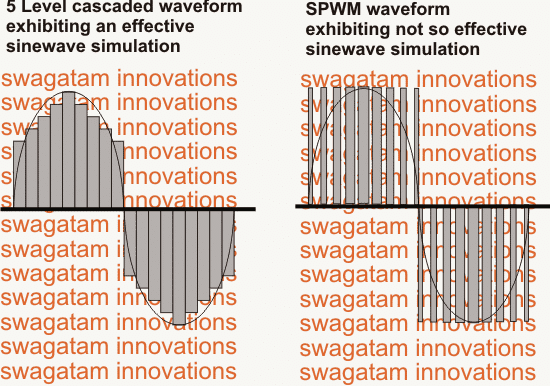
We can clearly see that the multilevel 5 step cascaded concept produces a more obvious and effective simulation of a real sine wave than the SPWM concept which relies solely on matching the RMS value with the original sine wave magnitude.
Designing a conventional 5 Level Cascaded sine wave Inverter can be quite complex, but the concept which is explained here makes the implementation easier and employs ordinary components.
Circuit Diagram
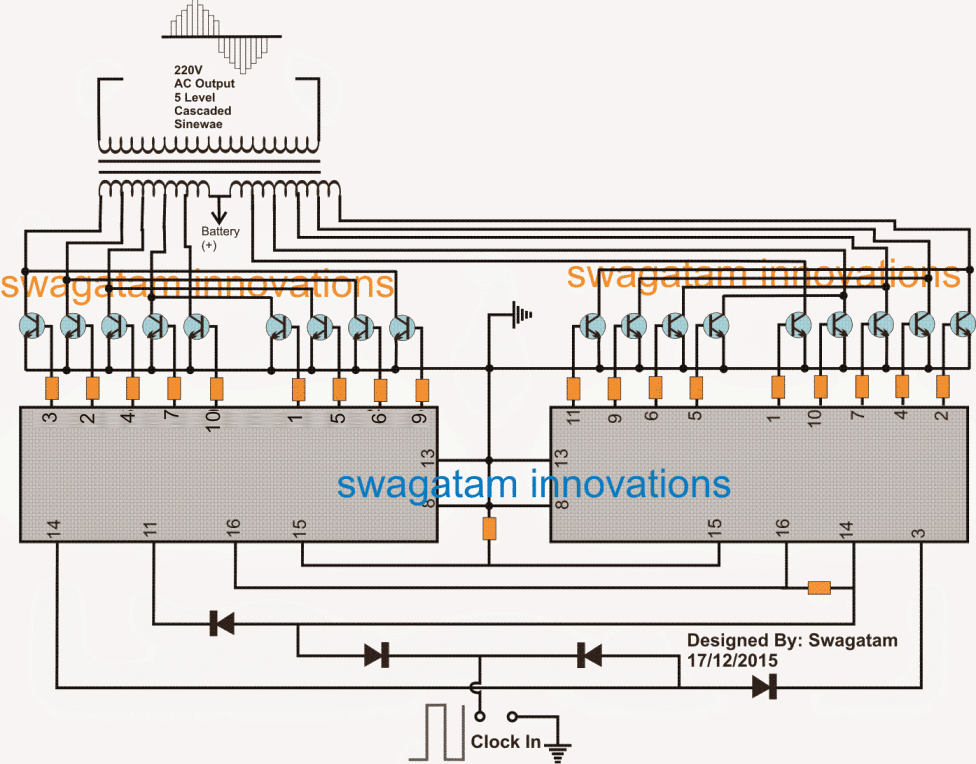
NOTE: Please add a 1uF/25 capacitor across pin#15 and pin#16 lines of the ICs, otherwise the sequencing will not initiate.
Referring to the image above, we can see how simply the 5 level cascaded inverter concept can be practically implemented using just a muti-tap transformer, a couple of 4017 ICs and 18 power BJTs, which could be easily replaced with mosfets if required.
Here a couple of 4017 ICs which are Johnson's 10 stage counter divider chips, are cascaded to produce a sequentially running or chasing logic highs across the shown pinouts of the ICs.
Circuit Operation
These sequentially running logic are used for triggering the connected power BJTs in the same sequence which in turn switch the transformer winding in an order which causes the transformer to produce a cascaded kind of sine equivalent waveform.
The transformer forms the heart of the circuit and employs a specially wounded primary with 11 taps. These taps are simply extracted uniformly from a single long calculated winding.
The BJTs associated with one of the ICs switch one of the halves of the transformer through 5 taps enabling the generation of 5 level steps, constituting one half cycle of the AC waveform, while the BJTs associated with the other ICs does the identical function to shape up the lower half AC cycle in the form of 5 level cascaded waveform.
The ICs are run by clock signals applied to the indicated position in the circuit, which could be acquired from any standard 555 IC astable circuit.
The first 5 sets of the BJTs build up the 5 levels of the waveform, the remaining 4 BJTs switch the same in reverse order to complete the cascaded waveform having a total of 9 skyscrapers.
These skyscrapers are formed by producing an ascending and descending voltage levels by the switching of the corresponding winding of the transformer which are rated at the relevant voltage levels
For example, winding #1 could be rated at 150V with respect to the center tap, the winding #2 at 200V, winding #3 at 230V, winding #4 at 270V and winding #5 at 330V, so when these are switched sequentially by the set of the shown 5 BJTs, we get the first 5 levels of the waveform, next when these winding are switched in reverse by the following 4 BJTs it creates the descending 4 level waveforms, thus completing the upper half cycle of the 220V AC.
The same is repeated by the other 9 BJTs associated with the other 4017 IC giving rise to the lower half of the 5 level cascaded AC, which completes one complete AC waveform of the required 220V AC output.
Transformer Winding Details:
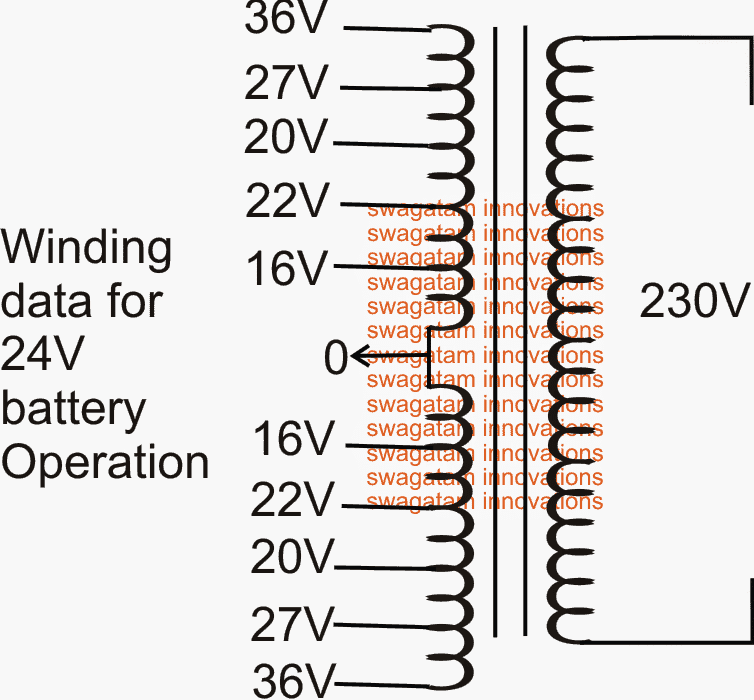
As may be witnessed in the above diagram, the transformer is an ordinary iron core type, made by winding the primary and the secondary with turns corresponding to the indicated voltage taps.
When connected with the corresponding BJTs these winding can be expected to induce a 5 level or a total of 9 level of cascaded waveform wherein the first 36V winding would correspond and induce a 150V, the 27V would induce an equivalent of 200V, while the 20V, 27V, 36V would be responsible of producing 230V, 270V and 330V across the secondary winding in the proposed cascaded format.
The set of taps on the lower side of the primary would carry out the switching to complete 4 ascending levels of the waveform.
An identical procedure would be repeated by the 9 BJTs associated with the complementary 4017 IC for building the negative half cycle of the AC...the negative is rendered due to the opposite orientation of the transformer winding with respect to the center tap.
Update:
Complete circuit diagram of the discussed multi-level sinewave inverter circuit
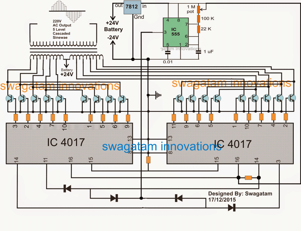
NOTE: Please add a 1uF/25 capacitor across pin#15 and pin#16 lines of the ICs, otherwise the sequencing will not initiate.
The 1M pot associated with the 555 circuit will need to be adjusted for setting up a 50Hz or a 60Hz frequency for the inverter as per the country specs of the user.
Parts List
All unspecified resistors are 10k, 1/4 watt
All diodes are 1N4148
All BJTs are TIP142
ICs are 4017
Notes for the Multilevel 5 Step Cascaded Sine Wave Inverter Circuit:
The testing and verification of the above design was successfully conducted by Mr. Sherwin Baptista, who is one of the keen followers of the website.
1. We decide the input supply to the inverter---24V @ 18Ah @ 432Wh
2. There will be an issue of NOISE generated in the whole process of building this inverter. To crack the issue of noise generated and amplified very easily;
A. We decide to filter the output signal of IC555 the moment it is produced at pin 3, by doing so a cleaner square wave can be obtained.
B. We decide to use FERRITE BEADS at the respective outputs of IC4017 to enhance filtering before the signal is sent to the amplifier transistors.
C. We decide to use TWO TRANSFORMERS and enhance filtering between both of them in the circuit.
3. The Oscillator Stage Data:
This proposed stage is the main stage of the inverter circuit. It produces the required pulses at a given frequency for the transformer to operate. It consists of IC555, IC4017 and Amplifier Power Transistors.
A. IC555:
This is an easy to use low power timer chip and has plenty of variety of projects that can be done using it. In this inverter project we configure it in astable mode to generate square waves. Here we set the frequency at 450Hz by adjusting the 1 megaohm potentiometer and confirming the output with a frequency meter.
B. IC4017:
This is a Jhonson's 10 stage counter divider logic chip which is very famous in sequential/running LED flasher/chaser circuits. Here it is smartly configured to be used in an inverter application. We provide this 450Hz generated by IC555 to the inputs of IC4017. This IC does the job of breaking the input frequency into 9 parts with each resulting in a 50Hz output.
Now the output pins of both 4017's are having a clock signal of 50Hz continuously running forward and backward.
C. The Amplifier Power Transistors:
These are the High Power Transistors which pull the battery power into the transformer windings with accordance to the signal fed into them. Since the output currents of the 4017s are too low, we cannot directly feed them into the transformer. Therefore we need some kind of amplifier which will convert the low current signals from the 4017s into high current signals which then can be passed onto the transformer for further operation.
These transistors would get hot during operation and would necessarily need heatsinking.
One could use a separate heatsinks for each transistor, hence it should be ensured that the
heatsinks do not touch each other.
OR
One could use a single long piece of heatsink to fit all the transistors on it. Then one should
thermally and electrically isolate each transistor's center tab from touching the heatsink in
order to avoid them from getting shorted. This can be done by using Mica Isolation Kit.
4. Next comes the First Stage Transformer:
A. Here we employ the Multi-tapped Primary to a Two Wire Secondary transformer. Next we find the volts per tap to prepare the primary voltage.
---STEP 1---
We take into consideration the Input DC Voltage that is 24V. We divide this with 1.4142 and find its AC RMS equivalent which is 16.97V~
We round the above RMS figure which results in 17V~
---STEP 2---
Next we divide RMS 17V~ by 5(since we need five tap voltages) and we get RMS 3.4V~
We take the final RMS figure by 3.5V~ and multiplying it by 5 gives us 17.5V~ as a round figure.
In final we found the Volts Per Tap which is RMS 3.5V~
B. We decide to keep the Secondary voltage to RMS 12V~ i.e., 0-12V is because we can obtain a higher amperage output at 12V~
C. So we have the transformer rating as below:
Multi-tapped Primary: 17.5---14---10.5---7---3.5---0---3.5---7---10.5---14---17.5V @ 600W/1000VA
Secondary: 0---12V @ 600W/1000VA.
We got this transformer wound by a local transformer dealer.
5. Now follows the main LC Circuit:
An LC circuit being known as a filter device has robust applications in power converter circuits.
Being used in an inverter application it is generally required for breaking down the sharp peaks
of any generated waveform and helps convert it into a smoother waveform.
Here at the secondary section of the above transformer being 0---12V, we expect a multilevel
square cascaded waveform at the output. So we employ a 5 Stage LC Circuit to get a SINEWAVE equivalent waveform.
The data for the LC Circuit is as below:
A) All Inductors should be a 500uH(microhenry) 50A rated IRON CORE EI LAMINATED.
B) All Capacitors should be a 1uF 250V NONPOLAR type.
Note that we stress on the 5 stage LC circuit and not just one or two stages such that we can get a much cleaner waveform at the output with lesser harmonic distortion.
6. Now comes the Second and Final Stage Transformer:
This transformer is responsible for converting the output from the LC network i.e., RMS 12V~ to 230V~
This transformer would be rated as below:
Primary: 0---12V @ 600W/1000VA
Secondary: 230V @ 600W/1000VA.
Here, NO additional LC network would be required at the final 230V output for more filtering since we already filtered every stage of each processed output at the beginning.
The OUTPUT will now be a SINEWAVE.
A GOOD thing is that there is absolutely NO NOISE at the final output of this inverter and
sophisticated gadgets can be operated.
But one thing to be kept in mind by the person operating the inverter is NOT TO OVERLOAD THE INVERTER and keep the power loads of sophisticated gadgets being operated in limits.
A few corrections to be made in the circuit diagram are given as under:
1. The IC7812 regulator should have bypass capacitors connected. It should be mounted on a
HEATSINK since it would get warm during operation.
2. The IC555 timer should follow a series resistance before it's signal passes forward to diodes.
The value of resistance should be 100E. IC gets hot if the resistor is not connected.
In Conclusion we have 3 proposed filter stages:
1. The signal generated by IC555 at pin 3 is filtered to ground and then passed on to resistor
and then to the diodes.
2. As the running signals exit the relevant pins of IC4017, we connected ferrite beads before
passing signal to resistor.
3. The final filter stage is employed between both transformers
How I Calculated the Transformer Winding
I would want to share something with you today.
When it came to winding iron core, i knew nothing about rewinding specifications since i found out a lot of parameters and calculations go into them.
So for the above article i gave the basic specs to the trafo winder person and he just asked me:
a) The input and output voltage; tapping if necessary,
b) The input and output current,
c) The total power,
d) Do you need external clamping fixture bolted to the trafo?
e) Do you want a fuse connected internally in the transformer 220V side?
f) Do you want wires connected to the trafo OR simply keep the enameled wire on the outside with added heatsink material?
g) Do you want the core to be grounded with an external wire connected?
h) Do you want the IRON CORE to be protected; varnished and painted with black oxide?
Finally he assured me of a complete safety test for the transformer being a made-to-order type once ready and it will take a span of 5 days to get completed till a part payment is provided.
The part payment were (on an approx.) one fourth of the total proposed cost dictated by the winder person.
My answers to the above questions are:
NOTE: To avoid wiring confusions, i assume trafo is made for one purpose: STEP DOWN TRANSFORMER where primary is high voltage side and secondary is low voltage side.
a) 0-220V primary input, 2-wires.
17.5---14---10.5---7---3.5---0---3.5---7---10.5---14---17.5V secondary multi-tapped output, 11-wires.
b) The primary input current: 4.55A at 220V The output current: 28.6 Amps on multi-tapped secondary @ end to end voltage 35V…..where calculation is concerned.
I told him i need 5 amps at 220V(230. max) i.e., primary input and 32 amps at 35V i.e., multi-tapped secondary output.
c) I initially told him 1000VA but based on volt times amp calculation and rounding off decimal figures, the power went to 1120VA +/-10%. He provided me with a safety tolerance value for the 220V side.
d) Yes. I do need for easy fixture onto metal cabinet.
e) No. I told him i will place one externally for easy access of it when it accidentally blows off.
f) I told him to keep the enameled wire on the outside for the multi-tapped secondary side being appropriately heatsinked for safety and on the primary side i requested wires to be connected.
g) Yes. I need the core to be earthed for safety reasons. Therefore please attach an external wire.
h) Yes. I requested him to provide the necessary protection for the core stampings.
These were the interaction between me and him for the proposed made-to-order type transformer.
UPDATE:
In the above 5 step cascaded design we implemented the 5 step chopping across the DC side of the transformer, which appears to be a bit inefficient. It's because the switching could result in a significant amount of power lost through back EMF from the transformer, and this will need the transformer to be enormously big.
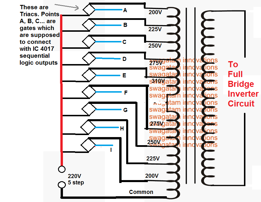
A better idea could be to oscillate the DC side with a 50 Hz or 60 Hz full bridge inverter, and switch the secondary AC side with our 9 step sequential IC 4017 outputs using triacs, as shown below. This idea would reduce spikes and transients and enable the inverter to have a smoother and efficient execution of the 5 step sine waveform. The triacs will be less vulnerable to the switching, compared to the transistors at the DC side.
