In this article I will elucidate many assorted circuit ideas built using NAND gates from ICs such as IC 7400, IC 7413, IC 4011, and IC 4093 etc.
IC 7400, IC 7413 Specifications
The I.C.s 7400 and the 7413 are 14 -pin DIL ICs, or "14 pin Dual In Line Integrated Circuits", where pin 14 is the positive supply V+ and pin 7 is the negative, ground or 0 V pin.
Supply inputs to pins 14 and 7 are not shown in the drawings for simplicity sake, but you are advised not to forget to connect these pins, or else the circuit would simply fail to work!
All the circuits work using a 4.5 V or 6 V DC supply however the typical voltage can be 5 volts. A mains driven 5 V regulated supply can be obtained through a number of options.

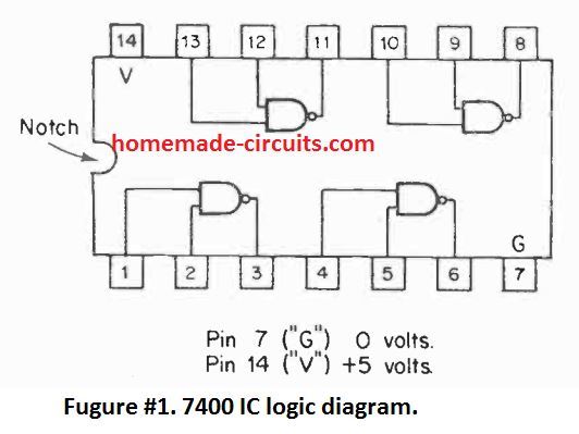
The 4 gates of a 7400 are exactly the same with their specs:
- Gate A pins 1, 2 inputs, pin 3 output
- Gate B pins 4, 5 inputs, pin 6 output
- Gate C pins 10, 9 inputs, pin 8 output
- Gate D pins 13, 12 inputs, pin 11 output
You may find a specific circuit indicating an oscillator applying gates A and B, however this also means that the same can be designed using gates A and C, B and C or C and D also, without any problems.
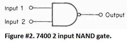
Figure 1 exhibits the logic circuit of your 7400 I.C. Figure 2 demonstrates the logic symbolic representation for just one gate, every single gate usually a "2 Input NAND Gate".
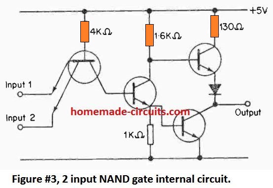
The internal configuration with an individual gate is displayed in figure 3. The 7400 is a TTL logic I.C., that means it works by using "Transistor-Transistor-Logic". Every single gate employs Four transistors, every 7400 is made up of 4 x 4= 16 transistors.
The logic gates include a pair of states, depending on the binary system, 1 or "High" typically 4 volts, and 0 (zero) or "Low" typically 0 volts. In case a gate terminal is not used. that may correspond to a 1 input.
Meaning an open gate pin is at "high" level. When a gate input pin is connected with the ground or 0 volts line, the input then becomes 0 or logic low.
A NAND gate is actually a mix of "NOT and AND" gate when both of its inputs (and function) are at logic 1, output is a NOT gate output which is 1.
The output from a NOT gate will be 0V in response to a 1 input signal or + supply input, meaning output will be logic Zero when input is at + supply level.
For a NAND gate when both inputs are logic 0, output turns into logic 1, which is exactly like a NOT gate response. It might look difficult to comprehend exactly why the output is 1 when inputs held at 0, and vice versa.
It can be explained in this way
For a switching of state an AND function must come about, that is each inputs must transform for the toggling of state.
This solely happens when the two inputs switch through 0 to 1. The 7400 gates are 2 input NAND gates however 3 input NAND gates 7410 I.C., 4 input NAND gates 7420 and also an 8 input NAND gate 7430 can be also procured easily from the market.
Regarding the 7430, its 8 input gate will switch state only when each one of the 8 inputs are either 1 or 0.
When the 8 inputs of the 7430 are 1,1,1,1,1,1,1,0 then the output will continue to be 1. The change of state will not occur as long all 8 inputs do not have the identical logics.
But as soon as the last input changes from 0 to 1 the output changes from 1 to 0. The technique that causes "change of state" is a crucial aspect to understand the functionality of logic circuits.
The number of pins a logic IC may commonly have are 14 or 16. A 7400 consists of four NAND gates, with 2 input pins and 1 output pin for each of the gates, and also a pair of pins for the power supply inputs, pin 14 and pin 7.
IC 7400 Family
The other members of the 7400 family may come with higher number of input pins such as 3 input NAND gates, 4 input NAND gates and the 8 input NAND gate featuring more input combination options for each gate. As an example the IC 7410 is a variant of 3 input NAND gates or a"Triple 3 input NAND gate".
The IC 7420 is a variant of 4 input NAND gates and is also called "Dual 4 input NAND gate" while the IC 7430 is a member that has 8 inputs and is known as 8 -input NAND gate.
Basic NAND Gate Connections
While the IC 7400 features only NAND gates, it is possible to connect the NAND gates in a number of ways.
This allows us to convert them into other forms of gate like:
(1) an inverter or "NOT" gate
(2) an AND gate
(3) an OR gate
(4) NOR gate.
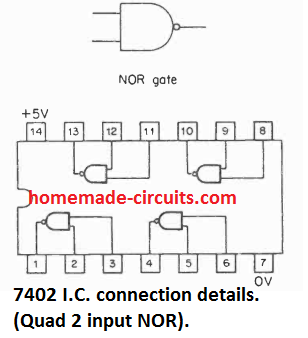
The IC 7402 resembles the 7400 although is made up of 4 NOR gates. In the same way as NAND is a combination of "NOT plus AND", NOR is blend of "NOT plus OR".
The 7400 is an extremely adaptable IC as can be found from the range following of circuits in the applications guide.
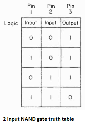
To help you fully grasp the functionality of a NAND gate, a TRUTH table is demonstrated above for a 2 input NAND gate.
Equivalent truth tables could be evaluated for just about any logic gate. The truth table for an 8 input gate like the 7430 is somewhat more complex.
How to Test a NAND Gate
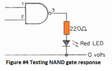
In order to check a 7400 IC, you can apply power across pins 14 and 7. Keep pins 1 and 2 connected to positive supply, this will show the output as 0.
Next, without changing pin 2 connection, connect pin 1 to 0 volts. This will enable the inputs to become 1, 0. This will cause the output to turn 1, illuminating the LED. Now simply, swap pin 1 and pin 2 connections, so that the Inputs become 0, 1, this will switch the output to logic 1, which will again keep the LED illuminated.
In the final step, connect both the input pins 1 and 2 to ground or 0 volts so that both the Inputs are at logic 0, 0. This will yet again turn the output to logic high or 1, switching ON the LED. The glowing of the LED signifies the logic level 1.
When LED is OFF this suggests logic level 0. The analysis could be repeated for the gates B, C and D.
Note: each of the circuits proven here work with 1/4W 5% resistors - all electrolytic capacitors are generally 25V rated.
If a circuit fails to work, you may look at the connections, the possibility of a faulty IC may be highly unlikely compared to an incorrect connection of the pins. This connections of a NAND gate shown below may be the most basic and works by using only 1 gate of a 7400.
1) NOT Gate from a NAND Gate
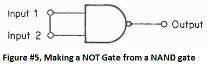
When the input pins a of a NAND gate are shorted with each other the circuit then works like an inverter, meaning the output logic shows always the opposite of the input.
When the shorted input pins of the gate is connected to 0V, the output will turn into 1 and vice versa. Because the "NOT" configuration provides an opposing response across the input and the output pins, hence the name NOT gate. This phrase is actually a technically appropriate one.
2) Creating AND Gate from a NAND Gate
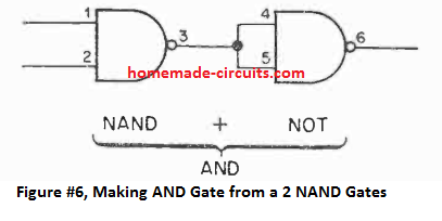
Since a NAND gate is also a kind of a "NOT AND" gate, therefore in case a "NOT" gate is introduced after a NAND gate, the circuit turns into a "NOT NOT AND" gate.
A couple of negatives produce a positive (a notion that's popular in math concepts too). The circuit has now become an "AND" gate as shown above.
3) Making OR Gate from NAND Gates
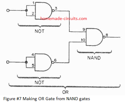
Inserting a NOT gate before each NAND gate inputs generates an OR gate as demonstrated above. This is usually a 2 -input OR gate.
4) Making NOR Gate from NAND Gates
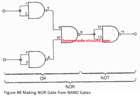
In the previous design we created an OR gate from NAND gates. A NOR gate in fact becomes a NOT OR gate when we add an extra NOT gate just after an OR gate as shown above.
5) Logic Level Tester
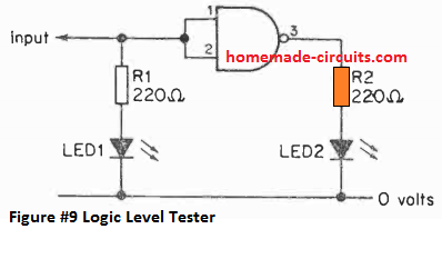
This logic level tested circuit can be created through a single 7400 NAND gate as an inverter or NOT gate for indicating logic levels. A couple of red LEDs are employed to distinguish the logic levels across the LED 1 and LED 2.
The LED pin which is longer becomes the cathode or the negative pin of the LED. When the input is at logic level 1 or HIGH, LED 1 illuminates naturally.
The pin 3 which is the output pin is the opposite of the input at logic 0 which causes the LED 2 to remain OFF. When the input gets a logic 0, LED 1 shuts OFF naturally, but LED 2 now glows due to the opposite response of the gate.
6) BISTABLE LATCH (S.R. FLIP-FLOP)
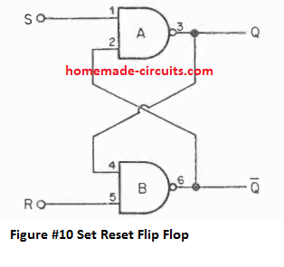
This circuit makes use of a couple of NAND gates cross-coupled, to make a S-R bistable latch circuit.
The outputs are marked as Q and 0. The line above the Q signifies NOT. The 2 outputs Q and 0 acts like complements of each other. Meaning, when Q reaches logic level 1, Q turns 0; when Q is 0, Q turns 1.
The circuit could be activated into both of the 2 stable states through an appropriate input pulse. Essentially this allows the circuit a "memory" feature and creates this into a super easy 1 bit (one binary digit) data storage chip.
The two inputs are branded S and R or Set and Reset, thus this circuit is usually known as S.R.F.F. (Set Reset Flip-Flop). This circuit can be quite useful and it is applied in a number of circuits.
THE S-R FLIP-FLOP RECTANGULAR WAVE GENERATOR
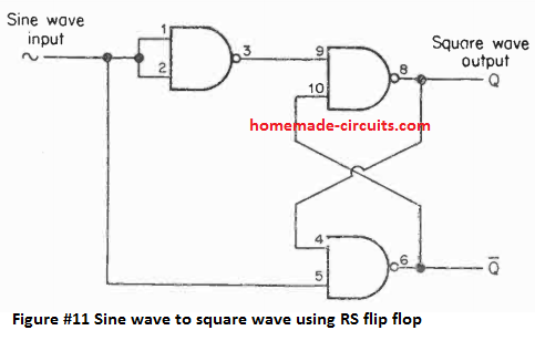
The SR Flip-Flop circuit can be configured to work like a square wave generator. If the F.F. is applied with a sine wave, let's say from a 12V AC from a transformer, with minimum 2 volts peak to peak range, the output will respond by generating square waves having peak to peak equivalent to the Vcc voltage.
These square wave can be expected to be perfectly square in shape due to the extremely fast rise and fall times of the IC. The inverter or NOT gate output feeding the to the R input results in creating complementary ON/OFF inputs across the R and S inputs of the circuit.
8) SWITCH CONTACT BOUNCE ELIMINATOR
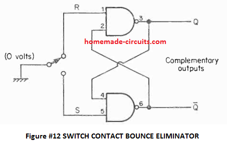
In this circuit an S-R FLIP-FLOP can be seen applied as a switch contact bounce eliminator.
Whenever switch contacts are closed it is usually followed by the contacts bouncing rapidly a few times between due to mechanical stress and pressure.
This mostly results in the generation of spurious spikes, which may cause interference and erratic circuit operation.
The above circuit eliminates this possibility. When the contacts close initially it latches the circuit, and due to this the interference from contact bounce fails to create any effect on the flip-flop.
9) MANUAL CLOCK
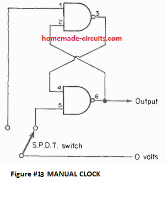
This is a another variant of circuit eight. For experimenting with circuits like half adder or other logic circuits, it really is necessary to be capable of analyzing the circuit since it works with a single pulse at a time. This could be achieved by the application of a hand operated clocking.
Whenever the switch is toggled a solitary trigger turns up at the output. The circuit works extremely well with a binary counter. Whenever the switch is toggled, only a single pulse at a time is allowed to happen due to anti-bounce feature of the circuit, enabling the count to progress one trigger at a time.
10) S-R FLIP-FLOP WITH MEMORY
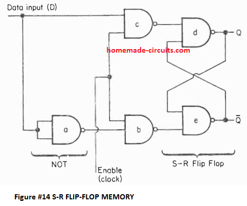
This circuit is designed using the basic S-R Flip-Flop. The output is determined by the last input. D indicates the DATA input.
An "enabling" pulse becomes necessary to activate gates B and C. Q forms the identical logic level as D, Meaning this assumes the value of D and continues to be in this condition (see picture 14).
The pin numbers aren't given for simplicity sake. All 5 gates are 2 input NAND, a couple of 7400s are needed. The diagram above only denotes a logic circuit, yet can be quickly converted into a circuit diagram.
This streamlines diagrams that include huge amounts of logic gates to work with. The enable signal could be a pulse from the "manual clock circuit" explained previously.
The circuit works whenever a "CLOCK" signal is applied, this is usually a basic principle employed in all computer related applications. The couple of circuits explained above may be built using just two 7400 ICs wired up with each other.
11) CLOCK CONTROLLED FLIP-FLOP
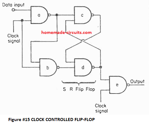
This is actually another type of SR flip flop with memory. The data input is governed with a clock signal, the output through the S-R Flip-Flop is likewise regulated by the clock.
This Flip-Flop works well like a storage register. The clock is actually a master controller for the input and output movement of pulses.
12) HIGH SPEED PULSE INDICATOR AND DETECTOR
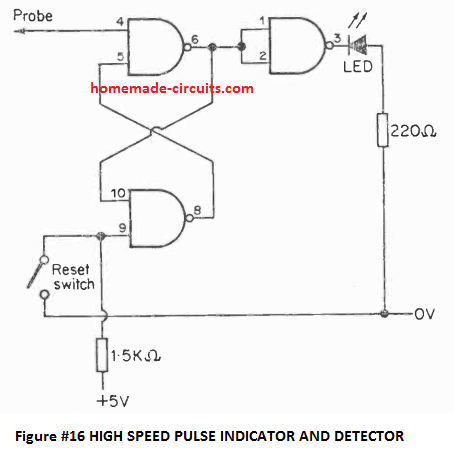
This particular circuit is designed using the S-R Flip -Flop and is accustomed to sense and display a specific pulse within a logic circuit.
This pulse latches the circuit, the output is then applied to the inverter input which causes red LED to glow.
The circuit continues to be in this particular state until it is eliminated by toggling the single pole switch, reset switch.
13) "SNAP!" INDICATOR
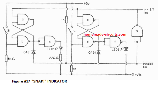
This circuit shows how to use of the S-R Flip -Flop in another way. Here, two flip-flops are incorporated through 7 NAND gates.
The fundamental theory in this circuit is the application of S-R flip-flops and the INHIBIT lines. S1 and S2 form the switches that govern the flip-flops.
The moment the flip-flop latches, the associated LED switches ON and the complementary flip-flop is prevented from latching. When the switches are in the form of push buttons, releasing the button causes resetting of the circuit. The diodes employed are 0A91 or any other will do such as 1N4148.
- Gates A, B, C form the stage for S1 and LED 1.
- Gates D, E, F constitute stage for S2 and LED 2.
- Gate G confirms that the INHIBIT and INHIBIT lines work like complementary pairs.
14) LOW FREQUENCY AUDIO OSCILLATOR
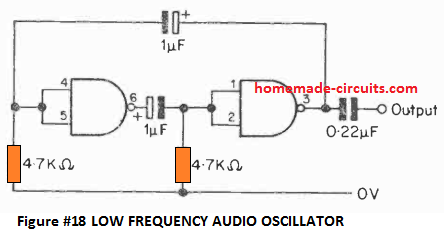
The circuit uses two NAND gates connected as inverters and cross coupled to form an astable multivibrator.
The frequency can be altered by increasing the value of CI and C2 (lower frequency) or decreasing the value of C1 and C2 (higher frequency). As electrolytic capacitors make sure the polarity connection is correct.
Circuits fifteen, sixteen and seventeen are also types of low frequency oscillators created from circuit fourteen. However, in these circuits the output is configured to make the LEDs flash.
We can observe that all these circuit resemble each other quite closely. However, in this circuit if an LED is used at the output will cause flashing of the LED at a very rapid rate which can be virtually indistinguishable by our eyes due to persistence of vision. This principle is used in pocket calculators.
15) TWIN LED FLASHER
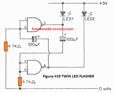
Here we incorporate a couple of NAND gates for creating a very low frequency oscillator. The design controls two red LEDs causing the LEDs to flash with alternate ON OFF switching.
The circuit works with two NAND gates, the remaining two gates of the IC could be additionally employed within the same circuit. Different capacitor values could be used for this second circuit to generate an alternate LED flasher stage. Higher value capacitors will cause the LEDs to flash slower and vice versa.
16) SIMPLE LED STROBOSCOPE
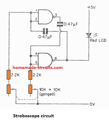
This specific design is produced out of circuit fifteen which works like a low power stroboscope. The circuit in fact is a high speed LED flasher. The red LED twitches fast but the eye struggles to distinguish the specific flashes (due to persistence of vision).
The output light cannot be expected to be too powerful which means that the stroboscope may work better only when it is dark, and not during day time.
The ganged variable resistors is used to vary the frequency of the strobe so that the stroboscope can easily adjusted for any desired strobe rate.
The stroboscope work extremely well at higher frequencies by modifying the timing capacitor value. The LED actually being a diode is able to support very high frequencies with ease. We recommend that it could possibly be applied to capture extremely high speed pictures through this circuit.
17) LOW HYSTERESIS SCHMITT TRIGGER
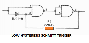
Two NAND gates function may be configured like a Schmitt trigger to create this specific design. In order to experiment with this circuit you may want to tweak R1 which is positioned for hysteresis effect.
18) FUNDAMENTAL FREQUENCY CRYSTAL OSCILLATOR
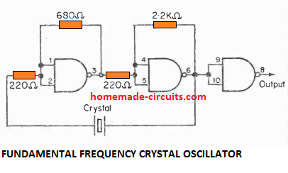
This circuit is rigged as a crystal controlled oscillator. A pair of gates are wired as inverters, the resistors provide the correct amount of biasing for the associated gates. The 3rd gate is configured like a "buffer" which prevents over loading the oscillator stage.
Remember that when a crystal is employed in this particular circuit, it is going to oscillate at its fundamental frequency, meaning, it won't oscillate at its harmonic or overtone frequency.
In case the circuit operates at a considerably reduced frequency than estimated, would imply that the crystal frequency is operating at an overtone. In other words, it may be operating with several fundamental frequencies.
19) TWO BIT DECODER
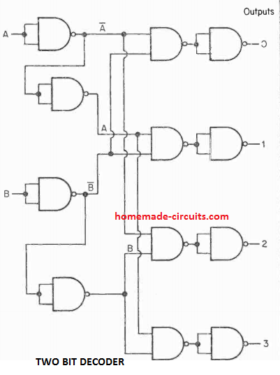
This circuit constitutes a simple two bit decoder. The inputs are across the line A and B, outputs are across the line 0, 1, 2, 3.
Input A can be as logic 0 or 1. Input B can be as logic 0 or 1. If A and B both are applied with logic 1, this becomes a binary count of 11 which is equal to denary 3 and the output across line 3 is "high".
Likewise, A, 0 B, 0 output line 0. The highest count is based on the amount of inputs. The greatest counter using 2 inputs is 22 - 1 = 3. It may be possible to extend the circuit further, for example if four inputs were employed A, B, C and D, in that case the highest count will be 24 - 1 = 15 and the outputs are from 0 to 15.
20) PHOTO SENSITIVE LATCHING CIRCUIT
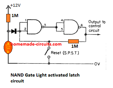
This is a simple photodetector based circuit which employs a couple of NAND gates to trigger a darkness activated latching action.
When the ambient light is higher than the set threshold, the output remains unaffected and at zero logic. When darkness falls below the set threshold, the potential at the input of the NAND gate toggles it to logic high, which in turn latches the output into a high logic permanently.
Removing the diode removes the latching feature and now the gates operates in tandem with the light responses. Meaning the output alternately goes High and LOW in response to the light intensities on the photodetector.
21) TWIN TONE AUDIO OSCILLATOR
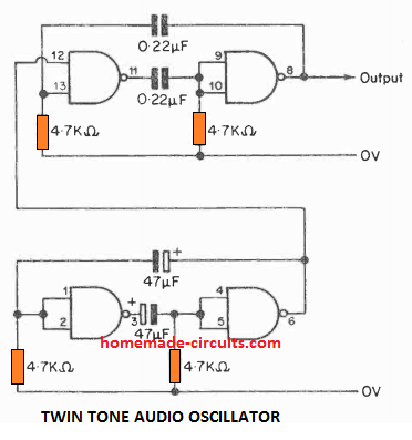
The next design shows how to build a a two tone oscillator using two pairs of NAND gates. Two oscillators stages are configured using this NAND gates, one having a high frequency using 0.22 µF, while the other with a low frequency oscillator 0.47 uF capacitors.
The oscillators coupled with each other together in a way that the low frequency oscillator modulates the high frequency oscillator. This produces a warbling sound output which sounds more pleasing and interesting than a mono tone produced by a 2 -gate oscillator.
22) CRYSTAL CLOCK OSCILLATOR
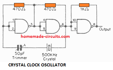
This is another crystal based oscillator circuit for use with a L.S.I. IC clock "chip" for a 50 Hz base. The output is adjusted at 500 kHz so to get 50 Hz, this output needs to be connected to four 7490 I.C.s in cascade manner. Each 7490 then divides the subsequent output by 10 enabling a total division of 10,000.
This finally produces an the output equal to 50 Hz (500,000 10 ÷ 10 ÷ 10+ 10 = 50). The 50 Hz reference is normally acquired from the mains line but using this circuit allows the clock to be independent from the mains line and also get an equally precise 50 Hz time base.
23) SWITCHED OSCILLATOR
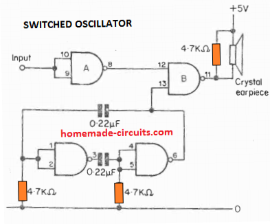
This circuit is made up of a tone generator and a switching stage. The tone generator operates non-stop, but without any kind of output on the earpiece.
However, as soon as a logic 0 appears at the input gate A, it inverts gate A to a logic 1. The logic 1 opens gate B and the sound frequency is allowed to reach the earpiece.
Even though a tiny crystal earpiece is employed here, this is still able to generate an amazingly loud sound. The circuit could possibly be applied like a buzzer featuring along side an electronic alarm clock I.C.
24) ERROR VOLTAGE DETECTOR
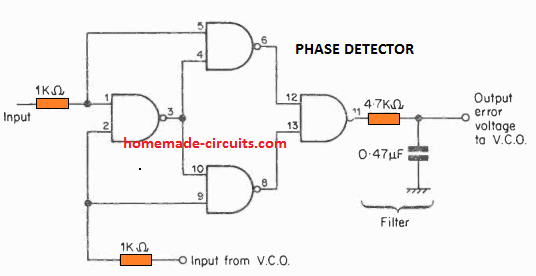
This circuit is designed to work as a phase detector through four NAND gates. The phase detector analyzes two inputs and generates an error voltage which is proportional to the difference between the two input frequencies.
The detector output converts the signal through an RC network comprising of a 4k7 resistor and a 0.47uF capacitor to produce a DC error voltage. The phase detector circuit works extremely well in a P.L.L. (phase lock loop) applications.
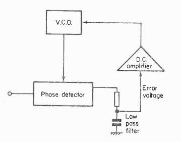
The above diagram shows a block diagram of a full P.L.L. network. The error voltage generated by the phase detector is boosted to regulate the multivibrator frequency of the V.C.O. (voltage controlled oscillator).
The P.L.L. is a incredibly useful technique and is very effective in F.M demodulation at 10.7 MHz (radio) or 6 MHz (TV sound) or to reestablish the 38 KHz subcarrier within a stereo multiplex decoder.
25) RF Attenuator
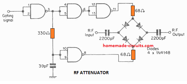
The design incorporates 4 NAND gates and applies them in a chopper mode for controlling the diode bridge.
The diode bridge switches either for enabling the conduction of the RF or for blocking the RF.
How much RF is allowed through the channel is ultimately determined by the gating signal. The diodes can be any high speed silicon diodes or even our own 1N4148 will work (see diagram 32).
26) REFERENCE FREQUENCY SWITCH
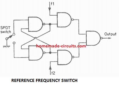
The circuit works with five NAND gates for developing a 2-frequency switch. Here, a bistable latch circuit is used along with a single pole switch for neutralizing the debouncing effect from the SPDT switch. The final output could be f1 or f2, depending on the position of the SPDT.
27) TWO BIT DATA CHECK
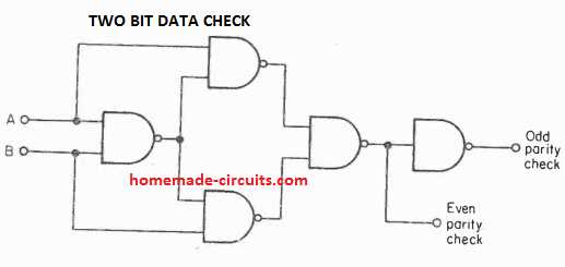
This circuit works with a computer type concept and can be used to learn the basic logic functions that arise in a computer, leading to errors.
Checking errors is performed with the addition of a supplementary bit (binary digit) in "words" in order that the final amount appearing in a computer "word" is consistently odd or even.
This technique is referred to as a "PARITY CHECK". The circuit examines odd or even parity for 2 bits. We can find that the design quite resembles to the phase error detector circuit.
28) BINARY HALF ADDER CIRCUIT
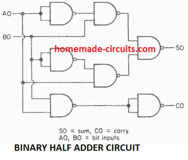
This circuit employs seven NAND gates to create a half adder circuit. A0, B0 constitute the binary digit inputs. S0, C0 represent the sum and carry lines. To be able to learn how these types of circuits function imagine how basic math is educated to kids. You can refer to the half adder TRUTH Table below.
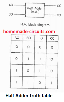
- 0 and 0 is 0
- I and 0 is I sum 1 carry 0.
- 0 and 1 is I sum 1 carry 0.
- I and I is 10 sum 0 carry 1.
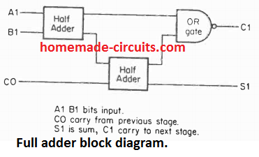
1 0 shouldn't be mistaken as "ten" rather it is pronounced as "one zero" and symbolizes 1 x 2^1 + (0 x 2^0). Two whole half adder circuits in addition to an "OR" gate gives rise to a full adder circuit.
In the following diagram A1 and B1 are the binary digits, C0 is the carry from the previous stage, S1 becomes the sum, C1 is the carry to the next stage.
29) NOR GATE HALF ADDER
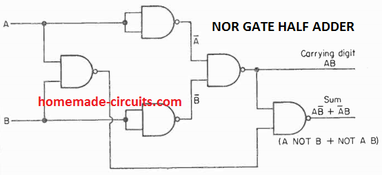
This circuit and next ones below are configured using only NOR gates. The 7402 IC comes with four 2-input NOR gates.
The half adder operates with the help of five NOR gates as depicted above.
Output lines:

30) NOR GATE FULL ADDER
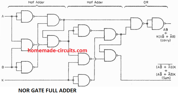
This design depicts a full adder circuit using a pair of NOR gate half-adders along with a couple of extra NOR gates. The circuit works with a total of 12 NOR gates and needs in all 3nos of 7402 I.C.s. The output lines are:

Input lines A, B and K.
K is actually the digit that carries forward from the previous line. Observe that the output is implemented by means of a couple of NOR gates that are equal to a single OR gate. The circuit settles back to two half adders in addition to an OR gate. We can compare this with our previously discussed circuits.
31) SIMPLE SIGNAL INJECTOR
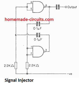
A basic signal injector which can be used for testing audio equipment faults or other frequency related issues, could be created employing two NAND gates. The unit uses 4.5V volt through 3nos of 1.5V AAA cells in series (see diagram 42).
Another signal injector circuit can be built as shown below using a half 7413 IC. This is more reliable since it employs a Schmitt trigger as a multivibrator
32) SIMPLE AMPLIFIER
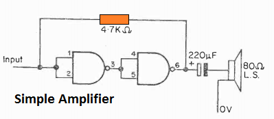
A pair of NAND gates designed as inverters could be wired in series for developing a simple audio amplifier. The 4k7 resistor is employed to generate a negative feedback in the circuit, although this does not help to eliminate all the distortions.
The amplifier output can be used with any loudspeaker rated at 25 to 80 ohms. An 8 Ohm loudspeaker can be tried although that could cause the IC to get a lot warmer.
Lower values for the 4k7 could be also tried but that can lead to lower volume at the output.
33) LOW SPEED CLOCK
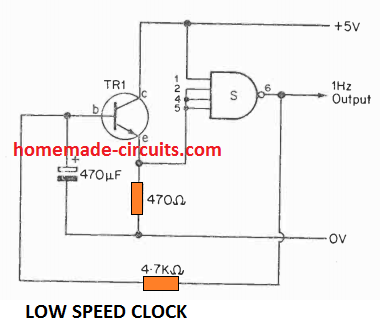
Here a Schmitt trigger is used in conjunction with a low frequency oscillator, the RC values determine the frequency of the circuit. The clock frequency is about 1 Hz or 1 pulse per second.
34) NAND Gate Touch Switch Circuit
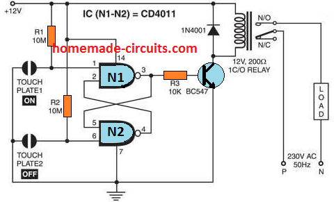
Just a couple of NAND can be used for making a touch operated relay control switch as shown above. The basic configuration is the same as the RS flip flip explained previously, which triggers its output in response to the two touch pads at their inputs. Touching the Touch pad 1 causes the output go high activating the relay driver stage, so that the connected load is switched ON.
When the lower touch pad is touched it resets the output turning it back to logic zero. This action switches OFF the relay driver and the load.
35) PWM Control using a single NAND Gate
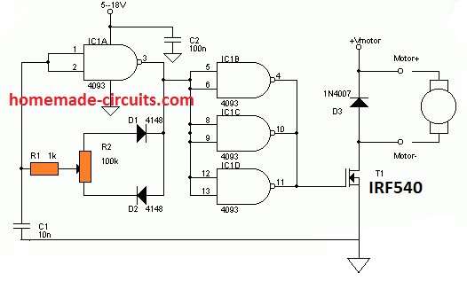
NAND gates can be also used for achieving an efficient PWM controlled output from minimum to maximum.
The NAND gate shown at the left side does two things, it generates the required frequency, and also allows the user to change the ON time and the OFF time of the frequency pulses separately via two diodes which control the charge and discharge timing of the capacitor C1.
The diodes isolate the two parameters and enables the charging and the discharging control of C1 separately via the pot adjustments.
This in turn allows the output PWM to be controlled discretely through the pot adjustments. This set up could be used for controlling DC motor speed accurately with minimum components.
Voltage Doubler using NAND Gates
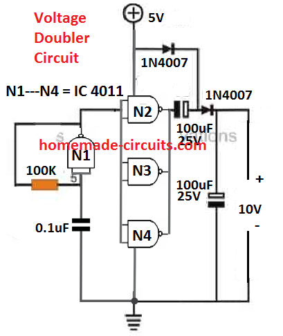
NAND gates can be also applied for making efficient voltage doubler circuits as shown above. Nand N1 is configured as a clock generator or frequency generator. The frequency is reinforced and buffered through the remaining 3 Nand gates wired in parallel.
The output is then fed to a diode capacitor voltage doubler or multipliers stage to finally accomplish the 2X voltage level change at the output. Here 5V is doubled to 10V, however other voltage level up to 15V maximum and be also used for getting the required voltage multiplication.
220V Inverter using NAND Gates
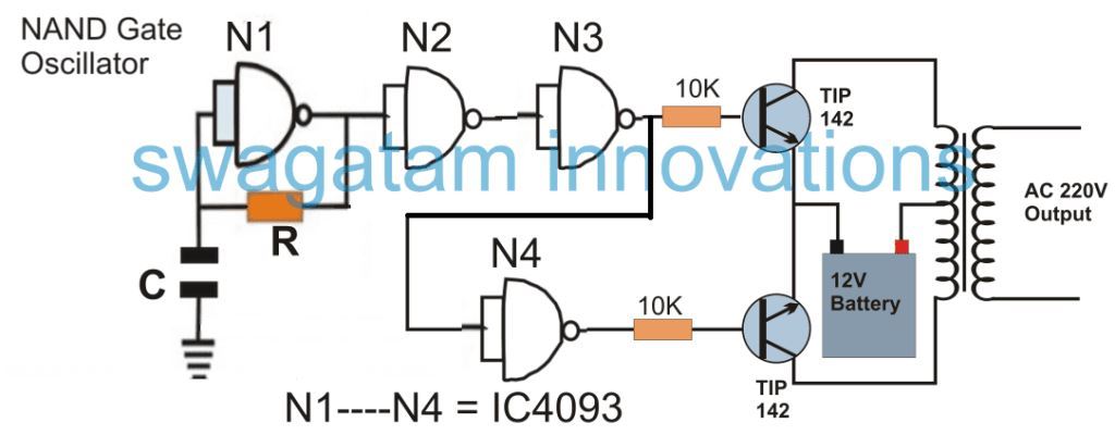
If you are thinking NAND gate can be only used for making low voltage circuits, you may be wrong. A single 4011 IC can be quickly applied for making a powerful 12V to 220V inverter as shown above.
N1 gate along with RC elements form the basic 50 Hz oscillator. The RC parts must be selected appropriately to get the intended 50 Hz or 60 Hz frequency.
N2 to N4 are arranged as buffers and inverters so that the final output at the bases of the transistors produce alternately switching current for the required push pull action on the transformer via the transistor collectors.
Piezo Buzzer
Since NAND gates can be configured as efficient oscillators, the related applications are vast. One of these is the piezo buzzer, which can be built using a single 4011 IC.
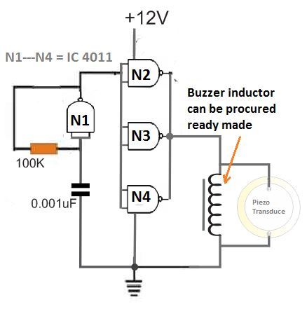
NAND gate oscillators can be customized for implementing many different circuit ideas. This post is not yet completed, and will be updated with more NAND gate based designs as time permits. If you have something interesting related to NAND gate circuits, please let us know your feedback will be greatly appreciated.
Help required to do science project on logic gates. Please share some online link where will get all components. Thanks you in advance
I normally do not buy electronic parts from online shops, instead I go the main market to buy the spare parts so I cannot recommend a specific online shop. I think all the reputed ones are good.
Okay. Thanks for your quick response. Please guide what all I should buy for all logic gate experiments. A list will help. Thanks again
I would recommend you the projects from the following article. The IC is the main part here, and there are hardly any other parts associated with the circuits. All the resistors are 1/4 watt 5%, capacitors with two black plates are ceramic disc types, and the ones which are with black and white plates are electrolytic types:
https://www.homemade-circuits.com/12-simple-ic-4093-circuits-and-projects-explained/
Excellent. Thank you for taking time and effort put these circuits together at one place.
I particularly appreciate giving the internal transistor circuit (I was looking for it and that is how I got into this wonderful link). A description of how the transistor circuit functions as NAND gate would make your work “complete”. In a quick glimpse, I could not see XOR gate. You could include that also.
Thanks once again.
Thanks very much for your useful suggestions, and Glad you liked the post. I will surely consider your suggestions and update the blog accordingly.
For knowing how to use transistors to build a nand gate, you can refer to this article:
https://www.homemade-circuits.com/how-to-make-logic-gates-using-transistors/
Thank you for sharing your knowledge. I have a bunch of these old 7400 series in my parts bin now I can use them to build some projects.
Sounds great! glad you found the article useful.
Remarkable websites you have built………a lot of effort on your part…………by chance have you ever compiled all the files into one pdf that could be downloaded…………again, very impressive…..
Thanks lot for liking this website, no, I haven’t yet compiled the site as pdf to facilitate downloading, but I appreciate your advice, it’s worth considering.
This site has left me speechless.
Thank you very very very much for sharing with us this important work
????
Thank you so much for liking this site!
Grate a lot of information, Im looking for a RF adapter to the meter if You have same around
Thanks friend, presently I do not have this circuit, but I’ll try to find it and let you know, if it’s possible.
Wonderful friend !
Explained and fulfilled.
Nice effort…
Greetings…
Thanks! Glad you liked it!!
Excellent article on using nand gates! Thank you for sharing. I never knew there were so many uses for them.
Thanks for your feedback, appreciate it!