

In this article I have explained 7 easy to build DC to DC voltage doubler circuits using a single IC 4049 and IC 555 along with a few other passive components.
If you are wondering how a simple IC 555 can be used for making a powerful voltage doubler circuit, then this article will help you to understand the details and construct the design at home.
What's a Voltage Doubler
In a voltage doubler circuit an oscillator circuit feeds a high frequency voltage into a specially arranged resistor capacitor network which results in an output DC that is two times higher than the input supply DC.
If you are new to voltage doubler concept and desire to learn the concept in-depth, we have a good elaborate article in this website explaining different voltage multiplier circuits for your reference.
Voltage multiplier concept was first discovered and used practically by British and Irish physicists John Douglas Cockcroft and Ernest Thomas Sinton Walton, hence it is also called the Cockcroft–Walton (CW) generator.
A good example of a voltage multiplier design can be studied through this article which exploits the concept for generating ionized air for purifying air in homes.
A voltage doubler circuit is also a form of voltage multiplier where the diode/capacitor stage is restricted to a couple of stages only, so that the output is allowed to produce a voltage that may be twice of the supply voltage.
Since all voltage multiplier circuits mandatorily require an AC input or a pulsating input, an oscillator circuit becomes essential for accomplishing the results.
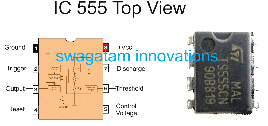
IC 555 Pinout Details

1) Circuit Diagram of a Simple Voltage Doubler using IC 555

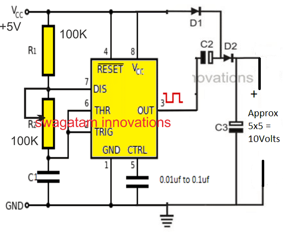
Referring to the above example, we can see an IC 555 circuit configured as an astable multivibrator stage, which is actually a form of oscillator, and is designed to produce a pulsating DC (ON/OFF) at its output pin#3.
If you recall, we had discussed an LED torch circuit in this website, which quite identically uses a voltage doubler circuit, albeit the oscillator section is created using an IC 4049 gates.
Basically, you can replace the IC 555 stage with any other oscillator circuit and still get the voltage doubling effect.
However using IC 555 has a slight benefit since this IC is able to generate more current than any other IC based oscillator circuit without using any external current amplifier stage.
How the Voltage Doubler Stage Operates
As can be seen in the above diagram, the actual voltage multiplication is implemented by the D1, D2, C2, C3 stage, which are configured as a half-bridge 2-stage voltage multiplier network.
Simulating this stage in response to the IC 555's pin#3 situation can be a little difficult, and I am still struggling to get it running in my brain correctly.
As per my mind simulation, the working of the mentioned voltage doubler stage can be explained as given in the following points:
- When the IC output pin#3 is in its low logic or ground level, D1 is able to charge C2, since it is able to get forward biased through C2 and pin#3's negative potential, also simultaneously C3 is charged via D1, and D2.
- Now, in the next instant as soon as pin#3 becomes at high logic or at the positive supply potential, things get slightly confusing.
- Here C2 is unable to discharge via D1, so we have a supply level output from D1, from C2, and from C3 also.
- Many of the other online sites say that at this point the stored voltage inside C2, and the positive from D1 is supposed to combine with the output of C3 to produce a doubled voltage, however that does not make sense.
- Because, when voltages combine in parallel, the net voltage does not increase. The voltages must combine in series to cause the desired boosting or the doubling effect.
- The only logical explanation that can be derived is, when pin#3 becomes high, C2's negative being at the positive level and its positive end also held at the supply level, it is forced to produce a reverse charge pulse which adds up with the C3 charge, causing a instantaneous potential spike having a peak voltage twice that of the supply level.
If you have a better or technically more correctexplanation, please do feel fre to explain it through your comments.
How much Current?
Pin#3 of the IC is assigned to deliver a maximum of 200mA current, therefore the maximum peak current can be expected to be at this 200mA level, however the peaks will get narrower depending on the C2, C3 values.
Higher value capacitors might enable fuller current transfer across the output, therefore make sure the C2, C3 values are optimally selected, around 100uF/25V will be just enough
A Practical Application
Although a voltage doubler circuit can be useful for many electronic circuit applications, a hobby based application could be to illuminate a high voltage LED from a low voltage source, as shown below:

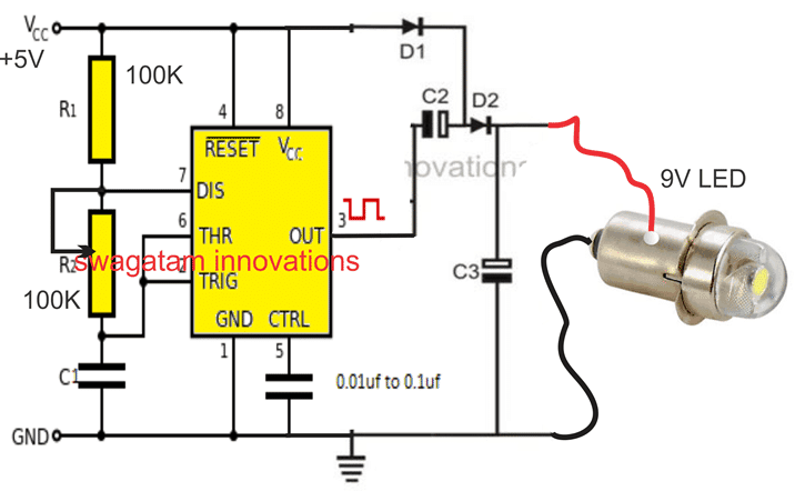
In the above circuit diagram we can see how the circuit is used for illuminating a 9V LED bulb from a 5V supply source, which would normally be impossible if the 5V was directly applied on the LED.
Relation between Frequency, PWM and the Voltage Output Level
The frequency in any voltage doubler circuit is not crucial, however faster frequency will help you to get better results than slower frequencies.
Similarly for the PWM range, the duty cycle should be roughly 50%, narrower pulses will cause lower current at the output, whereas too wide pulses will not allow the relevant capacitors to discharge optimally, again resulting in an ineffective output power.
In the discussed IC 555 astable circuit, the R1 can be anywhere between 10K and 100K, this resistor along with the C1 decides the frequency. C1 consequently can be anywhere between 50nF to 0.5uF.
R2 will fundamentally enable you to control the PWM, therefore this can be made into a variable resistor through a 100K pot.
2) Another 555 Voltage Doubler
The second circuit shown below is another IC 555 based DC voltage-doubler, which produces a DC output voltage that is almost double the supply voltage.

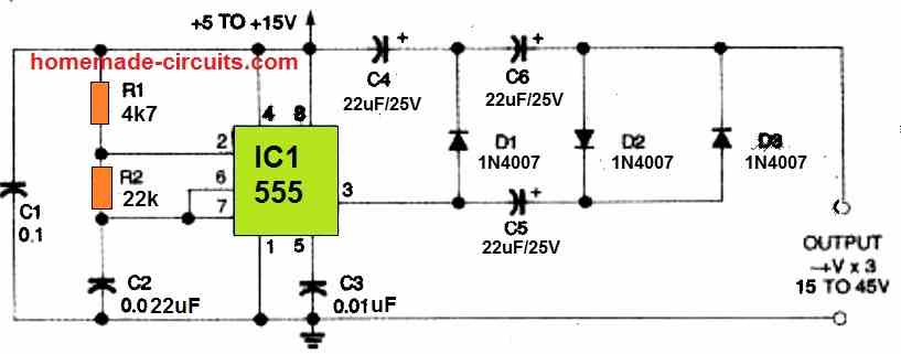
The output of the 555 is connected to a voltage-doubler circuitry consisting of capacitors C4 and C5, as well as diodes D1 and D2.
As long as the output is unloaded, the circuit provides an output that is about nearly twice the supply voltage. The exact value of the output is:
Vout = 2 x Vpeak (Vfd1 + Vfd2)
Where Vpeak represents the squarewave generator's peak output voltage, and Vfd1 and Vfd2 indicate the multiplier diodes D1 and D2's forward voltage drops (approximately 600 millivolts).
As soon as the circuit's output is loaded, the output voltage drops. Any DC source between 5 and 15 volts might operate with the voltage doubler circuit shown above.
This can give voltage outputs across a range of roughly 10 to 30 volts due to its voltage doubling effect. Applying additional multiplier stages to the circuit will result in a higher voltage.
3) Voltage Doubler Using IC 4049 NOT gates
The following CMOS IC based circuit can be used for doubling any DC source voltage (up to 15 V DC).
The presented design will double any voltage between 4 to 15 V DC and will be able to operate loads at current not more then 30 mA.
As can be seen in the diagram, this DC voltage doubler circuit employs just a single IC 4049 for achieving the proposed result.
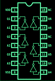
IC 4049 Pinouts

Circuit Operation
The IC 4049 has six gates in all which are all effectively for generating the discussed voltage doubling actions. Two of the gates out of the six are configured as an oscillator.
The extreme left of the diagram shows the oscillator section.
The 100 K resistor and the 0.01 capacitor form the basic frequency determining components.
A frequency is imperatively required if a voltage stepping actions needs to be implemented, therefore here too the involvement of an oscillator becomes necessary.
These oscillation become useful for initialing the charging and discharging a set of capacitors at the output which amounts to the multiplying of the voltage across the set of capacitors in a such a way that the result becomes twice the applied supply voltage.
However the voltage from the oscillator cannot be preferably applied directly to the capacitors, rather its done through a group of gates of the IC arranged in a parallel way.
These parallel gates together produce a good buffering to the applied frequency from the generator gates so that the resultant frequency is stronger with respect to current and does not falter with relatively higher loads at the outputs.
But still keeping the specifications of a CMOS IC in mind the output current handling capacity cannot be expected to be larger than 40 mA.
Higher loads than this will result in the deterioration of the voltage level toward the supply level.
The output capacitor values can be increased to 100uF for getting reasonably higher efficiency levels from the circuit.
With 12 volts as the supply input to the IC, an output of around 22 volts may be acquired from this IC 4049 based voltage doubler circuit.

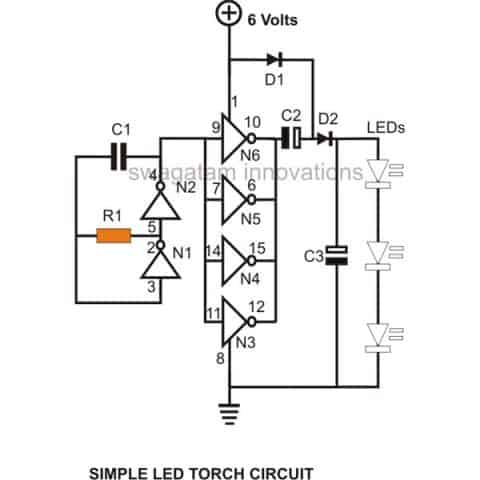
Parts List
- R1 = 68K,
- C1 = 680pF,
- C2, C3 = 100 uF/ 25V,
- D1, D2 =1N4148,
- N1, N2, N3, N4 = IC 4049,
- LEDs White = 3 nos.
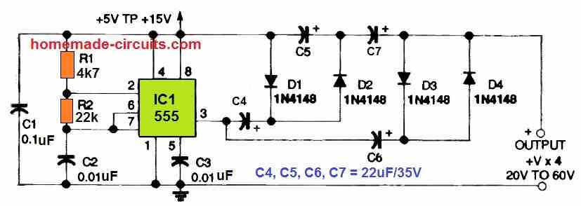
4) Voltage Tripler Circuit
The DC voltage quadrupler circuit shown in the next Figure, can be used to generate output voltages ranging from 20 to 60 volts.

5) Negative Voltage Doubler Circuit
The 5th circuit layout for a DC negative-voltage generator is shown in the following figure, which may produce an output voltage that is about similar in amplitude (double), but with a negative polarity.

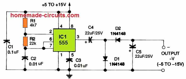
It likewise runs at 3 Hz and powers an output stage that includes capacitors C4 and C5, as well as diodes D1 and D2. The dual output of this circuit can be used to power ICs that need both positive and negative power from a single polarity supply.
6) IC 555 Voltage Doubler Circuit with High Current Output
This sixth high current voltage doubler circuit presents a practical approach to generating a 24 V output from a 12 V battery. It utilizes the 555 timer in astable mode to generate a square wave signal at approximately 1 kHz. Here's how it works:

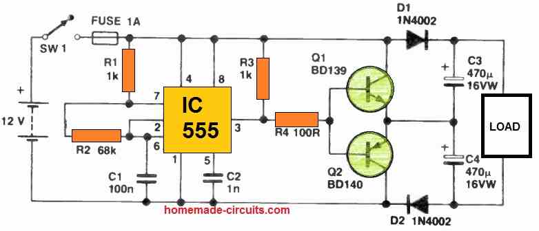
- The 555 timer is configured such that when pin 3 goes high, transistor Q1 becomes conductive, allowing the charging of capacitor C4 to nearly 12 V. Diode D1 prevents the discharge of capacitor C3 during this phase.
- Conversely, when pin 3 goes low, transistor Q2 conducts, enabling the charging of capacitor C3 in a similar manner, while diode D2 prevents the discharge of capacitor C4.
- The combined voltage across capacitors C3 and C4 results in the desired 24 V output.
Under no-load conditions, the output voltage measures approximately 24 V, but it decreases to about 20 V when a load drawing high current of 500 mA is connected.
It's important to note that heat sinks should be applied to the transistors to manage any heat generated during operation due to high current.
The current can be further increased by replacing the transistors with TIP122 and TIP127.
7) 12V to 24V Voltage Doubler Circuit using IC 4093

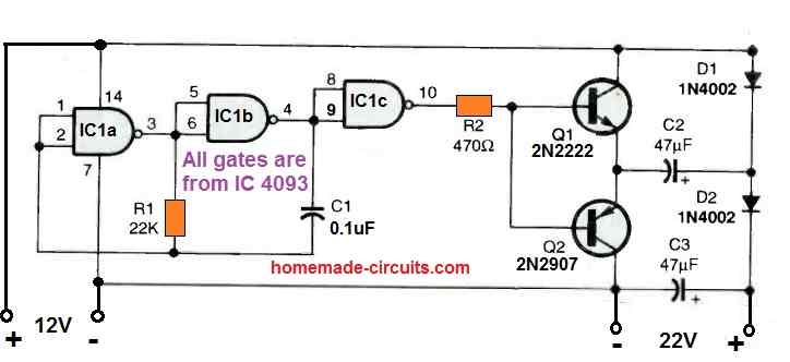
This 7th practical small circuit has an output current capability of 10 to 20 mA and may boost your working voltage by up to 175%.
A squarewave oscillator circuit has been configured using the gates IC1a and IC1b of a CD4093 dual-input NAND Schmitt-trigger CMOS IC.
The gate IC1c is rigged as a buffer for the output. The buffered output from IC1 powers Q1 and Q2 complementary transistors.
The voltage-doubler circuit, which is made up of D1, D2, C2, and C3, is driven by the square wave output at the transistor emitters to provide a boosted output.
The boost circuit will produce 24 volts at around 10 mA with a 12 volt supply, and roughly 18.5 volts at about 20 mA.
Make sure to connect the inputs of the spare unused gate to the ground line of the circuit.