The following article discusses the use of a mosfet as a switch for toggling high current loads efficiently. The circuit can be also transformed into a delay OFF circuit with simple modifications. The design was requested by Mr.Roderel Masibay.
Comparing Mosfet with BJT
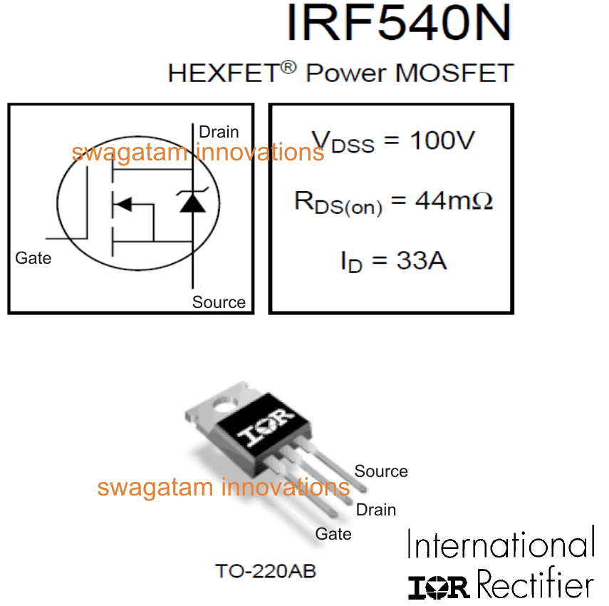
A field effect transistor or mosfet can be compared with a bjt or the ordinary transistors, except one significant difference.
A mosfet is a voltage dependent device unlike BJTs which are current dependent devices, meaning a mosfet would switch ON fully in response to a voltage above 5V at virtually zero current across its gate and source, whereas an ordinary transistor would ask for relatively higher current for switching ON.
Moreover this current requirement grows higher proportionately as the connected load current increases across its collector. Mosfets on the other hand would switch any specified load irrespective of gate current level which may be maintained at the lowest possible levels.
Why Mosfet is Better BJT
Another good thing about mosfet switching is they conduct fully offering very low resistance across the current path to the load.
Additionally a mosfet wouldn't require a resistor for gate triggering and may be switched directly with the available supply voltage provided it's not far too beyond the 12V mark
All these properties associated with mosfets makes it a clear winner when compared to BJTs, especially when it's used like a switch for operating powerful loads such as high current incandescent lamps, halogen lamps, motors, solenoids etc.
As requested here we'll see how a mosfet may be used as a switch for toggling a car wiper system. A car wiper motor consumes considerable amount of current and is usually switched through a buffer stage such as relays, SSRs etc. However relays can be prone to wear and tear while SSRs can be too costly.
Using Mosfet as a Switch
A simpler option can be in the form of a mosfet switch, I have explained the circuit details of the same.
As shown in the given circuit diagram the mosfet forms the main controlling device with practically no complications around it.
A switch at its gate which can be used for switching ON the mosfet and a resistor for keeping the mosfet gate to a negative logic when the switch is in the OFF position.
Pressing the switch provides the mosfet with the required gate voltage relative to its source which is at zero potential.
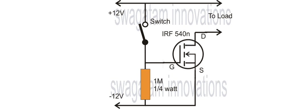
The trigger instantly switches ON the mosfet so that the load connected at its drain arm becomes fully ON and operative.
With a wiper device attached to this point would make it wipe for so long the switched remains depressed.
A wiper system sometimes requires a delay feature for enabling a few minutes of wiping action before stopping.
With a small modification, the above circuit can be simply turned into a delay OFF circuit.
Using Mosfet as a Delay Timer
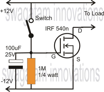
As shown in the diagram below, a capacitor is added just after the switch and across the 1M resistor.
When the switch is momentarily turned ON, the load switches ON and also the capacitor charges up and stores the charge in it.
Video Demonstration
When the switch is toggled OFF, the load continues to receive the power since the stored voltage in the capacitor sustains the gate voltage and keeps it switched ON.
However the capacitor gradually discharges via the 1M resistor and when the voltage drop below 3V, the mosfet is no longer able to hold, and the complete system switches OFF.
The delay period depends on the value of the capacitor and the resistor values, increasing any one of them or both increases the delay period proportionately.
Calculating the Delay
To calculate the delay produced by the RC constant we can use the following formula:
V = V0 x e(-t/RC)
- V is threshold Voltage at which the mosfet is supposed to just switch OFF or just begin turning ON.
- V0 is the supply voltage or the Vcc
- R is the discharge resistance (Ω) which is connected parallel to the capacitor.
- C (Capacitor Value (F) in the exemple 100uF)
- t (time of discharging that we want to calculate (s) )
we want to know the delay (t) = e(-t/RC) = V/V0
-t/RC = Ln(V/V0)
t = -Ln(V/V0) x R x C
Example Solution
If we select the threshold capacitance turn ON/OFF value of the mosfet as 2.1V, and supply voltage as 12V, resistance as 100K, and capacitor as 100uF the delay after which the mosfet will turn OFF could be approximately calculated by solving the equation as given below:
t = -Ln (2.1/12) x 100000 x 0.0001
t = 17.42 s
Thus from the results we find that the delay will be around 17 seconds
Making a Long Duration Timer
A relatively long duration timer may be designed using the above explained mosfet concept for switching heavier loads.
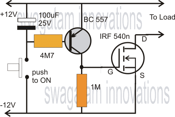
The following diagram depicts the procedures of implementing it.
The inclusion of a extra PNP transistor and a few other passive components enables the circuit to produce higher duration of delay period. The timings may be suitably adjusted by varying the capacitor and resistor connected across the base of the transistor.
MOSFET and SCR Timer Circuit
The MOSFET/SCR timer features a constant-current source to charge C1. C1 and P1 adapt the time range.You are able to adjust C1 throughout a range of 100 and 1000 uF to modify the time period range. Using a 1 ampere relay you are able to control AC loads as much as 100 watts hooked up to the 1 17 VAC or 220 V mains AC.
To use the device, wire the appliance to the relay contacts (points A and B, utilized like a switch) and alter P1 to the preferred time delay. Press S2 do discharge C1 entirely . Then switch ON S1 to begin. Soon after the set time delay has lapsed, the relay will change state, causing the load to switch ON.
On the other hand, if you have selected NC contact of the relay you are able to switch OFF the connected appliance after the set delay is over. To reuse the unit you have to press S2 to discharge C1 prior to starting.
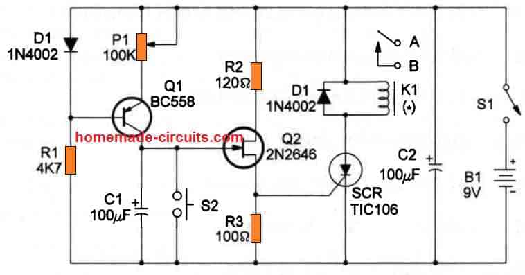
The diagram above shows basic MOSFET timer circuit.
How it Works
When power is switched ON C1 grounds the FET gate, keeping it switched OFF. Q1 acts like a constant current source, and begins slowly charging C1 at a steady constant current rate. The rate of charging of C1 is determined by the resistance of the pot P1. As soon as C1 charges to the Vgs(th) value of the FET, the FET turns ON, and switches ON the SCR, relay and the load.
The time taken by the C1 to reach the Vgs(th) value of the FET is determined by its own value and the resistance of the adjusted pot P1.
