Among the different existing inverter topologies, the full bridge or the H-bridge inverter topology is considered to be the most efficient and effective. Configuring a full bridge topology could involve too many criticality, however with the advent of full bridge driver ICs these have now become one of the simplest inverters one can build.
What's a Full-Bridge Topology
A full bridge inverter also called an H-bridge inverter, is the most efficient inverter topology which work two wire transformers for delivering the required push-pull oscillating current into the primary. This avoids the use of a 3-wire center tapped transformer which are not very efficient due to their twice the amount of primary winding than a 2-wire transformer
This feature allows the use of smaller transformers and get more power outputs at the same time.Today due to the easy availability of full bridge driver ICs things have become utterly simple and making a full bridge inverter circuit at home has become a kids play.
Here I have explained a full bridge inverter circuit using the full bridge driver IC IRS2453(1)D from International Rectifiers.
The mentioned chip is an outstanding full bridge driver IC as it single handedly takes care of all the major criticality involved with H-bridge topologies through its advanced in-built circuitry.
The assembler simply needs to connect a few handful of components externally for achieving a full fledged, working H-bridge inverter.
The simplicity of the design is evident from the diagram shown below:
Circuit Operation

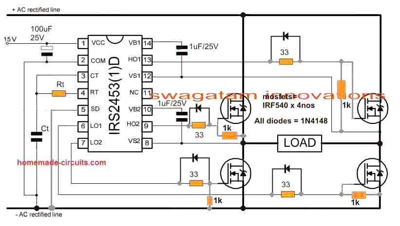
NOTE: Please join the SD pin of the IC with the ground line, if it is not used for the shut down operation.
Pin14 and pin10 are the high side floating supply voltage pinouts of the IC. The 1uF capacitors effectively keep these crucial pinouts a shade higher than the drain voltages of the corresponding mosfets ensuring that the mosfet source potential stays lower than the gate potential for the required conduction of the mosfets.
The gate resistors suppress drain/source surge possibility by preventing sudden conduction of the mosfets.
The diodes across the gate resistors are introduced for quick discharging of the internal gate/drain capacitors during their non-conduction periods for ensuring optimal response from the devices.
The IC IRS2453(1)D is also featured with an in-built oscillator, meaning no external oscillator stage would be required with this chip.
Just a couple of external passive components take care of the frequency for driving the inverter.
Rt and Ct can be calculated for getting the intending 50Hz or 60 Hz frequency outputs over the mosfets.
Important Calculations
Frequency Calculation for IRS2453 Oscillator
The IRS2453 chip uses external components Rt and Ct to set the PWM frequency.
Formula:
f = 1 / (1.453 × Rt × Ct)
- Where:
- f = Switching frequency (Hz)
- Rt = Timing resistor (ohms)
- Ct = Timing capacitor (farads)
Example Calculation:
Let us Assume Rt = 33 kΩ = 33 × 10³ Ω, Ct = 1 µF = 1 × 10⁻⁶ F:
f = 1 / (1.453 × (33 × 10³) × (1 × 10⁻⁶))
f = 1 / (1.453 × 33 × 10⁻³)
f ≈ 20.9 kHz
Thus the switching frequency is approximately 20.9 kHz. So you can adjust Rt and Ct to modify the frequency as needed.
Gate Resistors
The 33ohm resistors at the MOSFET gates limit the inrush current during switching and dampen oscillations.
Power Dissipation in Gate Resistors:
Pgate = Qg × Vgate × f
- Where:
- Qg = Gate charge of the MOSFET (63 nC for IRF540)
- Vgate = Gate drive voltage (10V)
- f = Switching frequency (20.9 kHz)
Substituting values:
Pgate = 63 × 10⁻⁹ × 10 × 20.9 × 10³
Pgate ≈ 0.013 W
Each gate resistor dissipates approximately 13 mW, which is negligible.
Power MOSFET Ratings (IRF540)
Drain-Source Voltage (VDS):
The MOSFETs must withstand the full rectified supply voltage. For a 15V input, VDS(max) must be higher than 15V. The IRF540 has a VDS(max) of 100V, which is adequate.
Current Handling (ID):
Each MOSFET handles half the load current:
ID = Iload / 2
Ensure ID(max) (33A for IRF540) exceeds this value.
Reverse Gate Diodes
The 1N4148 diodes ensures instant gate capacitance discharge for the MOSFETs, which ensures efficient switching response from the MOSFETs.
Reverse Recovery Time:
The recovery time for 1N4148 is 4ns, suitable for high-frequency switching.
Power Dissipation:
Pdiode = Vf × Iload
Where Vf = Forward voltage of the diode (0.7V for 1N4148).
Load Power
The load determines the current through the MOSFETs and resistors.
Load Current (Iload):
Iload = Pload / Vsupply
For Pload = 50 W and Vsupply = 15V:
Iload = 50 / 15 = 3.33 A
Power Dissipation in MOSFETs:
PMOSFET = ID² × RDS(on)
For IRF540, RDS(on) = 0.044 Ω:
PMOSFET = (3.33 / 2)² × 0.044 = 0.122 W per MOSFET.
Capacitor Selection
Input Capacitor (100 µF/25V):
Filters the rectified AC and smooths the supply voltage. The ripple current rating should exceed the load current (Iload).
Bootstrap Capacitors (1 µF/25V):
These provide gate drive voltage for the high-side MOSFETs. Ensure the value can handle the gate charge (Qg) of the MOSFETs.
High Voltage Feature
Another interesting feature of this IC is its ability to handle very high voltages upto 600V making it perfectly applicable for transformeless inverters or compact ferrite inverter circuits.
As can be seen in the given diagram, if an externally accessible 330V DC is applied across the "+/- AC rectified lines", the configuration instantly becomes a transformerless inverter wherein any intended load can be connected directly across the points marked as "load".
Alternatively if an ordinary step-down transformer is used, the primary winding can be connected across the points marked as "load". In this case the "+AC rectified line" can be joined with pin#1 of the IC and terminated commonly to the battery (+) of the inverter.
If a battery higher than 15V is used, the "+AC rectified line" should be connected directly with the battery positive while pin#1 should be applied with a stepped down regulated 12V from the battery source using IC 7812.
Although the below shown design looks too easy to construct, the layout requires some strict guidelines to be followed, you may refer to the post for ensuring correct protection measures for proposed simple full bridge inverter circuit.
Simple H-Bridge or Full Bridge Inverter using two Half-Bridge IC IR2110
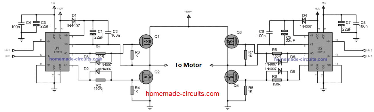
The diagram above shows how to implement an effective full bridge square wave inverter design using a couple of half bridge ICs IR2110.
The ICs are full fledged half bridge drivers equipped with the required bootstrapping capacitor network for driving the high side mosfets, and a dead-time feature to ensure 100% safety for the mosfet conduction.
The ICs work by alternately switching the Q1/Q2 and Q3/Q4 mosfets in tandem, such that at any occasion when Q1 is ON, Q2 and Q3 are completely switched OF and vice versa.
The IC is able to create the above precise switching in response to the timed signals at their HIN and LIN inputs.
These four inputs needs to be triggered to ensure that at any instant HIN1 and LIN2 are switched ON simultaneously while HIN2 and LIN1 are switched OFF, and vice versa. This is done at twice the rate of the inverter output frequency. Meaning if the inverter output is required to be 50Hz, the HIN/LIN inputs should be oscillated at 100Hz rate and so on.
Oscillator Circuit
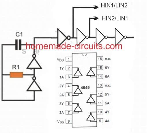
This is an oscillator circuit which is optimized for triggering the HIN/LIN inputs of the above explained full-bridge inverter circuit.
A single 4049 IC is used for generating the required frequency and also for isolating the alternating input feeds for the inverter ICs.
C1 and R1 determine the frequency required for oscillating the half bridge devices and could be calculated using the following formula:
f = 1 /1.2RC
Alternatively, the values could be achieved through some trial and error.
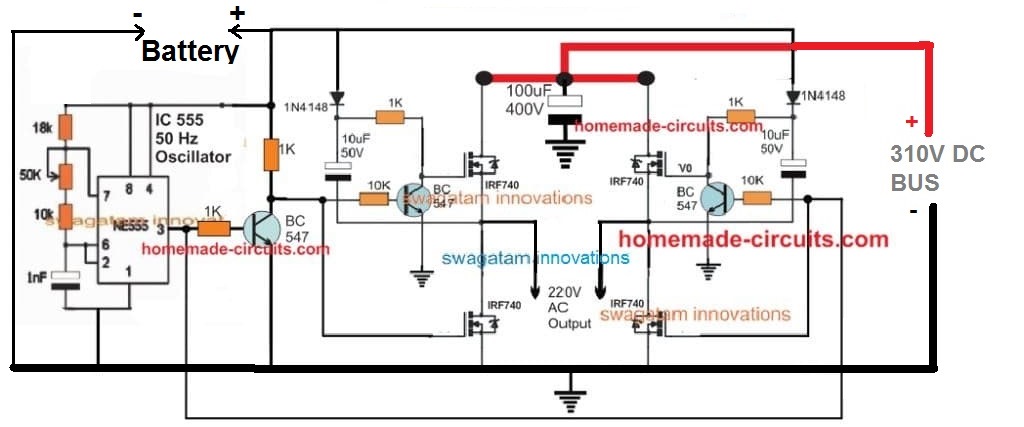
Discrete Full Bridge Inverter using Transistor
So far we have studied a full bridge inverter topologies using specialized ICs, however the same could be built using discrete parts such transistors and capacitors, and without depending on ICs.
A simple diagram can be seen below:
Hi Swagatam,
Congrats! Your web page is cool.
I am looking for good recomendation concerning 1000 VA converter 230V/50Hz to 110V/50Hz.
Do you think using IRS2453 could be good idea?
I have the EG002 (EG8010) in my mind.What would be your idea?
Thank you in advance.
Andy
Hi Andrzej, I think the EG002 can be an easier option, but I can’t figure out how this can be used to convert 220V to 110V? If you use PWM then the average voltage will reduce to 110V but the peak will still remain 220V. A transformer is perhaps the ideal option for converting 220V to 110V.
Hi Swagatam,
Thank you so much for your prompt answer. Regarding PWM you are absolutely right.
I am looking for the solution without transformer – step down converter.
Can you suggest one?
Output voltage could be distorted, no need of ideal sinus.
I appreciate your support very much.
Hi Andrzej,
For 220V the peak voltage is 310V and for 110V it should be around 160V
But without a transformer the peak will remain 310V for 110V sinewave, which is not good. I have no idea how this can reduced to 160V without a transformer?
So I think without a transformer reducing the peak to 160 V may not be possible, or maybe I do not know how to do it.
Hi Swagatam,
Thank you very much for the clarification.
Best regards
Andrzej
I have installed a global inverter circuit using discrete transistors. When I test with 12VDC supply from battery the circuit works fine. Output 11.8VDC, frequency 50Hz. However, when I increase the supply voltage to 42 VDC from behind the diode bridge of an iron core transformer. Then immediately a BC546 (high side) was short-circuited. The corresponding mosfet is also shorted. Can you give advice on this case. Thank you very much.
I think it is due to high voltage spikes which may be destroying the transistors. Try installing 100 V or 150 V rated transistors and see if that helps or not.
Thank you for your quick response chings. Can I replace it with the corresponding type ?
I used Mosfet IRF740, transistor BC547.
Yes, you can replace them with other variants rated at 100V or above.
Bonjour Monsieur,
I am trying to design a full bridge using two IR2153 (instead of IR2110 in your schématics).
I want it to be driven by a single Hall effect IC to replace the RC resonator of your suggested oscillator circuit which triggers the IR21xx ICs.
The purpose is when the Hall IC is High, current in the load will flow one way and when low, the other way.
Any idea ?
Thanks
Hello Lhopiteau,
The IR2153 has a built in oscillator, so it cannot be driven by an external signal from a hall effect sensor.
Hello sir
I’m Jose a freshman in electronic engineering.
I have a project at home which I basically want to achieve inversion of 230vdc 60 amps 50hz to 230vac 60 amps 50hz pure sinewave.
I therefore inquire if I can use a thyristor or how can I go making such inverter with which components specifically?
Hello Jose,
Unfortunately a thyristor cannot be used for switching a DC supply. You will have to implement one of the full bridge designs explained in the above article.
You can first try the basic square wave full bridge inverter as explained above, if you succeed with it then we can proceed with the sine wave integration.
Hello sir,
I’ve followed and built the second schematic which uses IC 555.
I therefore request if I can apply the 235VDC 60 amps on the input labeled battery or should I not exceed a certain Voltage limit?
You should strictly apply only 12V across the points labeled as battery, otherwise the IC 555 will burn.
Hello sir,
I’ve just implemented the other H-bridge with 555IC but I’m yet to connect a power source.
So,my question is should I apply at the input labeled battery the 230VDC 60amps or should be a smaller voltage than the 230VDC?
Thank you sir.
Hello Jose,
I think you should first try it with a lower DC voltage, maybe a 12V or 24V, and if it works only then go for the 220V DC.
good work, what is that some wave inverter all about
Hello, excuse me
I am a final year student and I have to finish this project I am sending you the schematic of the circuit and please guide me what kind of MOSFET to use so that the circuit works well and is not expensive.
Also HIN-LIN waveforms
What do you think I should remove or add in the schematic?
Any help, I thank you
sorry for english
https://freeimage.host/i/gUtZE7
https://freeimage.host/i/grbGDb
From the diagram it seems you are trying to use a transformer as the load across the H-bridge circuit. The connections look OK to me.
I hope the mosfets and the transformer winding ratings are in accordance with the VDD supply
Hello
I measured the gate input voltage of the MOSFETs and it was about 4.3 volts.
Can this low voltage cause MOSFETs to heat up?
To increase the amplitude of my PWM pulses.
have you any recommendation
Yes 4.3V will normally heat up a mosfet since most mosfets are rated to work with a minimum of 9V gate voltage.
However your readings might be wrong, because the output of an H-bridge IC can be in a form of a high frequency, which may not allow you to measure the gate voltage correctly.
PWM amplitude is not related to the output voltage of the H bridge, the Vcc voltage is related to the output voltage from the H bridge. The Vcc should be ideally around 12 to 15V. The PWM peak voltage should not be higher than the Vcc voltage.
In your case as I mentioned earlier, a 900V mosfet can never be used with 4500V supply.
If we use a voltage boosting transformer, should we still use MOSFETs with a voltage of 6000 volts?
According to the design, the primary voltage is about 300 volts, which is converted to 4500 volts in the secondary.
According to the above information, is it correct to choose 2SK3878, ID=9A, VDSS=900V MOSFET?
If you are using the 4500 V across the drain/source of the mosfets then the mosfets will need to be rated at over 5000 V or 6000 V. If you are using 300 V across drain/source of the mosfets then your existing 900 V mosfet will be OK.
Thank you for your response
This internal dead time (IR 2113) is enabled, or needs to be enabled.
In which part of the datasheet is it referred to?
Unfortunately it is not mentioned in the datasheet but it is an understood fact that dead time will be existing in the IC by default. If suppose the IC does not provide a dead time internally then the IC will simply not work and it will keep blowing the mosfets which I don’t think the manufacturers of the IC will allow to happen.
This IC is popularly used for making inverters and in no circuit diagram an external dead time has been seen so far.
The main thing is that the mosfets must be rated much higher than the load supply specifications. If the mosfet rating is less than the input supply then it will keep blowing.
No, the output voltage is completely DC and the output ground is connected to the MOSFET ground with a 22 nanofarad capacitor
If the mosfet supply is DC then it is fine, but make sure mosfet VDSS rating is higher than the supply voltage used.
For MOSFETs, I used 2sk3878 with 900V voltage and 9A current.
In this circuit, the output voltage is 4500 volts with a current of 0.005 amperes
900 V can never handle 4500 V supply. The MOSFETs must be rated at least at 6000 V. Meaning the VDSS should be equal to 6000 V minimum.
Yes, the output voltage is DC
This is the circuit diagram for creating dead time.
which is designed for a delay time of 1 microsecond
https://freeimage.host/i/UteuFp
Do you think it is well designed?
The IR 2113 already has a dead time built-in, so there’s no need to create an external dead time.
Thanks for your tips
I create a voltage of 4500 volts using a step-up isolation transformer.
The primary voltage of the two ends is around 300 volts, which the transformer converts to 4500 volts.
How can I send you the map?
If you have used the second diagram from the above article then I can understand the design, no need to send the diagram. However if you want to show the diagram, you can upload it to any “free image hosting site online” and provide the link to me here.
I guess you have used 4500V DC across the drain and the ground of the mosfets. Please Remember the 4500V must be a DC, not AC, otherwise the mosfets will burn.
In that case you will have to upgrade all the mosfets and the capacitors to high voltage rating as suggested in my previous comment.
Thank you for asking this question.
Are you sure the output is 4500 voltage?
Which mosfets did you use? For 4500V output the mosfets must be rated at minimum 5000 to 6000V
Hello
Thank you in advance for sharing your experience.
I am building an H bridge.
80 kHz switching frequency.
The output voltage is 4500 volts.
The driver used is IR 2113.
Designed for a dead time of 1 microsecond.
Problem:
When I test the driver without connecting to the MOSFETs, everything is correct and there is no problem.
But when I connect HIN1/LIN2 MOSFETs Q1 and Q4 and HIN2/LIN1 to MOSFETs Q2 and Q3 and connect the drain voltage, one of the MOSFETs and two IC drivers burn.
Please help me
At 4500V the risks can be very high.
You will have use mosfets that are rated at 6000 V, and the bootstrapping capacitor must be rated at 10000 V. You must have reverse diodes rated at 10kv across mosfet drain/source.
The Vcc pin of the IC must be protected with a 1K series resistor, a filter capacitor, and a 12V zener diode.
The mosfets must be connected as close as possible to the IC. The +/- 4500V DC bus line must have a non polar capacitor rated at 10uF / 10000 V.
Also remember that the HIN and LIN polarities must be perfectly opposite while switching. Meaning when HIN is high, LIN should be LOW and vice versa.
Another thing is that, if you are two IR2113 ICs, the HIN pin of one IC should be connected with the LIN pin of the other IC, so that the mosfest are able to switch diagonally.
The second question is where the last two Gates NOT are connected in the 4049 circuit
Those two gates are extra gates in the IC, they are not used. Just connect them as they are shown in the diagram.
Hello Boss, I built the IRS2453 circuit and it worked but where I have issues is, when I connect 1k across the gate/source of each MOSFET, the output voltage is around 144v instead of 220v but when I remove the resistors, it gives me 220v. Transformer is 12v/220v. Pls what could be reason for this?
That’s great Patrick,
1K should have been fine, I am not sure why you are facing this issue. You can try replacing the 1K with 4k7 or 10K resistors and see how it works.
Thanks for your quick response. I have used 10k yet i can’t get 220v. With the resistors at the gate/source pin, I realised about 4v on the load(where the transformer is expected). Don’t know if the 1uf used for bootstrapping should be made higher, perhaps that might solve the issues.
In that case I think you can eliminate the gate/source resistor for the high side mosfets. However keeping it connected on the low side mosfets won’t have any problems.
Thanks Boss, I’ll try this one and give you a feedback soonest. I sincerely appreciate your good contributions.
Sure thing! Let me know if you have any further questions.
dear Swagatam;
I was able to bridge h with help from this site. thanks but i’m trying to make my circuit better. I want to add IR2110. My circuit is running at 20khz. What are your thoughts? frequency generator ir2153 or (sg3525) hin1 and hin2 connections should be. and your thoughts.
Thank you Mesut, I am glad you could build the H bridge circuit.
you can use the frequency generator circuit which is shown in the 3rd diagram using 4049. Using SG3525 or IR2153 can be quite complex.
in the picture inspect (mosfet gate R5 and R7) does it act as a voltage divider? then mosfet gate (10.4348volt) then R5=47ohm R7=10kohm mosfet gate (11.94volt) wouldn’t the mosfet gate be nicer? Can I use D5,D6,D2,D3 ST4148 diode? and what is the meaning of this diode?
I finished this circuit with IR2153 and IR2111 and I am making my final preparations to try it. I have to calculate the resistance values well, I don’t have much luck if I burn it.
sorry for english.
The gate/source resistors are to increase working efficiency of the mosfets, so that their gate capacitance discharges as quickly as possible during OFF times and the mosfet generates less heat. The diodes also do the same thing, discharges the gate capacitance of the mosfets quickly during OFF times
yes you can use 1N4148 diodes.
Full bridge to drive DC motor ,DIS,about dead time,then pwm1,pwm2,to drive,one way,or back,direction,what,s happen and circuitry how to drive by logic signals?,, ,,,no answer
Hello, thank you for your scientific help. Please help me by using irs2453 and ir2110 for induction furnace circuit. Thank you.
Hi, you can perhaps try the following concept:
https://www.homemade-circuits.com/induction-heater-circuit-using-igbt/
Sayın SWAGATAM.Transistor ve 555’entegreyle yapılan H köprü inverteri yaptım fakat devre çalışmıyor sorun nerede? düzeltip bildirir misiniz? Teşekkür ederim
Hello Sezgin, without checking your circuit practically, it can be difficult to understand the fault.
I am waiting your working circuit schematics please
All the above circuits are tested and verified designs. They have been tested by many of the readers.
Can i also use two of this dual IGBT?
FF150R12RT4
IGBTs can be replaced for MOSFETs, but I am not sure about the specific number you have mentioned.
Thank you very much sir ????
My pleasure!
Hello sir, according to the final circuit do I need to use resistors to discharge the gate capacity?
Hello Buddhi, resistors are not required, gate capacitance is discharged by the BC547 transistors
Me encantan esos proyectos me gustaría hacerle una consulta espero vea mi comentario
hi, can I use this method for product frequency above 1MHz?
I need help troubleshooting the half bridge inverter using a IR2110. Can you help me out?
Hi, I would like to use a 4049 to make a oscillator and use a IR2110 to make a half bridge for creating a wire power transfer circuit. However, I just have one rectifier, and cannot fully apply your circuit. How can I modify your circuit above, so I can make my circuit work? Thank you!!
Hi, you can use a single diode rectified voltage, by including a high value filter capacitor across the rectified lines. The capacitor could e in the order of 500uF/400V
Sir,
Mosfets connected to pins 13 and 8 do not switch ON at all. accordingly no output power.
do you have any comments.
Thanks
Please check the frequency across the Ct capacitor, if you get a frequency there, then your IC is oscillating and the MOSFET may be faulty, if no frequency then your IC is faulty or some other part/connections are faulty…
Any oscilloscope can quickly indicate the working of the IC.
Sir,
RE:Simple full bridge inverter using driver IRS2453dpdf
I just made similar circuit using 20VDC battery with voltage divider (16V power tge driver) but l used mosfet FQP16N25 instead of IRF540.
at the end the circuit not producing AC power at all.
l am not sure what is the problem, is it the mosfet type or what.
I appreciate your advise. Thanks
Sam, did you connect the shut down SD pin to ground. Please check out the revised diagram, showing the SD pin connected with ground, and 1k resistors connected across the gate/source of all the MOSFETs
Yes sd pin connected to the ground, also today l connected 1k resistors to the gate of mosfets.
mosfets connected to pins 8 and 13 never switch ON. other two mosfets used to switch ON.
Thank you so much sir. Sir my question is about the first design (IRS2453). Those it means the ic is manufactured with the bootstrap and death time circuitry, or we can still add them to the circuit? Thanks hope to hear from you soon
The bootstrapping is already added in the circuit through the relevant diode and the capacitor, however, the values of these parts may need some variations depending on the frequency specifications of the system…
OK thank you sir like in my case the frequency is 50 to 60HZ and my DC supply is from a 48v serially connected battery instead of the rectified 220v ac than from there my output AC will be fered to the primary of a step up transformer to get my 220v AC. I hope there shouldn’t be any changes with the circuit. Thanks in advance
Yes, no serious changes required, except the bootstrapping capacitors which could be increased a bit until the most optimal MOSFET conduction and power output from the transformer is achieved
Am so greatfull sir but still am confused when you say “the value of the bootstrapping capicitors could be increased” Do you mean the capacitance or voltage rating of the Capacitors?, or are the capacitors non polarized type? Please sir can you kindly propose the capacitor values for me?. And lastly how can I provide a feedback circuit for my 220v stabilization? Thanks so much sir mey the lord be your strength ????.
It is the capacitance that may need to be increased, not the voltage rating. You can refer to the following diagram for the values
https://www.homemade-circuits.com/wp-content/uploads/2019/11/full-bridge.png
Once you complete it successful we can discuss the feedback.
Sir I need a complete guidelines on inverter design from scratch typically pure sine wave inverter using iron steel core transformer
George, You can read the following articles for the required information
Inverter tutorial
convert square to sine
Hi Swagatam, hope you well.
Hope you can help me with an idea i have with this named IC, called IRS2453(1)D.
Firstly, what is the chances to use two Hall effect transistors to do the timing of the IC? with other words, I have a rotor with say 10 small button magnets on, alternating between north and south. Then, using latching Hall effect tr’s which get switched on and off my the north and south magnets. then to use that switching sequence as the CT and RT timing for the said IC.
Secondly, my need is to use 2 of the said IC’s as to control a type of motor with the following working condition. the motor has 4 sets of electro-magnets and sits at the following positions, one at twelve o’clock and six o’clock and then the other two at three o’clock and then obviously at nine o’clock. The 12 o’clock and 6 o’clock works together and then obviously the other 2 works together, but with the distinct difference that at a one moment the 12 o’clock electro-magnet is a north pole and the 6 o’clock is a south pole. Then the next moment the sequence is reversed and the 12 o’clock electro-magnet has a south pole and the 6 o’clock has a north pole. Obviously the other pair works in the same manner due to the full H-bridge sequence and topology.
It has to be understand that when the one set op electro-magnet poles are sw’ed on the other pair has to be off. There has to be a certain on time and off time as to push and pull the magnets on the rotor to be moved. For better understanding of the motor, the rotor has 8 magnets which means at one moment each of the electro-magnets has 2 magnets, one north and one south. Thus when say the 12 o’clock eletro-magnet is sw’d on and forms a north pole, the it will push the north pole magnet on the rother and obviously pulls the south pole magnet. again it will be understood that the opposite electro-magnet will form a south pole and here again the logic is the same by the fact that the south pole magnet on the rotor will be pushed and the north pole magnet will be attracted. It will be then understood that this is the sequence of the other pole pair as well.
Here is where my first question came up as to see if i can use button magnets on a smaller rotor which is spaced accordingly as to sw on and off the hall effect tr’s as to cause the timing of the 2 H-bridge IC’s, causing the correct timing of the IC’s. It must beobvious to you now that i need to have a perfect sequence between the to timing H-bridge IC’s.
In fact Swagatam, this is a simple sequence when one uses a commutator, but its not the technology i want to use, but rather a electronical way and this said IC’s working is so simple that I am sure there must be a simple way to do it. My experience is 2-way radio’s and the repair of it and not in design of circuits as you are experienced in. Thus my reaching out to you and see if you might be able and eager to help as i get the idea when i went threw your web site that you enjoy designing and thinking outside the box.
So my friend, hope this i tried to explain to you is understanding and that it might inspire your to the point of thinking about it and design if necessary to help me in my little project.
Hope to hear from you and have a great day!
Regards
Ben Burger
Thank you Ben, I have understood your requirement, but I am having difficulty figuring out how the 4 sets of magnets can be switched with an H-bridge configuration.
It may be possible using a sequential IC such as a 4017, but not with an H-bridge, according to me.
Hi Swagatam, thank you for replaying…sorry my friend, I tried to explain the motor by saying there is 4 electro magnets where in fact there is 8. The purpose was to make it as plain as possible as to ensure you get the idea i tried to explain by using the analogy of the clock and the position of the electro magnets on the clock. There is in fact 2 electro magnets next to each other with a bit of a gap between them and the next 2 electro magnets. Its then also important to know that with 2 sets of electro magnets….which is directly opposing each other, there is 3 magnets for each set of electro magnets, which interact with the said electro magnets. It must be understood that when this two sets of electro magnets are active, on eletro magnet has a north pole and the adjacent electro magnet is then a south pole. At this specific moment of operation, with the one electro magnet a south and the adjacent eletro magnet a north, it causes the 3 permanent magnets to be pushed and pulled. It should be obvious that the operation of the opposite set of active electromagnets works exactly the same at the given moment. At this precise moment, the other two sets of electromagnets which is inactive, has each 2 permanent magnets right across it. With the rotor which is turning a few degrees the inactive electro magnets gets turned on and thus push the PM away as well, adding to the torque.
I hope I made the operation a bit more understandable.
I have considered the option of using a sequencer but came across this H-bridge IC and was wondering if it might work better.
I don’t want to put the motor diagram on this forum but if you like, as to understand this motor’s operation i will send you a sketch of it to your personal email address.
hope to hear again from you.
Friendly regards
Ben
Thank you Ben, I have already understood your explanation, and therefore I said 4 sets of electromagnets which corresponds to 8 electromagnets, where each pair is connected opposite to one another.
H bridge cannot be used here, because H-bridge can be triggered only through 2 complementary pulses, for operating a single flip-flop load.
If you are having other alternatives for operating this set up, then you can surely try them, because a Full bridge or an H bridge does not appear to be feasible for this application.
Hi Swagatam, thank you for your replay and have a great day.
Regards
Ben
You are welcome Ben….
hello sir I need to make 24V dc to 220 AC 2kw inverter without using transformer can you please help me to chose the circuit diagram for that
Hello Amin, you can try the concept explained in the following article:
https://www.homemade-circuits.com/5kva-ferrite-core-inverter-circuit/
But it is meany only for those who have reasonably good experience and knowledge in the field of SMPS dsigns
For what you need this ? make from 24 vdc to 240 ac you need transformer.
Hi can i ask you in circuit with IC IRS 2453 D can I use H-bridge SKM400GB124D Semikron IGBT Module 1200v 400A ? instead irf 540 . I just need 200 A for aluminium welding.
Hi, yes you can use it.
Many thanks
Can i ask you : In aluminium welder there is foot pedal for restriction current when welding aluminium.
This current restriction is for regulation put down current when material is heating up.
How i can restrict, put down current in this circuit ?
Thanks, You can do it by adding a current limiting resistor in series with the ground line between the ICpin2 or Ct ground point and the MOSFET ground point. And then connect the SD pin with the MOSFET ground point.
The value of the resistor will decide when the IC shut down is activated for limiting the current
thanks
Dear sir, I am making a 1000 watt 24 volt Inverter using the above full wave bridge circuit. I am confused regarding which Transformer to use? Can I use a single tap 24 volt transformer rated at 30 amps? I will be using 2 x 12 volt 150AH Batteries in series to make 24 volts.
Firdosh, yes you can use a 0-24V/30 amp/220V transformer but 30 amp will give 1000 watts, you will need minimum 50 amp
Is the circuit with the Ir2110 mosfet driver suitable for making a 100 watt solar panel inverter?
The power output depends on the MOSFET rating, so you can get any desired power output simply by upgrading the MOSFETs accordingly. 100 watt can be achieved using IRF540 or any similar mosfets
Brother, is there any N channel mosfet and P channel mosfet pair that has Vds of >400V and how do I know how much resistance of resistor should I put to the gate of mosfet if I ever replace the 4 mosfet in the first circuit diagram which uses IRS2453D and what to do to increase the power of it? Thank u very much in advance.
Hi Martin, you can use any 400V P channel mosfets but add 4 in parallel on each channel
For N channel you can use any standard 400V N mosfet and use single MOSFEts on each channel.
For the gate resistance you can use 220 ohms
Brother, what is the maximum power of the first circuit diagram which uses the IC IRS2453D and four IRF540 mosfet? Thanks in advance.
It can handle up to 300 watts
Como vai? Tem um esquema mais simples, para mandar sinal HIM LIM em um ir 2110 / Obrigado.
It is given using IC 4049…it is a simple design to drive HIN, LIN
Again sir, please help me understand the meaning of “SD being used for shutdown” is the shutdown same as switching off the inverter,how then can this be achieved? Please help with a diagram is possible.
Shut down will shut off the output of the IC, which will switch OFF the MOSfets completely.
Hello sir swagatam,how is this achieved is it by the use of a scr? If so can you help with a diagram showing the connection?
Evans, you can connect the SCR cathode to SD pin, anode to `12V supply, and gate to the input signal through a 1K resistor
After the ic output is shut down through the SD pin ,how is the system reset back again?
the outputs restores cutting off the feedback and the inverter begins working again.
Please go through the pinouts functions here
https://www.homemade-circuits.com/understanding-sg3525-ic-pin-outs/
Sir swagatam,how can I advance the circuit to produce a pure sine wave with pwm, kindly help me with a circuit diagram if at all it’s possible to integrate pwm to the system,thanks.
Evans, for this you will have to integrate the SPWM to the low side MOSFFET gates, it is not difficult, but making the basic full bridge design could be difficult
Sir from the above circuit irs2453(1)D,if was to integrate spwm with opamp,which pins of irs2453 will give me low and high pulses that I should feed to the opam (-)&(+) inputs?
You will have to do it in this way
THe slow triangle to the op amp should come from the CT pin of the IC, and fast triangle can be from any other source such as IC 555 etc
Wooow,sir u can’t imagine how of help you’ve been,thank you very much and May the Almighty God bless you. Sir can mosfets be added in parallel for higher currents? How can this be done,is there any changes to the circuit? Or is just connection of drains, sources and gates together? How will the gates be driven?
Thank you Evans, you can connect more MOSFETs in parallel without any changes in the circuit. Gates will be driven in parallel.
hello sir swagatam,please how can i maintain the stability of the output irregardless of the loads or no loads at all?
help with a circuit diagram and the connection to this irs2453 circuit
https://www.homemade-circuits.com/wp-content/uploads/2020/01/sine-full-bridge.png
Evans, you can do it using the following circuit
https://www.homemade-circuits.com/wp-content/uploads/2014/01/inverter-output-voltage-corrector-circuit-1.png
You can remove the diodes from the transistor collector and the connect the collector directly with the Ct pin of the IC.
Hi sir,i constructed this Inverter and it’s working fine. I was thinking of converting it to an inverter charger using ;
1. Same transformer
2. Mosfets body diodes
Again another concern is how to boost the charging voltage because I used a 0-14v transformer and I need to charge my 2 × 12v 200Ah batteries fully.
Please sir help me with step by step circuitry so that I can implement this thanks.
Hi Evans, I will have to research the concept, if it’s feasible I’ll try to post it soon. For boosting you will have to employ a boost charger, as suggested previously.
Hello sir swagatam, suggest for me any spwm that you have ever posted that is compatible with this ic irs2453(1)D that won’t give me a hard time integrating since I don’t have any scoop to view the wave pattern.
without scope it can be very difficult and may result in failures….
How is the setting of the 10k preset?
Again instead of using the inverter output directly,is it advisable to use a separate power supply say a feedback transformer?
finally i thank you for your quick,unconditional responses
https://www.homemade-circuits.com/wp-content/uploads/2014/01/inverter-output-voltage-corrector-circuit-1.png
Feed 220V on the left side (220k side), adjust the preset until the transistor just activates. That’s all.
You can replace the 3 V zener with an LED to get the direct indication of the cut off activation when the inverter output goes beyond 220 V
very well noted sir,thank you very much
Glad to help!
Very well noted sir
Evans, it actually seems quite easy, since the external diodes are in a bridge formation, we simply need to cut off the gates of the MOSFETs from the oscillator IC through a DPDT relay, when AC mains is available at the grid output, Simultaneously, transformer secondary side will also need to be switched to the the grid AC side via another DPDT relay. By default the MOSFET gates must be connected to their sources via a 1k resistor.
I will try to update the info through a new article soon.
Thank you sir for the response,if I could ask, should I cut off the oscillator from the gates or cut off the supply to the oscillator or cut off both?.
Evans, cutting of power to the oscillator IC should be a better option, which can done with a single SPDT relay. But make sure to keep a 1k resistor permanently connected across all the MOSFET gate source pins.
Hello sir swagatam,how about the irs2453(1)D circuit diagram full bridge? Is it difficult to build full bridge using the chip? Again sir ,is there any need for a bjt stage for this chip design? If so how to go about it?
Evans, if you do everything correctly then the chances of any damage to the MOSFETs can be less. You will have to experiment with the 1uF capacitor, which could be anywhere between 4.7uF to 22uF. While doing this make sure to connect a appropriate bulbs in series with the drains of the MOSFETs, the bulbs must not illuminate without a LOAD attached, this will confirm the inverter is working OK.
Ok sir, what’s the formula for calculating the values of CT and rt?
sir swagatam,can a 20v transformer charge a 24v battery? also sir help me know how calculate the current of a transformer at no load? coz i have a transformer with an output of 20v,input is 240v but it has no indication of the current. But te secondary site the coil gauge used i can see awg6. help please ill appreciate.
Hi Evans, yes it can after adding a bridge rectifier. After rectification the output from the bridge will be 20 x 1.41 = 28.2 V.
To know current output you can connect a 20 amp ammeter in the AC range directly across the secondary wires for a couple of seconds, and check the reading.
oooh,thank you sir swagatam. now one more question
what if the current is more than 20?
cause the transformer is very huge like 30kgs,wont it destroy the ammeter?
The meter range must be approximately 2 times more than the anticipated current from the source.
Hello Sir
This circuit looks very interesting. I am working on making such an inverter circuit but with a three phase output from a DC input. May you please assist me with a circuit diagram and code if it has to include some coding.
My last question is how do you compare the suitability of microcontroller based designs and the IC above if the intended application is converting DC from solar to three phase AC
Hello Morgan, you can try one of these designs:
https://www.homemade-circuits.com/arduino-3-phase-inverter-circuit-with-code/
Arduino is absolutely not necessary for making any inverter, to me it’s an overkill unless there’s some specific reason behind it.
Good evening Swagatam,
Your discrete h bridge inverter circuit without the ic, how many wattage is it? Pls can you design a 5kva discrete h bridge inverter without the ic?
Hello Freedom, it will depend on which MOSFETs you use in it, the ID and the VDSS of the MOSfeT will decide the max wattage.
sir i want to use IR2153 with inbuilt programmable oscillator having formula for f = 1/(1.4 x (Rt + 75ohm) x Ct. if i calculate the switching frequency of oscillator using its low & high pulse for mosfet driving as 50Hz. will it not be the same as the output frequency provided to the load?
Sheraz, the high pulses across Ct switches the high side and the low side outputs of the IC sequentially, therefore for completing each cycle (high + low switching) at the output, the Ct frequency will need to be 100 Hz, as per my understanding.
dear sir! what will be the switching frequency of the mosfets or IGBTs produce by ic IR2453 for 50Hz output wave or it is 50Hz determined by calculating Rt & Ct pins of the ic?
Dear Sheraz, according to me it should be 100 Hz across Rt, Ct. 50 Hz should be at the mosfet bridge output
Please sir ur digram is correct but it was not a without center tap project… I am purchase this transformer(without center tap) sir…. Please recommend other sir.. In ur inverter project i show many inverter project in which using ic 555 and without centre tap… Except two batteries project… Can i choose one of them… Sir… And also suggest me which one is…
Apurva, IC 555 or any similar oscillator IC will always require a center tap transformer for an inverter configuration, unless two batteries are used.
Ok sir… I am agree with ur rply but sir can u provide me without ic 555 and without centre tap transformer project. Even it has complex than also i can tryfor make it.. But their parts will common which are found in my place…. I send u one cricuit diagram in ur email id see it and clarify it it best for me or not… And also give me some knowledge about that circuit… Please sir i always believe on u sir… Please help me
Apurva, I did not receive any email from you, please show me the link here!
(wordpress@162.240.8.81) it is ur link… Where u send me a msg…..and i am also send the cricuit digram in this link….
Can you show me the link of the diagram instead? or the link of the article?
This ic not present in my place. Sir
Other two ic whivh have same configuration i search in Google but they also not found in my place sir… Please recommend common full bridge drivers ic aur if other suitable diagram which have using ic 555.. Please send me… Please sir i am very happy if u can do for me… Please sir
Hi Apurva, In that case you will have to use two batteries for making a full bridge inverter using any ordinary IC like 555 or 4047 etc. You can even use the following concept with two batteries for getting a full bridge output
https://www.homemade-circuits.com/2012/09/mini-50-watt-mosfet-inverter-circuit.html
Sir i show in ups box 600va/360w where we can take this transformer…. And i can check it with 2 bulb100w but time will be to not measure… How much will be glow it
If you do it, the battery will get damaged quickly…
7amp x 12=84watt then i can use four 12v 7ah battery then it given 300watt power sir… Battery will connect into parallel connection….
yes that’s possible.
but even then battery will get damaged if it’s used at its full 7Ah level.
Thanks sir… One more question can i use irs2453D instead of any pwm driver… Please recommend me.. Sir
Apurva, this IC is a full bridge driver IC, it is not a PWM driver, it will only provide you a square wave inverter, but an very efficient full bridge inverter
Sorry for writing in to comment… Sir i want know can i use any full bridge drivers ic ir2453 in place of any other ic which have same configuration.. Because it was not found in my area… Please suggest me…which ic used in place of this ic…
Yes you can use any full bridge IC and make the circuit as per its datasheet.
Please rply me sir i am waiting for ur answer… And also tell me can i use ic ir 2153 in place of it…
IR 2153 is a half bridge IC, you will need two of them to make it full bridge.
It contain ac power supply for run this this project… But i want run only battery power supply sir.. And used of without centre tape transformer… Because these item would be purchased… Now
You can run it with battery also. Just connect the pin#1 of the IC with the upper line, and then you can use 12V battery across the upper line and the lower line.
How much watt will generate by centre less tranformer output supply sir.. If i use 600va ups transformer…
It will depend on the battery also. With 7Ah you are gong to get not more than 50 watts for an hour.
Can i glow 2bulb of 100w by this project… Aur not
When I have already said that with 12V 7Ah battery you can operate only 50 watt load, then how can 2 100watt work? Please learn the basics first ans then attempt these complex circuits.
If i want generate 500w from this cricuit… How much amp battery used with this ups transformer… And also clarify me Can this ups transformer oprate 500w output power… When i introduced ur recommended amp battery…
Yes can get 500 watt from a 600va transformer, You will require minimum 200Ah deep-cycle battery for this.
But sir… When this transformer present in ups which are operate by 12v 7ah battery and produce 360watt output how it is possible sir…
did you practically put 360 watt and check? 360 watt will draw 30 amp current… from where will the battery will bring 30 amp? 7Ah can produce maximum 7 amp current, and at this rate it will be flat and destroyed within 30 minutes. Even at full 7 amp the max power will be 7 x 12 = 84 watts