In this post I have explained how to make a simple sine wave inverter using bubba oscillator sine wave generator. The idea ws requested by Mr. Ritwik Naudiyal.
Technical Specifications
I am a 4th year B.Tech Student Electrical Eng.
We are trying to make pure wave sine wave inverter using PWM and bubba oscillator for our Final project, also along with it a battery charging and auto cut off circuit would be needed
We want the inverter to work for day to day purposes. We would be grateful to you if u can give a working circuit fr this.
thank You!
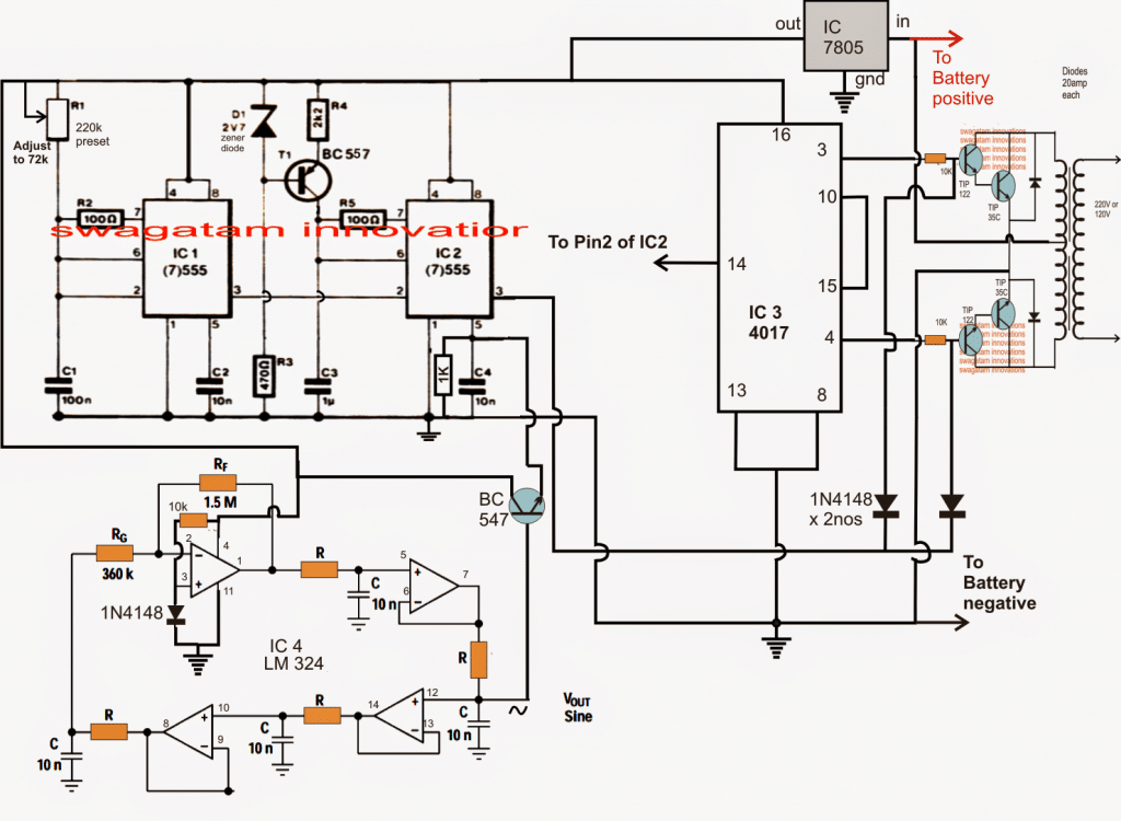
Circuit Diagram

NOTE: Please use a Darlingtton pair for the BC547 connected with pin#5 of IC2 for efficient PWM conversion.
The Design
The proposed sine wave inverter using bubba oscillator may be understood with the help of the following points:
The stage comprising two 555 ICs are configured as PWM generators where IC1 forms a square pulse generator for the PWMs while IC2 forms the monostable PWM generator with respect to the modulation input applied at its pin5.
The sine wave modulation input at pin5 of IC2 is ahieved with the help of a bubba oscillator created by using four opamps from the IC LM324.
The generated sine wave pulses are fixed at precise 50 Hz and fed to pin5 of IC2 via a BJT common collector for further processing.
The 50 Hz Formula
The 50 Hz for the bubba oscillator is set by selecting R precisely with the help of the following formula:
f = 1/2(3.14)RC
IC2 compares the sine wave modulations at its pin5 with the square pulses at its pin2 and generates an equivalent PWM waveform at its pin3.
The flip flop stage reqired for switching the power stage is configured through a single IC 4017 whose outputs are appropriately integarted with the two high gain high current power BJT stage formed by Darlington TIP122 and TIP35.
The pin14 of the 4017 is clocked at around 200 Hz via pin3 of IC1 in order to achieve a 50 HZ switching across the power transistors.
The PWM modulation of the above 50 Hz switching is implemented with the help of the two 1N4148 diodes connected across the bases of the tIP122 and are switched in accordance with the PWM from pin3 of IC1
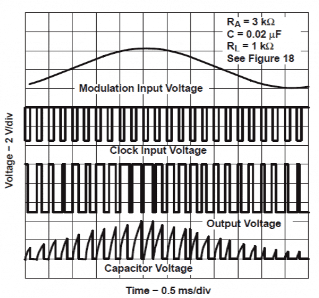
Assumed waveforms of the PWMs may be referred in the following image:
Waveform Bubba Oscillator

